TECHNICAL MANUAL
000 DC 0 000000 00 0000 000 ODD 00 0 oooonnn n-'
1 Z~4S'J"IDI11213141SKll~H~~unMUHU.7
1111111111111111111111111"
2222222222222222222222'
ill-
~cc
L~PI~ PI~~~~PI
3333333333333331 ' "44444' .
5 5 5 5
66F 77
II
I
I I
JANUARY 197.2
DOCUMATION
IMPORTANT NOTICE
THIS TECHNICAL MANUAL IS SUPPLIED
WITH DOCUMATION CARD READER SERIAL
NUMBER
7
30
/,"~,.
THIS MANUAL SHOULD REMAIN WITH THAT
TECHNICAL MANUAL
oooocoooooooooooooooooooooooooonnnn "
I Z J ~ 5 ' ; I 91011I?1JU1SI'111'112I1Z12221Z"2Si'21211~ 1111111111111111111111111' '
2 2 Z 2 1 2 1 2 1 2 11 2 2 1 22 2 12 1 2 • 333333333333333'''' 44444"
5 5 5 5 6 6 F 77 B,
P DOCUMATION. INCORPORATED. 1971
Contents of this manual may not be repro-duced in whole or in part without written
permission of Documation, Incorporated.
II
I
I I
JANUARY 1972
DOCUMATION
I
I N C O R P O R A T E D POST OFFICE BOX 1240Technical Manual Change Record
This Technical Manual has been updated to reflect Customer Specifications. Minor changes
to text or schematics are marked on the pages affected. Major changes to text or schematics
are corrected by direct replacement of pages affected, or are contained in an Addendum.
Customer:
Model:
Frequency
uo0,-,O _ _ _Options:
Addendums:
Text Changes:
Scliematic Change
Title
Wiring Diagram, AC Power Distribution, 115 VAC,
60Hz ••••••••
Wiring Diagram, AC Power Distribution,
230VAC,
50Hz ••••••••
Card Cage, P. C. Card Location , •••••••••••••••••••••••••
Wiring Dia.gra:i:n, Card Cage ••••••••••••.
-' •.•••••••••••••
Wiring Diagram, Control Panel • • • • • • • • • • • • • • • • • • • • • • . • ••
5V Power Supply, 115 VAC,
60Hz . . . .
5V Power Supply, 230 VAC,
50Hz . . . .
Solenoid Driver, 115 VA C,
60Hz •••••••••••••••••••••••••
Solenoid Driver,
230VA C,
50Hz •••••••••••••••••••••••••
Clock Card A"ssembly . . . •
Schematic, (sheet 1 of 3) •••••••••••••••••••••.•••••••
Schematic, (sheet 2 of 3) •••••.••••••••••••••••••••••
Schematic, (sheet 3 of 3) •••••••••.••••••••••••••••••
Error Ca.rd Assembly . . . ,
Schematic, (sheet 1 of 2) ••••••••••••••••••••••••••••
Schematic, (sheet 2 of 2) ••••••••••••••••••••••••••••
Sync Card Assembly . . . • .
1 . . . .Schematic, (sheet 1 of 3) ••••••••••••••••••••••••••••
Schematic, (sheet 2 of 3) ••••••••••••••••••••••••••••
Schematic, (sheet 3 of 3) ••••••••.••••.••••••••••••••
Control Card Assembly ••••••••••••.•••••••••••••••••••
Schematic, (sheet 1 of 2) •••••••••••••
' •••••••••••••••
Schematic, (sheet 2 of 2) ••••••••••••••••••••••••••••
SpecialCa.rds:
• e· II! • . • .. • •
Doc. No.
--+!t~2~o.:;;...oO",",-,O,--
_ _
Verified
TABLE OF CONTENTS Introduction General Specifications Operation General
Initial Setup
Loading the Input Hopper
Unloading Stacker
Switches and Indicators Rear Panel Switches
Operational Flow Chart
Theory of Operation Card Track
Data Recovery
Oscillator/Four-Phase Clock Logic
Pick Control Logic
Sync Control Logic
Preset Counter Logic
Offset Count/Storage Register Comparator Logic
Wide-Strobe Control Logic
Character Buffer/Output Logic
Column Counter Control Logic Control Logic
Motion Check Logic
Lamp Drivers
Interface
General
Timing Connectors
Signal Characteristics Grounding
i
Page No.
TABLE OF CONTENTS Continued
Preventive Maintenance
General
Cleaning
Lubrication
Repair
General
Repair Procedures Table of Contents
Required Tools
Replacement of Hopper Empty Switch
Adjustment of Picker Sector Travel
Adjustment of Tension on Main Drive Motor Belt Adjustment of Stacker Tray Spring
Stacker Shaft Support-Bearing Replacement
Replacement of Belt on Vacuum Pump Motor Assembly Replacement of Main Drive Motor Belt
Replacement and Adjustment of Magnetic Pickup
Replacement of Solenoid
Reolacement of Roller Bearings, Read Head or Light Station
To Replace Roller Assembly Bearings
To Reolace Read Head
To Replace Light Station Replacement of Picker
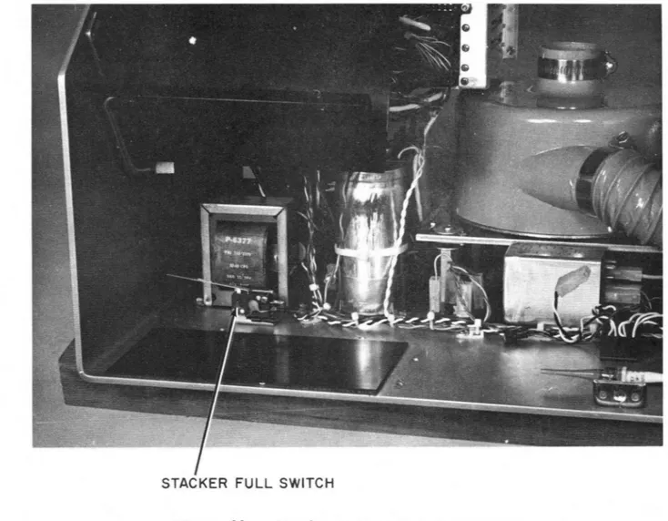
Reolacement of Stacker Full Switch Replacement of Stacker Photocell
Electrical Drawings
Parts List
Signal Mnemonics and Abbreviations
Page No.
36
36 36
38
39
39 39
39
41 41 41 44 44
46
49
52 52
55
57
58
58
60
61
61
Appendix A
Appendix B
Figure No. 1 2 3 4 5 6 7 8 9 9 10 11 12 13 14 15 16 17 18 19 20 21 22 23 24 25 26 27 28 29 30 31 32 33
LIST OF ILLUSTRATIONS
Three-Quarter Front View Three-Quarter Rear View Switch Location
Operational Flow Chart
M Series Card Reader Logic Block Diagram Timing Relationship for Standard Punched Card Oscillator/Four-Phase Clock Logic Block Diagram Pick Control Logic Block Diagram
Sync Control Logic Block and Timing Diagram (Sheet 1 of 2)
Sync Control Logic Block and Timing Diagram (Sheet 2 of 2)
Preset Counter Logic Block Diagram Comparator Logic Block Diagram
Wide-Strobe Control Logic Block Diagram Character Buffer Storage Logic Block Diagram Column Counter Control Logic Block Diagram Control Logic Block and Timing Diagram
Standard Interface Timing for M Series Readers Circuit Characteristics
Removal of Fan Screen Solenoid Lubrication
Three~arter Front View Three-Quarter Rear View
Partial Front View, Cover Removed Picker Sector Adjustment
Partial Front View, Stacker Spring Rear View, Cover Removed
Rear View, Cover and Rear Connector Panel Removed Front View, Main Wiring Connections
Front View, Main Mounting Plate Removal Vacuum Pump Belt Adjustment
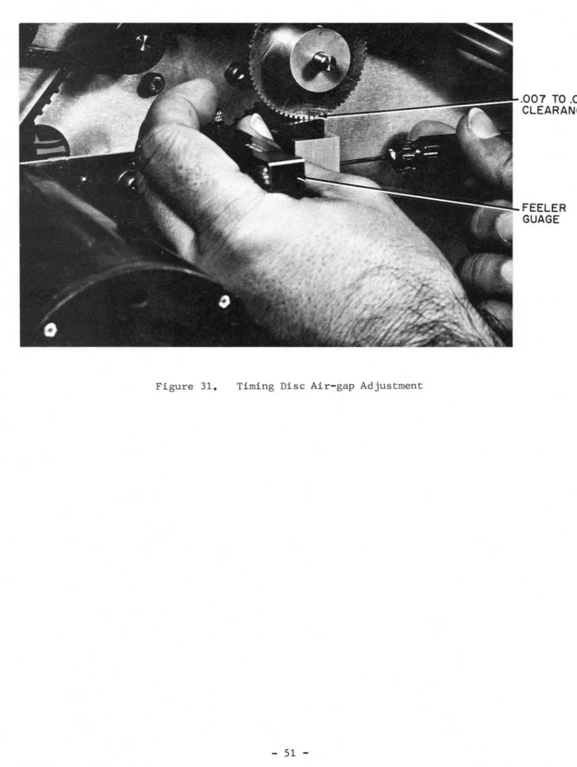
Bottom View, Main Mounting Plate Timing Disc Air-gap Adjustment
Stacker Casting Removal and Bearing Replacement Solenoid Replacement and Adjustment
i i i
Figure No.
34
35
36
37
38
39
LIST OF ILLUSTRATIONS Continued
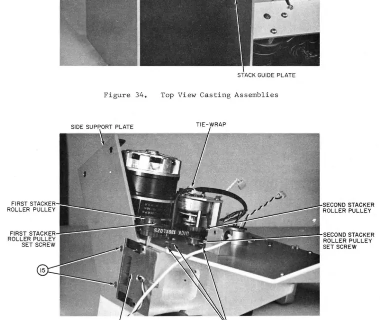
Top View Casting Assemblies
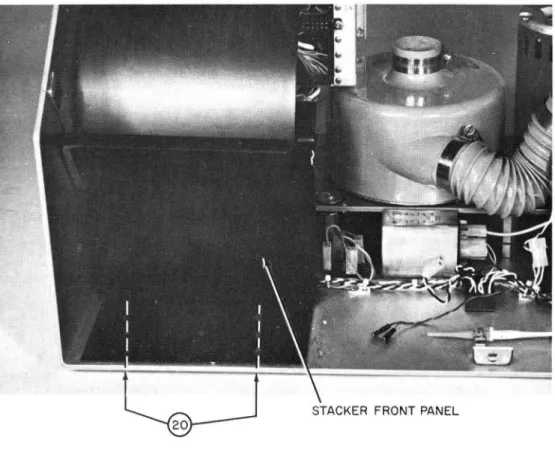
Bottom View Main Drive Motor Assembly Top View Stacker Casting Assembly Stacker Panel Removal
Stacker Full Switch Replacement Main Frame Component Location
Page No.
56
56 59
59
62
INTRODUCTION
GENERAL
This manual provides operational, interface and maintenance information
for the M 200 Punched Card Reader manufactured by Documation Incorporated, 841 East New Haven Avenue, Melbourne, Florida 32901. The manual is
section-alized to cover operational instructions, theory of operation, interface
details, preventive maintenance, and repair. The appendix includes electrical schematics and wiring details.
The M 200 Card Reader shown in figures 1 and 2, is designed to read
standard EIA l2-row, 80 column punched cards. The hopper capacity is
ade-quate to hold approximately 550 cards of .007" thickness. These are sepa-rated from the stack sequentially and moved past a phototransistor read
sta-tion where the data is recognized in a serial, column-by-column manner. The
cards are then stacked into the output hopper in the same order as they were
originally put into the reader. The reading cycle is externally controlled
for single card selection or continuous run. In the continuous mode, the
reader will read 300 cards per minute.
The M Series card readers are specifically designed for continuous duty
operation in adverse operational environments. The chassis is of heavy duty
construction and all components have been chosen to provide for rugged,
relia-ble performance. The vacuum-type picker has a remarkable tolerance to
muti-lated, warped, and edge-damaged cards. The short card track and gentle
accel-eration forces of the card handling mechanism yield insignificant wear so that
card decks routinely last in excess of 1000 passes.
The information contained in this manual is accurate and complete as of the date of publication. Documation will continue to improve both its products
and the effectiveness of its documentation. Comments and suggestions as to
how this manual may be improved are solicited. Address comments to:
Engineering Writer
Documation, Incorporated
Post Office Box 1240
Melbourne, Florida 32901
(305) 724-1111
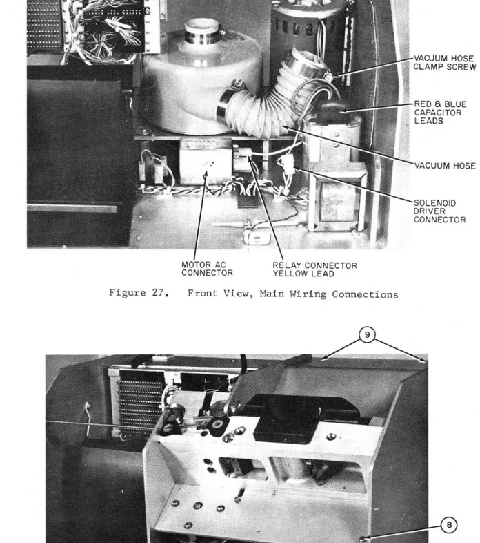
-Figure 1. Three~uarter Front View
Reading Speed:
Card Type:
Control:
Hopper Size:
Stacker Size:
Power Requirements:
Voltage:
Power:
Size:
Height:
Width:
Depth:
Weight:
M 200 SUMMARY SPECIFICATIONS
300 cards per minute maximum in continuous run.
Single Card Cycle: 200 milliseconds.
Standard 80 column EIA card.
Demand feed, one card-at-a-time under external
program control. Reader will continuous run as
long as the Pick Command remains TRUE.
4.0 inches (approximately 550 cards of 7 mill
thickness) •
4.0 inches (approximately 550 cards of 7 mill
thickness) •
115 VAC ±lSV, single phase, @ 60 hz (standard model)
230 VAC ±30V, single phase,
@
50 hz (export model)950 VA starting load for 3 sec
400 VA running load
11 inches 27.9 cm
19\ inches 48.9 cm
14 inches 35.5 cm
60 1 bs • 27.3 kg
-OPERATION
GENERAL
The following paragraphs provide description and instructions for normal
op0ration of the M Series Card Readers. All operator controls and indicators
are described with turn-on/shut-down instructions included. Refer to figure 3
for the location of switches and indicators mentioned in the following
descrip-tion.
INITIAL SET-UP
1. Upon receipt of a new reader from the manufacturer, the two ~ 8-32
screws in the bottom plate must be removed. These lock the blower motor plate for shipment to prevent damage to the motor plate vibration isolators. If the
reader is to be reshipped, these. screws should be retained and reinserted prior
to packing.
2. Plug in the AC power cord. Notice that this is a clockwise twist-lock connector.
3. Set the MODE switch (rear panel) in LOCAL.
4. Set the SHUTDOWN switch (rear panel) in AUTO.
5. Switch the CIRCUIT BREAKER (power switch) to energize the reader
(motors will not come on at this time).
6. Press the LAMP TEST switch and observe that all front panel indicators
illuminate.
7. Load a deck of cards into the input hopper.
8. Press the RESET switch. The motors should come on after a short
delay (approx. 3 seconds) and the cards should be picked and stacked. When the
input hopper is empty, the motors should shutdown and the HOPPER CHECK light
illuminate.
9. This completes the initial off-line operational test.
LOADING THE INPUT HOPPER
Loading the input hopper with punched cards to be r~ad is performed as
follows:
1. Pull the hopper follower back with one hand and load the card deck
into the hopper area; the first card to be read must be placed at the front
with the "9" edge down, column 1 to the left. Continue placing cards into the
EJ
r···
····r··--.---r---
r--.---;
I
~TOPII
RESET~
:
:
:
:1...---1--i READ ~ PICK : STACK ; HOPPER :
j CHECK
!
CHECKi
CHECK 1 CHECK :t~
____________
oj ______________ j ________ . __.1 ____________
1o o
FRONT CONTROL PANEL
AC POWER SWITCH
REAR PANEL
LAMP TEST ~ SHUTDOWN
~ MAN~AUTO
MODE
REMOT<~LOCAL
Figure 3. Switch Location
-CAUTION
DO NOT PACK THE INPUT HO~~ER SO FULL
THAT THE RIFFLE ACTION IS INHIBITED
2. The hopper may be loaded while cards are being read if the operator is
careful to keep tension on the front portion of the deck while loading additional
cards at the rear. This is best done with the input hopper approximately ~ to
1/3 full. Use just enough pressure to maintain the riffle action.
3. Unloading the input hopper is the reverse of the loading procedure. Normally all cards are processed through the reader; however, if it is necessary to unload the hopper, push the follower down and remove the card deck. If the
cards are arranged in a particular order, exercise care in repacking them in
their storage container so that the order is maintained.
UNLOADING STACKER
To unload the stacker, perform the following steps:
1. Pull stacker follower back with one hand and remove the front or rear portion of the card deck from the stacker area, being careful that deck order
is maintained.
2. The stacker may be unloaded while cards are being read.
SWITCHES AND INDICATORS
POWER (toggle circuit breaker and indicator)
All power to the card reader is controlled by this circuit breaker. Since
the indicator is supplied by the +5V power supply, it is illuminated only when
power has been applied to the entire AC distribution system. Toggling the switch (indicator is illuminated) in down position removes the power from the
card reader.
STOP (momentary-action pushbutton/indicator switch)
Actuation of the STOP switch immediately overrides the PICK COMMAND and lowers the READY line. The card reader will stop operation after the card
cur-rently in the track is read completely; power is not removed from the reader
by this action. The red STOP indicator is illuminated as soon as the switch
is depressed.
RESET (momentary-action pushbutton/indicator switch)
Actuation of the RESET switch clears all error flip-flops and initializes
all counters. The reset action is initiated by the return stroke of the RESET
READ CHECK (indicator)
The READ CHECK alarm indicator denotes that the card just read may be
torn on the leading or trailing edges or have punches in the 0 or 81st columns.
The READ CHECK will cause the reader to stop. If it occurs on all cards, it
is an indication of a fault in the read electronics.
STACK CHECK (indicator)
The STACK CHECK alarm indicator denotes that the previous card was not
fully seated in the output hopper. Check the card track to make sure it is clear
and check the stacker for a badly mutilated card.
PICK CHECK (indicator)
The PICK CHECK alarm indicator denotes that a card has failed to reach
the read station after a PICK COMMAND has been received. Inspect the cards in
the input hopper for excessive leading edge damage, torn webs, or cards stapled
together. If so, remove the staple or straighten the card and reinsert.
If no apparent card damage is present, check for excessive card deck
warpage (in excess of 1") and/or ink glaze buildup on the picker face. Clean
the picker face with solvent.
HOPPER CHECK (indicator)
The HOPPER CHECK alarm indicator denotes that either the input hopper is
empty or the stack hopper is full. This is a normal operational occurrence.
REAR PANEL SWITCHES
LAMP TEST (pushbutton switch)
Depressing the LAMP TEST switch illuminates all front-panel indicators to
determine if an indicator lamp is inoperative.
MODE (toggle sWitch)
When placed in the LOCAL position, this switch disables the PICK COMMAND input to the card reader and allows the operator to run the reader off-line by
depressing the RESET pushbutton switch on the front panel. When placed in the
REMOTE position, this switch enables the PICK COMMAND input to the ~ard reader,
which places the reader on-line for normal remote control operation. Data and
other output signals are present at all times.
SHUTDOWN (toggle switch)
When placed in the MANUAL position, this switch energizes the motors for
continuous operation whether or not cards are in the input hopper. When placed in the AUTO position, this switch provides an automatic shutdown of the motors
-when the input hopper is .empty. The motors will automatically restart when
cards are placed in the hopper and the RESET switch is depressed.
delay of approximately 3 seconds for the motors to run up.
Expect a
OPERATIONAL FLOW CHART
Figure 4 shows a flow chart of the sequence of events which may be encountered
in operating the reader. If trouble is experienced, refer to this check list
before calling for maintenance.
SET SWITCHES TO DESIRED MODE
PICK CHECK ALARM IS RAISED
CHECK FIRST CARD IN HOPPER FOR STAPLES OR SEVERE MUTILATION
CH ECK PICK SHOE FOR INK BUILD UP SCRUB WITH ALCOHOL
CHECK FOR PROPER VACUUM ACTION AND RIFFLE AIR
I. CHECK THAT CIRCUIT BREAKER IS ON. 2. CHECK FOR PROPER OPERATING
VOLTAGE AN 0 FREQUENCY.
DEPRESS L.AMP TEST SWITCH TO. ASSURE PROPER
OPERATION ON INDICATORS
HOPPER CHECK ALARM REMAINS ON WITH HOPPER
PROPE RL.Y LOADED
NOTE'
----p(jWER CORD CONNECTED TO PROPER VOLTAGE • FREQUENCY AVAILABLE BEFORE POWER SWITCH IS DEPRESSED.
INSPECT LAST CARD I N STACKER FOR TORN LEADING OR TRAILING EDGE
I NSPECT LAST CARD FOR 'SEVERE DAMAGE OR STACKER BLOCKAGE
HOPPER IS EMPTY OR STACKER IS FULL
THEORY OF OPERATION
CARD TRACK
The Documation card reader line is unique in several respects, in that card wear is insignificant and a card jam is virtually an impossibility. The card track is designed around a patented vacuum picker which works in conjunc-tion with riffle air in the input hopper to produce a card reader which is very tolerant to damaged cards. This tolerance extends to cards which have been badly worn, edge nicked, warped, bent, folded or otherwise damaged as a result of rough handling.
The riffle air acts on the first half inch of cards in the input hopper so that they stand apart, individually "air cushioned" from the rest of the card deck and each other. This prevents the cards from sticking together in case of static electricity, hole locking, or torn webs. Should the cards have been subjected to high humidity conditions prior to being loaded into the card reader, the riffle air also minimizes the effect of swelling or frictional increases between the cards.
The picker mechanism utilizes a strong vacuum to grasp the bottom card,
and upon command, draw i t away from the bottom of the stack. The card is smoothly accelerated through the wide throat into the constant speed drive rollers. The design of the vacuum picker and its associated throat block prevent the unit from double picking so well that cards which are even stapled together will not enter the card track. Should cards which are stapled or taped together be inadvertently put in the input hopper, the card reader will stop, indicating a FICK CHECK. The operator can remove the staples, separate the cards, re-enter them in their proper position in the deck and resume reading.
The card track itself is very short so that at no time is more than one card in motion. The combination of damaged card tolerance, gentle card treat-ment and short card track have produced a card reader which is virtually jam proof. Card life has proven to be in excess of 1000 passes.
DATA RECOVERY
The logic block diagram for the M Series card reader is shown in figure 5. The description that follows applies to all Documation M Series punched card readers since the reliable recovery of data from cards passing down the card track is accomplished in the same manner regardless of track velocity.
-READ 13 STATION ~ ~ STACK
~
STATION CONTROLPANELS 3
7
INDICATOR DRIVERS
HOPPER
SWITCHES 4'
480 KHZ OSCILLATOR
2
4 -I/> CLOCK ,
LOGIC II
READ 12
INTERFACE
,
PICK3
2 CONTROL4
-PCK CONTROL LOGIC ,
6 5'
I I
5'
COLUMN COUNTER
-POR CI
I I
I
1
I
I
I
I
J
I I
I
- -
3{
RESET
--GPR
-'- SYNC
PRESET
:2 CONTROL
COUNTER ZERO
PICKUP
DATA LINES TO EXTERNAL
QUIPMENT
- -
PICK-I PCR
I
I
I 'I
I
I'
12
I
- -
84CRI---5'
SOLENOID DRIVER
SOLENOID
PICK CMD
STATUS LINES
INDEX MARKS
IMST WIDE STROBE CONTROL 3 STCPC
I 2
E
FR OM EXTERNAL EQUIPMENT
}
S
TO EXTERNAL EQUIPMENT
TI/>D
I COMPARATOR
The heart of the card reader electronics is the control logic and sync
control, where the internal logic timing and the movement of the card past the
read station is synchronized to enable accurate sequential interpretation of
the data on the card. Primary logic timing is established by the 480-KHz
crystal oscillator and the associated four-phase clock logic, whose outputs are
used to shift, store, and control other timing operations. Card movement speed
is established by the hysteresis synchronous drive motor, belts and steel drive
rollers. A timing disk consisting of a ferrous notched wheel is mounted on the drive roller shaft. Synchronization input to the logic is derived from the
magnetic reluctance pickup associated with this timing disk. Sufficient
reso-lution is provided such that two signals are produced by the pickup for each card data column as it is moved through the card track at the track speed of
the particular M Series reader being used.
When a PICK COMMAND is received from the external program control, card
processing will be started provided no alarm conditions exist with the card reader powered up. The Pick Control logic then produces a PICK signal to the
Solenoid Driver, a PCLK signal to the control logic, and a pick-command reset
(PCR) to the sync control. These actions initialize the various control
cir-cuits and energize the solenoid to pick a punched card from the input hopper.
If a card does not reach the read station, the PICK CHECK alarm is raised.
The read station and stack station utilize phototransistor sensor arrays
to both read the card hole pattern and to monitor card movement. When a card
is picked and moved into the card track, the leading edge is detected by the
first phototransistor in the read station to go dark. This produces a Good
Pick Reset (GPR). As the card continues to move past the read station, the
various control circuits are synchronized with the card movement to enable
interpretation of the column data contained in the card hole patterns and to output this data at the same timing point for each of the 80 columns.
Since GPR is generated by the leading edge of the card, its occurrence is also utilized to start the synchronization process necessary for the precise
generation of the data column strobes. At GPR, the Preset Counter is enabled
to produce an interval equivalent to the time it takes the card to move 0.049
inches. The value of this preset interval is different for each reader model
and is hard-wired into the counter. Its value establishes the time that should
elapse from the detection of the leading edge of the card to the occurrence of the first possible data column 0' (see figure 6). The first two data holes
-I I
GPR
. 2 S 0 " 4
.223"
1+----+..;.----PRESET COUNTER
INTERVAL
i
I
r-,
r-,
0
1 1 I 1
I I I 1
~J I 1
~-l
o·
0DC
NOTES·
---0
r-,
I I 1 I
L.J
80 81
I 1 DC
(I) DASHED LINES INDICATE PSEUDO HOLES IN CARD. (2) DC = DARK CHECK
LC = LIGHT CHECK GPR = GOOD PICK RESET
(3) HOLE SIZE EXAGGERATED FOR EXPLANATION.
r...,
., r-,
I I I I I 1 I I I I L.J ...J
LJ
82 83 84
are actually pseudo-columns, since by EIA standard, no data appears in the
first 0.223 inches of the card.
When the Preset Counter ZERO signal is produced, indicating the end of the
preset period and the start of card data columns, the Offset Count is set to synchronize the card reader logic to the signals from the magnetic pickup.
This offset is the value of the count accrued during the time from the
begin-ning of pseudo-column 0' to the second occurrence of a signal from the timing
disk (TST). Refer to page 21, paragraph OFFSET COUNT/STORAGE REGISTER for the
detailed discussion. Once established, this relationship will remain constant
for the rest of the data columns on that card. Since two TST pulses are
pro-vided for each data column, every second TST pulse starts the Offset Counter
in the comparator which counts until it matches the value of the Offset Storage. Thus, the offset value is determined and stored at the beginning of each card,
then utilized to establish the same data-read point for each of the 80 data
columns on that card. Since each offset comparison is derived from the timing
disk signal (TST) , the strobes are hence precisely locked to the progress of the card past the read station. This synchronization is accomplished within
the comparator logic, which produces the strobe signals. Figure 6 shows the
basic punched card with its relation to GPR, pseudo holes, and data column holes.
The ST0C signals from the comparator logic are counted by the Column
Counter to produce the cha~acter-count strobes, index-marker strobes, and
light/dark-check strobes required for each card. The ST0D is used to start
the Wide-Strobe Control logic, which establishes the timing point for the index
marker strobe (the spacing of the index markers will vary according to the speed
of the model being used); the Wide-Strobe Control logic also produces the column
data enables that are used to store data for each column into the storage
registers in the interface logic. The index marks and the twelve data lines
are then made available to the external equipment via the output/interface
connector (J2).
This summarizes the function accomplished by the logic circuits supplied
with each card reader. The following sections describe each operational block
in more detail. The reader should familiarize himself with the various signal
mnemonics used in the text description since it will aid in interpreting the
detailed logic schematics contained in the appendix.
-OSCILLATOR/FOUR-PHASE CLOCK LOGIC
A general block diagram and timing diagram of the Oscillator/Four-Phase
Clock logic is shown in figure 7. The oscillator is a 480-KHz,
crystal-controlled clock assembly manufactured by Motorola with TTL compatible outputs.
The tWo-stage control register divides the oscillator output by four and provides
phasing to the control gates. These gates are then strobed by the inverted
clock signal to produce the four phases of output clock for internal timing as
one-microsecond wide signals, shifted by approximately one microsecond from each other. The C1 clock is the inverted output of one flip-flop in the
two-stage control register and is a symmetrical squarewave approximately 8.33
microseconds wide (120 KHz frequency).
PICK CONTROL LOGIC (Sync Card)
The function of the Pick Control logic (figure 8) is to:
1. Receive the clocked pick command (PCLK) fr9m the control logic
2. Generate the solenoid drive pulse (PICK)
3. Wait out the interval while the card leading edge is accelerated to
the read station (between 14 to 27 ms)
4. If the leading edge has not arrived in 50 ms, generate another solenoid drive pulse
(PIlTr<)
5. Repeat the pick attempt six times and if the leading edge has not
appeared, generate a pick fail alarm (PSET).
When the external program PICK COMMAND is received after power-on reset
(POR) has occurred and if no alarm condition exists (READY line raised), the
control logic initiates the pick sequence by gating the C1 clock to produce
PCLK. The PCLK signal is counted by two decade counter stages and a six-stage
binary counter in the Pick Control logic. Decode gates are provided to set
and later reset a solenoid control FF generating a timed solenoid drive pulse
(PICK), which energizes the pick solenoid to move the bottom punched card into the card track.
If the card is not picked, the Six-stage binary counter continues to receive the PCLK signal and after approximately 50 ms rolls over to begin
another uP-couDt. This recycles the solenoid control FF through its set/reset
sequence and produces another pick attempt. Each solenoid drive signal is
counted by a three stage binary counter and after six complete pick attempts,
CRYSTAL
CONTROLLED CLOCK .. TWO-STAGE CONTROt.,
OSCILLATOR CONTROL
(480 KC) REGISTER
FOUR - </> CONTROL GATES
INVERTER CLOCK ...
INVERTER CI
~
I---- ::::
I MICROSECOND CLOCK---1
8.33 MICROSECONDS , ..CI
I
I
I
I
I
---1
~:::I
MICROSECOND</>A
n
n
n
~8.33
MICROSECONDSr-</>B
n
n
fL
<pC
n
n
n
</>D
Jl
n
n
Figure 7. Oscillator/Four-Phase Clock Logic Block Diagram
-FROM CONTROL LOGIC FROM CONTROL
LOGIC FROM 4.4> CLK LOGIC
FROM SYNC CONTROL LOGIC FROM CONTROL
LOGIC
FROM CONTROL LOGIC
RESET + POR
•
•
--PCLK DUAL DECADE
- -
DEC I PSET PICK ERRORCOUNTER AND DETECT
-6-STAGE BINARY PICK NO PCK AND PCK
4>C COUNTER WITH CONTROL OUTPUT
DECODE GATES
DEC f - - CONTROL
A'"'+B
1
t
-!
PCR-
-
---
I
GPR GPR + RESET
RESET CONTROL GATING
I
GPR +RESETI
____ PO_R ________________________________________
~--~~_s_g_~_~_~_~_~_D~~
FROM
4-1fJ
CLK LOGICTO CONTROL LOGIC 8 LAMP
DRIVERS TO SYNC CONTROL LOGIC
TO COL CTR LOGIC TO PI.CK SOLENOID
_ _ _ ---\3SEC.r-- /, 1/ I~
RESET + POR
1 -
i-1
---1"r---11 ,!---17GP'R
,1-1---G'PR
+REsE'T
PO R---1
TIMINGr--
--i
!--8.33P.SEC.I VARIABLE 1/ ( / 1/ , LI _ _ _ _ _ _ _ _ _ _
PICK CMD(REF):
I
II J/ I I ) r~ , 8 . 3 3 JI. SEC.
----ul1UlJl.;J1Jli~r---u-mn
I
--.ll-- ::::
I JI. SEC----l1L-JGJLJL;~~;_1LlLJLL
PCLK
4>C
I
~~~~r---ILfl-JUL
----=
833 p. S~C.I-- , / 1 I 1/
j
i1
7 r Ir
7;1---I
T'.,.G
9f
TE •• ,•
EO
BY~rELU
1/
e
7 i
I
7r
)
,1---I
IDEC I
DEC A + B
11
~I--J
~/I
---~71
/
i,1---TIMING J
DETERMINED
----I
/
r--BY MODEL /
f--1
I,J.
~I
II---~-li
TIMING DETERMINED BY MODtL L . - - 7 / F-_ -_ -_ -_ -_ -_ -_ -_ -_ -11 / " I
f-r
r - f . LI _ _ _ _ _ _ _ _ _ _ir IF I
L..J.
r
PCR
PCD
GPR
TIMING DETERMINED BY MODEL~
I'--- I'--- I'--- I'---_ _ _ ---111 I I /1
~I~---/1
1/
i/
I.U
84CR (REF)
If a card is picked at any time before the end of the sixth attempt, a
Good Pick Reset (GPR) is produced to reset the Pick Control logic counters
until the end of the read cycle for the picked card. The GPR pulse is generated
when the leading edge of a card first reaches the read station. The end of the read cycle is defined as the 84th pseudo-column (84CR) passing the read station
(see figure 6). The 84CR signal, generated by the Column Counter logic, enables
the PCLK to be started again if the external program PICK COMMAND is still
present and the READY line is still raised. The above cycle repeats until all cards in the input hopper have been processed or until an error condition occurs.
SYNC CONTROL LOGIC
The Sync Control logic (figure 9) provides data readout synchronization
from the timing disk. The timing disk is mounted on the same shaft as the first capstan roller. This capstan roller engages the card as it is released by the
picker and thereafter determines the speed at which the card will be moved
through the card track. The asynchronous card pick sequence causes the card
to arrive at the read station at an arbitrary time in relation to the timing
disk. The edge of the ferrous alloy timing disk is provided with gear-type
serrations such that two flux reversals occur for each column of data on the card moving down the card track. These are sensed by the magnetic pickup and
its associated amplifier to produce two TSTl signals for each column of data.
From figure 6 it can be seen that the first one-quarter inch of a punched card, (which contains no data per EIA standard) could have two data columns
punched into it. The M Series reader logic assumes the presence of these
columns as if they do exist and they are called column 0' (first pseudo-column
occurring after the leading edge) and column 0 (second pseudo-column) •
PRESET COUNTER LOGIC
The TSTl signals produced by the timing disk pickup amplifier are gated
with the internal logic clock to produce the TST2 signals as positive-going,
8.33-microsecond output pulses that are phased to 0C of the four-phase clock.
When GPR occurs, the PRCLK signal is started by the store and offset control
logic circuits. This clock signal is used to drive the Preset Counter logic.
See figure 10. The Preset Counter is used to produce the delay necessary while
the card moves the distance from the leading edge of the card to the beginning
of pseudo-column 0'. This value is different for each track velocity used in
the various M Series card readers. The occurrence of the GPR signal is used
-FROM INTERFACE LOGIC ONE DARK
GOOD-PICK FROM 4-</> CLK RESET (GPR)
CONTROL
TO PRESET CTR LOGIC
0i'Ci:ii'}
1---==::... TO COMPARATOR LOGIC
STORE AND 0SiiCi:ii ~~4-~OFFSET CONTROL~---~---.
WITH GATING
PRCLK
FROM PICK CONTROL LOGIC PCR
FROM TIM ING DISK LOGIC
" ' " •.• ' " eM' {
TST2
TSTR
TO COMPARATOR LOGIC
FROM COM P. LOGIC STcj>B PSC
-FROM CONTROL LOGIC 84CR + POR
FROM PRESET CTR LOGIC ZERO
TSTI
PCR
ONE DARK
CI GPR PRCLK ZERO PSC TST2 OSCLK NOTES'
(I) FOLLOWING TIMING NOT SHOWN TO SCALE.
(2) TIME SCALE OF SECOND GROUP NOT SAME AS FIRST GROUP.
TSTI
1-
_0---
DETERMINED BY MODEL (ONE CARD DATA COLUMN)"I
J-"I
I
./~~~/
--I
!--MAX.DELAY=9fL SEC______ AJL ______
JUL ______
~---l
I--
8.33 fL SEC .TST2
______ IL- ______
~______
~r--II
IA ~/--1
'L_ 1---7£f'---1/~;
''t-
---I
--I
I--
TI MING VARIABLE~,J=TlMING tEf(T-E-R-M-I-N-E-D-B-y--M-IttEL /~jll-(----I/II-(-+----
----I
~TlMING DETERMINED B~(MODEL I I /--I
(jJ i.-- I i "1<1
I~ - - - -TIMING DETERMINED BY MODEL L-....jtJ~
I--
8.33 fL SEC ' I- - - - JlJl,
)lJlJl,)lJlJl,f- - -
J1Jl.;J1JlJ1J1J1J
-
~M-.Jl;JLJLJL.,f-
- -
..1L1Lt)LJLJLJLJU
- - -
-4~~f_- -~;-ILJLJLJLJL
--I
1-·~/)·33 fL SEC II ( /- - - - i
L.J
Hr
IF if- - -..., .Mr
-FIRST CARD LEADING EDGE
L.J
SECOND CARD, ETC:
:--I
J--
8.33fLSEC--4
nriA
r-1 r-1 n r-1 r-1- - - ---uLf
1J1..hfi..fl.r--i
r- -
U
U U U U U U L
---I TIMING D(ETERMINED BY M,DDEL
I--
START OF---I
SECOND ClRD PRESET=====rr
---I
1--=2
;~, ~I
HSEC --I 1 - - =
~
----~I I~~(f---(
--- - --- - j.-- CARD CYCLE DETERMINED BY MODEL
---I
r-1.-
FIRST TST2 AFTER GPR l r I---(~ .~/ If---I~ L
-~OFFSET TI M ING VARlA8LE!-- START OF ---I SECOND CARD OFFSET
----~~~f----~~
- - - - --I/~/('--
TST2
ZERO
CI
cpC
OSR
OSUCLK
84CR
SECOND TST2 FOURTH, SIXTH, ETC. TST2
1 1 , 1 - -.... , AFTER" :ERO I
r I
AFTE~
ZERO 1r I
1---1
L...,<f---~
i ,f---I,f-J
L-.f
r
/
f--l
Y
,1---}
"1
... _ _ _ _ _ _ _ _ _ --11 L..' _ _ _ _-1',.,---1
1 .... / _ _ _ _ _ -4/ ... 1 _ _ _ _ ~/ .... / _-,,- iT
fr'
Ir~i r
_____
~"LI----
j , -...
I
- i
- - - - - { I - - - .
SAME
1Jlr'
)lJl/LJ1I1t~
111m
~JLJlt~;-lLL;-JLJLJl
,/LJLJ
~)LILJl,~)LJLJL
II
L"r~~
If
I
_ _
AS OFFSET
r--~1nf
--i
r-
~3Jt-r'~;u-jLSEC
- - - - J , I - I _ _ _ _ _ _ _ _ _ _ -Ilf
tel
/t---te
l / /- , /1 I I I "
U
o
I, ETC 84::::: 4 P.SEC----f
I+-- - - - ~,.I---I(I-/---11 f-1- - - _ _ 1I ,.I---1If-'---J'/-, - - - -....
1
r
/ ' I f 1/ II it END
OF'~ARD
..u
Figure 9. Sync Control Logic Block and Timing Diagram (Sheet 2 of 2)
N
o
FROM PIC K GPR
CONTROL LOGIC ---~
FROM SYNC CONTROL LOGIC
cpC
(REF)GPR
PRCLK
ZERO
PRCLK
NOTE:
7 - STAGE BIN ARY COUNTER
PRESET COUNT INPUT
TIMING NOT SHOWN TO SCALE
DECODE GATE
ZERO
CARD CYCLE TIMING DETERMINED BY MODEL
to "jam" set a hard-wired binary value into the Preset Counter and then when
PRCLK is enabled, the counter counts up to all one's. This ZERO value is
de-tected and defines the beginning of pseudo-column 0' •
OFFSET COUNT/STORAGE REGISTER
Since the leading edge of the card may arrive at the read station at an
arbitrary time in relation to the TST signals, it is necessary to determine
this "offset" so that later data column strobes generated from the occurrence
of the TSTl signals will continue to be offset by the same amount for all 80
columns of that particular card. It should be noted that this offset interval
between TST and the data column strobes will be different for each successive card, but is constant within each card.
The first TST2 after GPR starts the OSCLK signal, which is used to trigger
the offset storage counter. These circuits count and store the time interval between the TST2 signal and the end of preset interval (i.e., beginning of
pseudo-column 0'). If two TST2 signals occur before the preset timing is
complete (as indicated by generation of ZERO), the second TST2 resets the Offset
Counter and its counting begins again (i.e., the shortest time interval between TST2 signals and end of preset timing is always selected). This "offset"
interval is the synchronizing point that establishes the beginning of each of
the remaining 80 data columns on that particular card.
The initialization reset for the Offset Counter is produced by TSTR, which is generated by the first and/or second TST2 signal after GPR but before ZERO
--- ---
----occu~s. After the preset timing ZERO is produced, the PRCLK, OSCLK, and TSTR
circuits are inhibited until the next GPR is generated; however, the second,
----
---fourth, Sixth, etc., TST2 signal after ZERO is used to produce the OSR and
OSUCLK signals. These two signals enable the Offset Comparator circuits to
reproduce a time interval equal to the original offset count for each of the
80 columns of data in a punched card. In turn, this synchronizes various tim-ing strobes within the card reader to allow for stable recovery of the data in
each card column.
COMPARATOR LOGIC
As explained above, the Comparator Logic (figure 11) stores the offset
FROM SYNC CONTROL LOGIC
COUNTER OUTPUTS
7 - STAGE COMPARE COMPARATOR
OSUCLK 7 - STAGE OSU
bJ • • • •
1
BI NARY pCOUNTER COUNTER OUTPUTS OSR
NOTE:
TIMING NOT SHOWN TO SCALE
STROBE GATES STet> B STet> D ST<pC STCPC
TO SYNC CONTROL LOGIC TO COL. CTR. CONT. a. WIDE-STROBE CONT. LOGIC
TO CONTROL LOGIC
TO INTERFACE LOGIC
--l
t--
8.3; fL SEC " I I I IG PR
~~D
LE ADING i~r-D-G-E----I/;I---I/;f---TSTR
---1/1
r
8
i
?
)LSECf /
!,f-(---l
t--0FFSET TIMING VARIABLE---II~ ~/
/,f-I---I
~ 8.33 fLSEC OSCLK~
~
SECOND.FOURTH.ETC.TST2AFTER ZERO
---1'
I I I TST2 (REF.)OSR
OSUCLK
q,B
q,C
STrpC
j ; i
,f---r - - - II I
---1/1-'---1//
,;,
U l - - - L -_ _ _ _ _ _! - - - I ; ..
I
SAM E AS OFFSET/,I-I ____
~// I~~r--1l---ll1-ILf ~
~U-f
JLJL,uJ
JLJLJ
;lLJL;~~
I---
8.33 !-,-SEC_ _ _ _ _ --11£.1 _ _ _ _ -1' , II II
i ,-
7,1---.,
r .. , . -ONE FO:~ACH
DATA~~LUMN==U
-.11--;:::1 fLSEC
ONE FOR EACH DATA COLUMN
"n
II
I)
II It I f---_---II,~/
____
~ONE FOR EACH DATA COLUMN
=1
It. II II
It i/ /1
_ _ _ _ _ --II£.I---~
The OSR signal, which is raised by the second, fourth, etc., TST2 signal
after the ZERO detect point occurs, allow the Offset Counter to be up-counted by the OSUCLK signal from sync control. A seven-stage, parallel comparator
circuit recognizes when this count has equalled the binary value stored in the
seven-stage offset counter. This up-count interval is regenerated 80 times as the card moves past the read station. Hence, by using this technique of
re-establishing the value of the offset interval at the beginning of each card, the
80 data strobes are able to readjust for the arbitrary leading edge arrival.
The output of the comparator logic is a sequence of four pulses which
actually initiate the various strobe actions. These are derived from the
four-phase clock as follows: ST0C occurs first, followed by ST0D, ST0A, and ST0B
(ST0B is used to reset the compare cycle).
WIDE-STROBE CONTROL LOGIC
The Wide-Strobe Control logic (figure 12) is used to produce the index
marker strobes (IMST) and the column storage data strobe (CSDS). The ST0D
signal, generated by the comparator logic, presets a seven-stage counter to a
binary value determined by the card reader model. The counter then counts to all
ones and in so doing, opens the Character Buffer gates for a time interval con-trolled by the hard-wired binary value. During the count cycle of the counter, any TRUE signals from the 12 read station sensors will be stored into the
latch-type storage registers of the Character Buffer. At the end of the count cycle,
the index marker strobe control circuits produce the six-microsecond wide IMST signal, which is routed through the column-counter logic to produce the Index
Marks for external equipment synchronization. This insures that the data for
the particular column being read is stored properly, allowing transients to
settle out before the Index Mark is transmitted.
CHARACTER BUFFER/OUTPUT LOGIC
The output of the 12 phototransistor sensor arrays is gated to the Character
Buffer by the wide strobe signal (CSDS) as described above. Any TRUE level
re-ceived from the read array during the duration of this CSDS enable will be stored and will appear on the output line. It will remain until the Gharacter
Buffer is reset by the ST0C signal. Refer to figure 13 for the block diagram and
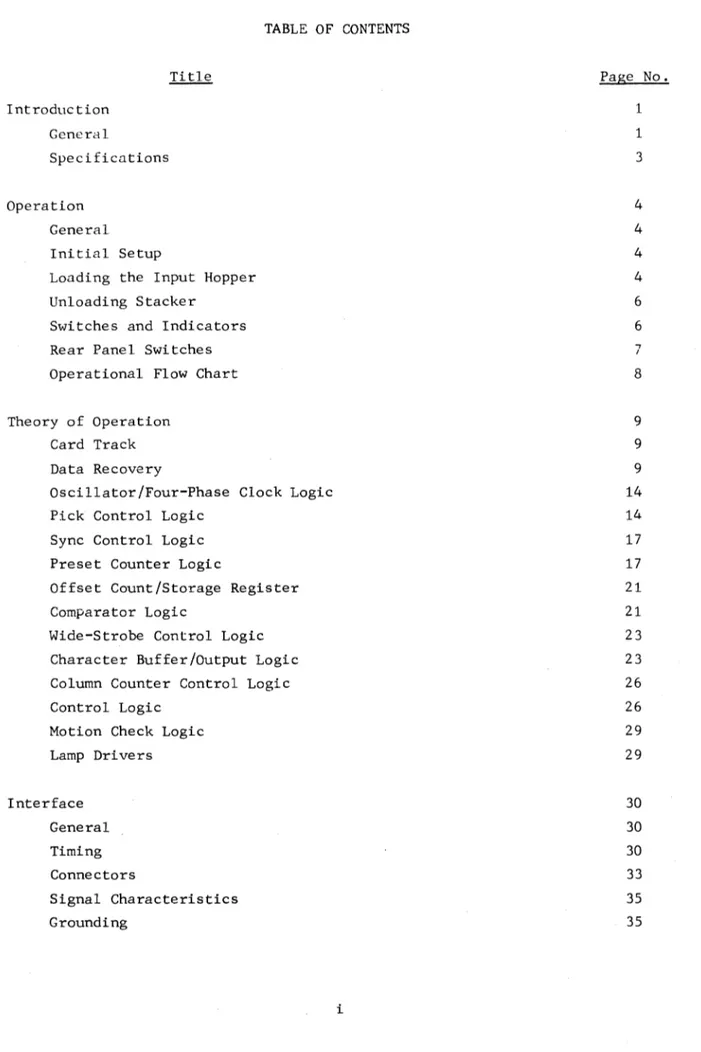
timing relationships. It is important to note that data is only guaranteed to be present from the trailing edge of the CSDS pulse to a point shortly before ST0C.
The guarantee period is different for each reader model and even though a gener-ous delay is guaranteed, it is good practice to accept the data as soon as offered by
-FROM
4-ct>
CLK LOGIC {4IB 4IA
I
FROM 4-4> CLK LOGIC
FROM COMPARATOR
LOGIC FROM
4-41
CLK LOGICCI
ENABLE
~
J
COLUMN
-
-~
CLOCK CLK 7-STAGE EOCC STORAGE ENABLEENABLE COUNTER AND DATA
GATE DECODE GATE STROBE
CONTROL
STct>D f(PRESETl
CI
MICROSECONDS
u-v
--i
I--
Z I MICROSECOND---i
r--
ZI MICROSECONDINDEX MARKER
STROBE CONTROL
IMST
- -
CSDSTO COLUMN COUNTER CONTROL LOGIC
TO INTERFACE LOGIC
"---' - - - . .
'---I~
~---,n,---~r
<pB
n
I
---..j
I--ZIP.SECI
: n
~~I
n,"""-~n",---STCPD
ENABLE
CSDS
a
CLKEOCC
IMST
__ _
....In:
/ I : ,I.n~
____
_
I
I
/IfJL
---+:~i
________
~/,~/----~~~---I
f4-
WIDE STROBEPE~IOD ~
!
II
--~:-~I
I~~/I~--~
______ _
I
I'
---~~---~;/~----~
I
"--~-~y I I I~---'"I--
TIMING DETERMINED BY MODEL ---.:~
6 MICROSECONDS_ ________________________ ~I I _________________ ___
I I
. NOTES:
OCR RESET
81 CR SET
STACK CHECK STACK SENSOR
CJ)-..
_._._-_.-STACKER ALARM DETECTOR INFRARED LIGHT
EMITTER
INFRARED LIGHT EMITTER .... Z III :. III > o ::I o II:
'"
..,
DARK ONE DETECTONE LIGHT DETECT
ONE DARK ONE LIGHT
TO CONTROL LOGIC
0 )
.. __ ._.-
CHARACTER BUFFEROUTPUT
DRIVERS TO EXTERNAL EQUIPMENT
EXAMPLE READ SENSOR OUTPUT
CSDS
RESET
...
I~_---
HOLE---·~~Ifoo~---
WEB~
I
~
I.
NO HOLE~
I
r---,
I I
STf#JC
-:::u:::=
I ,..SEC~
I--
Z7,..
SECU
II
I
CSDS
DATA LINE
INDEX MARK
DATA GUARANTEED t - - - - DATA GUARANTEED ---<-I
I--Z2,..SEC
__________
~rl~__________________
~rl~__ _
--1
~
6 MICROSECONDSNOTES-II) TIMING NOT SHOWN TO SCALE.
(2) THE SPACING BETWEEN ST4>C, THE DURATION OF CSDS, AND THE GUARANTEE PERIOD OF THE DATA DIFFERS DEPENDING ON READER MODEL. ;~~FNRG.TO.INTERFACE SECTION FOR SPECIFIC
Figure 13. Character Buffer Storage Logic Block Diagram
-the Index Mnrk. Either the leading or trailing edge of the Index Mark OM) m:1Y be used to accept the data. The data signals will have settled by the occurrence of 1M.
The ONE LIGHT and ONE DARK signals are derived if any ~ sensor goes Light or di1rk. These signals are sent to the Control logic where they are interrogated at the proper time (see figure 6) to establish that the card does not have leading or trailing edge tears (Dark Check) and that the sensor array is responding to its stimuli properly (Light and Dark Check) •
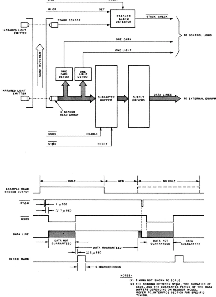
COLUMN COUNTER CONTROL LOGIC
The Column-Counter Control logic (figure 14) is initialized by GPR to begin counting the number of data columns read as the card moves past the read station. The seven-stage binary counter is triggered by ST~C, which is syn-chronized to the data column of a card. The counter decode gating recognizes OCR (pseudo-column 0) and 81CR (pseudo-column 81) to produce the two dark checks
(J2KS). This provides the dark check of the read station at the beginning and end of the card being read. The counter decode gating circuits also detect lCR (enable) and 81CR (disable) to control the Index Marker generation. The 84CR count recognition is used to initiate the Light Check and to indicate the end of the read cycle. This signal also re-establishes the readiness of the card reader to accept the next pick command (provided no alarm conditions have occurred for the card being processed) •
CONTROL LOGIC
The Control logic (figure 15) contains the error alarm detection circuits, ready-condition detect circuits, and pick control and gating circuits.
The Pick Check control circuits signal the fact that a card has been
FROM COMPARATOR
LOGIC
FROM WI DE - STROBE CONTROL LOGIC
FROM PICK CONTROL LOGIC
ST4ID
ST4»C
IMST
GPR +
i'lESET
GPR
OCR
ICR
IMST a 1M
81CR DCKS 84CR COUNTER DECODE
-84CR
- -
OCRTO CONTROL AND SYNC CONTROL LOGIC
7-STAGE
I
COUNTER ...GATING
BICR
}TO CONTROL LOGIC
COUNTERIOUTPUTS JI'
ICR. .·BI CR
INDEX MARKER CONTROL
!
I
.,..
"-I
DARK CHECK
STROBE DCKS
GATE
1M
-- ---
GPR + RESETTO INTERFACE EQUIPMENT·
TO CONTROL LOGIC
NOTE:
(I) TIMING NOT SHOWN TO SCALE.
(2) GPR OCCURS AT LEADING EDGE OF CARD.
--I
I'--~ B.33 MICROSECONDS~,~/--~{,~{---
~VARIABLE TIMING--I
~::::II MICROSECOND_~~R-t~~~~Jl"---84
---I
~ z 2 MICROSECONDS__
---Irl-i~~~~~~3~
II:
--I
~TIMING DETERMINED BY MODELI
---i
;-.-+1 -11/I
Z I MICROSEC::U:= 1 fI
I
I 1
I
:
I~I
:
I
-...j
\--TIMING DETERMINED BY MODEL I:
/~~J1BO
/( :---II~-I;
---I
~ 6 MICROSECONDS i f I/,~/---f.I--II'
-I
h
~/
I
I //
~Zl
MI[ROSECOND ,I
I II
I I I
_ _ --I' /~
n
Lfr
I,rt
/n
/I I'I },
_ _ _
~/
/-,----11 /-1---1'/-'---1"
I
r-" i f Ii ::::I I
MIC~6sECOND:::::U;=
Figure 14. Column Counter Control Logic Block Diagram
-FROM INTERFACE LOGIC {
FROM COLUMN CTR LOGIC {
FROM PICK CONTROL LOGIC
FROM HOPPER MICROSWITCH
PICK CONTROL LOGIC
FROM COLUMN { COUNTER LOGIC
FROM INTERFACE LOGIC
FROM CONTROL LOGIC CIRCUITS
FROM FRONT PAN EL
- -
RESET + POR-GPR + RESET POR
•
FROM COL. CTR. LOGIC• •
----
-ONE DARK LT CK
ONE LIGHT FROM PICK I PCR
READ CHECK CONTROL LOGIC
I
--
READYDCKS OK CK DETECT
CONTROL CONTROL
84CR LOGIC
I
--
STK LOGICPCK
r
I
I I I
STOP ..HCK
I
I
I I
I I---
RESET + POR--•
IF-HOPPER
-~
CHECK CONTROL
LT CK
t
I
LIGHT/DARKHi>'SW OK CK ERROR
I
DETECTPCK
--
PCK GATEOCR STK
iiCii
+
STACK ERROR
--
STK- -STACK DETECT LOGIC
RESET + POR
t
- - -
RESET + POR•
~
I
READY STOP STOP STOP
CONTROL
I
FROM CONTROL LOGIC CKTS LOGICREADY STOP SW
t
FROM SYNC CONTROL LOGIC RffiT PICK CI CONTROL AND FROM 4 -I/> CLK LOGIC GATING FROM COLUMN COUNTER LOGIC 84CR
FROM EXTERNAL EQUIPMENT PICK CMD
READY
READY
-READY
READ CHECK.
HCK HCK ERROR
f----
STK BUSY- -
PCLKTO EXTERNAL EQUIPMENT
a CONTROL LOGIC CIRCUITS
TO CONTROL LOGIC CIRCUITS
} ro
"""~ '''''~
} TO EXTERNAL EQUIPMENT
} TO
IN~ICATOR
DRIV"RSTO EXTERNAL EQUIPMENT
TO PICK CONTROL LOGIC
iillT FROM SYNC CONTROL LOGIC -'=:":"':--I~
RESET/POR GATE
RESET+ POR TO CONTROL LOGIC CIRCUITS AND PICK CONTROL LOGIC FROM 4-1/> CLK LOGIC _"":P"":O:';'R'---ie-"'l.,j
POR
TO CONTROL LOGIC CIRCUITS
NOTE'
TIMING NOT SHOWN TO SCALE
POR
=E~N~D_O~F~P~O~R~ _ _ _ _
~/~/---1/I,LI---i,I,II---f
II ,- ,..READY 1 IF NO ERRORS
' .. ---11/
II
II~/---G~~R GPR
,'---:---"1/
f----1
'---I
~
---l
~ TIMIN~I,VARIABLE II I I________ ... 1 7/ j r i
,1---BUSY
PICK CMD
I
--1
r--
8.~3 ,.,.SECCI
---~)1J1Jl;~~
----tu-Lr~f___lJlf1.Jlj_
----...j
, r - -
TlMI~G DETERMINED BY M,ODELi~;TCARDPICKED '~
PCLK
GPR
The Error Detect gate recognizes a data error condition from any of the
above detect circuits and provides an ERROR signal to the external equipment.
Simultaneously the particular alarm condition indicator on the card reader
front control panel is illuminated. The Hopper Check Control circuits utilize
the microswitch in the riffle cap to sense when the hopper is empty of cards. Another microswitch in the stacker follower assembly senses when the output
stacker is full of cards. Either of these conditions will generate the HCK
alarm.
The Stop Control logic detects the fact that the STOP pushbutton switch
on the card reader front control panel has been depressed or that a light/
dark check error has occurred to lower the READY line. The Ready Detect
control logic utilizes the fact that no alarm conditions exist to raise the
READY line for external program control and internal control use. The READY
line is lowered at the instant of error detection but the card reader operation
is not stopped until after the present card is processed completely.
MOTION CHECK LOGIC
The stack check sensor (see figure 13) is located at the exist of the
card track and detects that the tail of a card is clear of the card track
(hence, fully seated in the output stacker). The Stack Alarm logic is designed
to test that the stack sensor made a dark-to-light transition (i.e., track clear) between the time a 81CR signal occurs (card tail leaving the read
station) and the OCR signal of the next card. Should this transition not
have taken place, a STACK CHECK alarm is generated. This signal is combined with the Pick Check alarm to generate a MOTION CHECK alarm to the external
equipment should either condition occur. The card reader is stopped and the
READY line goes FALSE.
LAMP DRIVERS
The lamp drivers amplifiers provide the current drive for the alarm
indi-cators on the front control panel. The LAMP TEST input to the lamp driver circuits enables the output drivers for all indicators simultaneously,
INTERFACE
GENERAL
This section covers the interface between the M Series punched card
readers and the equipment into which it transfers data.
TIMING
In interfacing the M Series card readers to an external system or card
reader controller, the designer should appreciate that three separate
cate-gories of interface signals are being dealt with. The first are the signals which control and report the status of card processing, the second are the data
signals themselves with their associated index marks, and the third are the
various alarm signals provided. In the description following, the designer should refer to the timing diagram shown in figure 16.
Pick Control
The PICK COMMAND initiates the card read cycle, and depending upon its duration, the card reader will either continuous run or operate in a
card-at-a-time mode. This signal can be presented to the reader at any time, but the
reader will only accept it when the READY line is TRUE. The READY Signal
indi-cates that the card reader is cleared of errors and is ready to receive a PICK
COMMAND from the external program control. A visual indication of the READY
line is the green RESET indicator on the front control panel.
The conditions which must be present for the READY line to be TRUE are:
1. Power applied and the 3 second run-up completed. 2. The input hopper has been loaded.
3. Depressing the RESET pushbutton switch will bring the READY line TRUE.
Should all of the above conditions be satisified, the presence of a PICK
COMMAND signal will generate the PICK pulse to the picker solenoid. The first card is introduced into the card track, and after a delay (see A, figure 16),
the leading edge will arrive at the read station. The BUSY signal will go TRUE
as soon as the leading edge of the card enters the read station.
To initiate the card pick cycle, the PICK COMMAND must be present for at
least 1 microsecond (us) concurrently with the READY signal. Once the pick
READY
PICK COMMAND
PICK (SOLENOID)
BUSY
DATA LINES
INDElI MARKS
BUSY
DATA LINES
BEGIN CARD READ CYCLE
I----
TIME VARIABLEu
DATA COLUMN I COLUMN 2
GUARANTEED GUARANTEED
---<l~I----C SHADED AREA NOT GUARANTEED
I---
2fLSECINDEX MARKS
__________
~n~·________________
~n~________ _
PICK ( SOLENOID)
BUSY
DATA COLUMN 80 DATA L I N E S . GUARANTEED
-11-
',m
D.1
I
--l~
I fL SECI
i
I
-I
INDEX MARKS ~~ ____________________________________________________ ~ __________________________ __
f--I· - - - - -E
NOTE'
WAVEFORMS NOT SHOWN TO SCALE.
Figure 16.
MODEL M 200 M300 101600 1011000 MII!OO A (MIN) 24 24 24 IS 14 M SEC
END CARD READ
B
c
6250 1314 2600 435 2600 435 1860 240 1120 240
p.·SEC p.SEC CYCLE
o
2014 870 870 478 405P. SEC
E 8050 102,660 3480 1910 (529
P. SEC
CARD PICK CYCLE 200 200 100 60 50
M SEC
Standard Interface Timing for M Series Readers