5
III
March 2017
Technology (IJRASET)
Reduction of Common Mode Voltage in Three
Level Diode Clamped Inverter
Shiwani Rasekar1, Heena Sheikh2
1,2
Electrical-Electrical Engineering Department, Gondwana-Gondwana University
Abstract: In this paper, an approach to reduce common mode voltage (CMV) at output terminal of the inverter using simple
sinusoidal PWM technique is proposed. Multilevel inverter (MLI) is more suitable in high & medium power application, CMV is produced at the time of operation in output terminal of inverter. This paper realizes the implementation of PD-SPWM technique to reduce CMV for three level diode clamped inverter (DCMLI). A good transaction between the quality of the output voltage & the magnitude of CMV is achieved in this paper. The main purpose of the paper is to study and implement hardware circuit of three level DCMLI using MOSFET’s. However, the output voltage is smoother with a three level converter. Simulation & experimental result presented to confirm the effectiveness of the proposed technique to control CMV.
Keywords: diode clamped MLI, common mode voltage, sinusoidal PWM technique, PD technique.
I. INTRODUCTION
Multilevel inverter (MLI) come to attention of researchers as soon as it was proposed by Nabae A in 1981. In the area of high power application multilevel inverter is a first choice where the demand is increasing & produced energy does not cope with the increasing demand. To obtain quality output voltage & current waveform with minimum ripple content, two level inverter require high switching frequency along with various PWM strategies. Two level inverter may not suit for high voltage application because of poor quality output. MLI has drawn tremendous interest in the power industry application. Output of two level inverter is modified by increasing number of voltage level in the inverter without requiring higher rating an individual device can increase the power rating. Multilevel inverter consist of number of thyrister switches depends upon levels used in the inverter. Now a day's thyrister switches replace by SCR's, BJT's, MOSFET's & IGBTE's depending upon respective advantages. By switching action of the inverter switches staircase output is generated which is also called as multilevel output. As the number of voltage level increases the harmonic content of output waveform decreases significantly. Output generation by switching action results in common mode voltage (CMV) which are essentially zero sequence voltages superimposed with switching noise which will appear at rectifier, inverter & motor terminals. If not minimized then they appear on the stator winding with respect to ground results in motor life expectancy is shortened. As the number of voltage level increases the synthesized output waveform has more steps which produce a staircase wave that approaches a desire waveform & harmonic distortion of the output waveform decreases approaching zero as no of level increases.
Fig 1: general block diagram of ac-dc-ac vsi or csi fed asd.
Technology (IJRASET)
II. BACKGROUND
A. Three Level Diode Clamped Inverter
[image:3.612.206.403.160.331.2]In high voltage & high power application diode clamped multi-level inverter (DCMLI) become a research hotspot. Multi level inverter is preferred in between three to nine level inverters. As the number of voltage level increases total harmonic distortion is reduced. Three level inverter is shown in diagram below.
Fig 2: Schematic diagram of three phase, three level diode-clamped inverter.
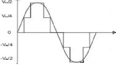
Three phase diode clamped MLI have three legs with common DC bus, this DC voltage is subdivided into switching capacitors. Each diode has to block the voltage equal to number of switching above it times the supplied DC voltage. Basically one leg of DCMLI consist of 'M-1' capacitors & 'M-2' clamping diodes where 'M' is the total voltage levels & total number of switches are 2(M-1), in the three level inverter number of switches used are 12, for the operation in numbering order of Sa1, Sa2, Sb1, Sb2, Sc1, Sc2, Sa1', Sa2', Sb1', Sb2', Sc1' & Sc2'. Dc bus consist of two capacitors C1 & C2, six diodes are used two for each leg. In DCMLI diode is used as clamping device to clamp the dc bus voltage so as to achieve staircase output voltage as shown in the diagram.
Fig 3: Staircase output of the three level inverter.
B. Common Mode Voltage
Common mode voltage is defined as the voltage between neutral point of the load & system ground. It may also defined as the voltage between neutral point of the load & dc midpoint given diagram shows generalized drive system , where Vag, Vbg & Vcg are the voltages between ground to phase & Vng is the voltage between neutral point of the motor and system ground. i. e. CMV & it is given as:
CMV = Vng = (Two level inverter)
[image:3.612.206.403.453.563.2]Technology (IJRASET)
CMV= Vng = (Five level inverter).
[image:4.612.200.430.171.316.2]Output of the inverter is not purely sinusoidal but square wave (discrete), hence sum of the instantaneous value is not zero & develops common mode voltage. Meanwhile in purely sinusoidal three phase system sum of the instantaneous voltage is zero hence CMV is zero. Neutral point voltage variation results in generation of common mode voltage three times the fundamental frequency. If common mode voltages are not reduces they results in bearing failure of the motor connected as load in output terminal.
Fig 4: Three phase VSI inverter with Induction motor connected as a load.
III. CMVCONTROLSTRATEGIES
Control strategies for common mode voltage can be classified as given below
Using some extra hardware circuitry such as isolation transformer, active passive filter, common mode choke & dual bridge inverter etc.
Using modification in control strategy such as space vector PWM technique (SVPWM) & sinusoidal PWM technique(SPWM). In the first method common mode voltage is minimized by selecting proper rating of the chock, but the main issue is that the total harmonic distortion(THD) increases with controlling CMV.
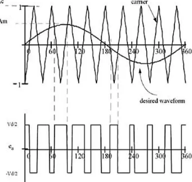
Fig 5: Sinusoidal pulse width modulation technique
[image:4.612.208.403.440.625.2]Technology (IJRASET)
proportion to the amplitude of sine wave evaluate at the centre at the same pulse. The distortion & lower order harmonics are reduced significantly. The gating signal generated by comparing sinusoidal reference signal with triangular carrier wave. When instantaneous value of the sine reference is greater than the triangular carrier wave then the output is at +Vdc & when the reference signal is less than the carrier signal then the output is at -Vdc.
Different SPWM technique can be classified as: Phase disposition method
Phase shifted method
Phase opposition disposition method.
A. Phase Disposition Method
[image:5.612.196.417.249.379.2]Phase disposition method based on the comparison of sinusoidal reference waveform with triangular carrier waveform, all the carrier waveform have same frequency and amplitude & all the carrier waves are in phase with each other. If 'M' is the number of voltage level in inverter then 'M-1' carrier signals are used to generate voltage levels.
Fig 6: Phase disposition PWM technique.
IV. EXPERIMENTALRESULTS
A. Simulation Results
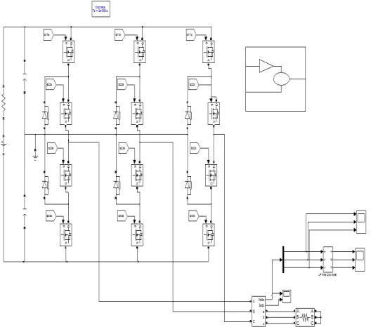
Below figure shows the simulation diagram of the proposed inverter. The circuit is designed in Matlab/simulink and the generation of pulses has been made by comparing every carrier wave with the sine wave and the resultant pulses has been given to the appropriate switches to produce the three level staircase waveform.
[image:5.612.175.439.460.693.2]Technology (IJRASET)
[image:6.612.199.413.128.287.2] [image:6.612.198.415.318.485.2]Diagram below shows experimental results of three level diode clamped inverter common mode voltage reduction by PD-SPWM technique with & without filter. Fig 9 shows output of inverter which is staircase wave. Sinusoidal waveform obtained after filtering inverter output.
[image:6.612.202.411.517.698.2]Fig 9: Output waveform of proposed MLI using PD technique.
Fig 10: Filtered output waveform of proposed MLI
Technology (IJRASET)
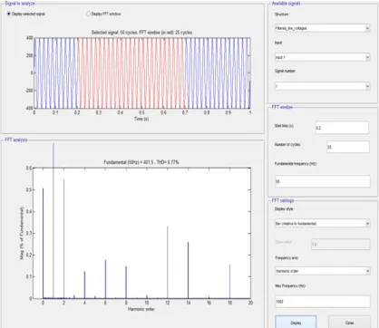
The total harmonic distortion (thd) of any waveform is defined as the closeness to the fundamental wave shape. FFT analysis is done to determine the Thd of the output waveform.
B. Hardware Explanation
The various sections of hardware are explained below.
1) Supply Section: Full wave bridge rectifier fed by step down transformer which is supplied with 230V input power. Rectifier converts 12V AC transformer output into 12V DC. Regulator IC 7805 regulates this voltage to 5V and keeps it constant to drive microcontroller IC.
2) Microcontroller Section: An AC input voltage is fed to a three phase diode bridge rectifier through step-down transformer in order to produce dc output voltage across a capacitor filter. A filter removes the ripple contents present in the dc output voltage. A pure output is applied to multilevel inverter through capacitor filter. The multilevel inverter has 12 MOSFET switches that are controlled in order to generate an ac output voltage from the dc input voltage. PIC76F877A IC is given with opt coupler COSMO1010 to provide electrical isolation between input & output also to protect control circuit from potentially fatal power surge from the power circuit.
3) Amplifier section: Voltage through microcontroller sends to amplifier section consists of transistor BC547 & resistor.
4) DCMLI Section: MOSFET driving IC IR2110 supplied Vds to 12 MOSFET’s in order to generate an ac output voltage. At 230V, 50 Hz input signal 7V output voltage for each phase is obtained.
Implementation of hardware includes the procedure of layout planning for PCB, Artwork, painting, etching, drilling mounting of various components like resistor, capacitor , MOSFET’s and IC’s after mounting finally I soldered all the component.
Fig 12: Hardware circuit and output of of three level DCMLI
All the outputs are of push pull type. Input & Outputs are protected against electrostatic effects in wide variety of device handling situation. However to be totally safe, it is desirable to take handling precaution into account.
V. CONCLUSION
The paper provides comprehensive analysis on the three level diode clamped inverter, which is also known as neutral point clamped (npc) inverter. The diode clamped multilevel inverter (DCMLI) provides multiple voltage level through connection of phase to series capacitors. The use of the three level inverter reduces the harmonic components of the output voltage compared with the two level inverter at the same switching frequency. This system is suitable for high voltage and high power application.
REFERENCES
[1] Xiaoming Yuan, member, IEEE & Ivo babri, senior member IEEE, "Fundamental of new diode clamping multilevel inverter," IEEE transaction on power electronics, vol 15, no. 4, july 2000.
[2] F. Wang, "Sine triangle versus space vector modulation for three-level PWM voltage source inverters," IEEE Transactions on Industry Application, vol. 38, no.2, pp.500-506,2002.
Technology (IJRASET)
[4] Chenggang Mei, Juan Carlos Balda, and William P. Waite, "Cancellation of common mode voltages for induction motor drives using active method ," IEEE Trans. Energy Conversion, Vol.21, pp. 380-386, Jun. 2006.
[5] R. S. Kanchan, P. N. Teckwani and K. Gopakumar," Three level inverter scheme with common mode voltage elimination and dc link capacitor voltage balancing for an open-end winding induction motor drive," IEEE Transaction on power electronics, vol.21, no. 6, pp. 1676-1683,2006.
[6] A. Videt, P. Le Moigen, N. Idir P. Baudesson, and X. Cimetire, "A new carrier-based PWM providing common mode-current reduction and DC-bus balancing for three-level inverter," IEEE Transaction on Industrial Electronics, vol. 54, no. 6, pp.3001-3011,2007.
[7] Jose Roriguez Steffen Bernet, Bin Wu, Joege O. Pontt and Samir Kouro, " Multilevel voltage -source-converter topologies for industrial medium voltage drive", IEEE Trans. Indl. Electron, Vol. 54, No. 6, pp. 2930-2944, Dec. 2007.
[8] Pradyumn Chaturvedi, Shailendra & pramod Agrawal,"Carrier based CMV control techniques in three level diode clamPD inverter," Advances in power electronics, 2012, pages 12.
[9] Z. Zhao, Y. Zhong, H. Gao, L. Yuan and T. Lu, "Hybrid selective harmonic elimination PWM for common mode voltage in three level neutral point clamped inverter for variable speed induction drives," IEEE Transaction on power electronics, vol. 27, no. 3, pp. 1152-1158,2012.
[10] Jayant M Parkhi, R.K.Dhatrak, "Reduction of common mode voltage in AC drive using MLI," IJERA, vol. 3, isuue 4, Jul- Aug 2013, pp. 212-218.
[11] Akash A. Chndekar, R.K.Dhatrak, Z.J.Khan, "Modelling & simulation of diode clamped multiinverter fed three phase induction motor for CMV analysis using filter," IJAREEIE, vol.2, issue8, Aug 2013.
[12] C. Bharatiraja, K.V.R.S.. Prakara Rao, Dr. S. Jeevanthan, "Reduction of common mode voltage in three level neutral point diode clamped multilevel inverter using space vector pulse width modulation, " IJCEEE, vol 1, issue 2, Dec 2013.
[13] M. S. Raghuvendra Reddy, G. Sri. Harsha, B. Nishanth, E. Sai. Pratik Reddy, "Common mode voltage reduction in DCMLI," IJETT, vol 11, No. 2, May 2014. [14] Darshan Prajapati, Vineetha Ravindra, Jil sutaria, Pratik patel, "A comparitive study of three phase 2 level VSI with 3 level & 5 level diode clamped multilevel
inverter," IJETAE, vol 4, issue 4, april 2014.