Nanoscale
C. T. Stoppiello,a J. Biskupek,b Z. Y. Li,c G. A. Rance,a,d A. Botos,a R. M. Fogarty,e R. A. Bourne,f J. Yuan,g
K. R. J. Lovelock,h P. Thompson,i,j M. W. Fay,d U. Kaiser,b T. W. Chamberlain,f A. N. Khlobystova,d The preparation of inorganic nanomaterials with a desired structure and specific properties requires the ability to strictly control their size, shape and composition. A series of chemical reactions with platinum compounds carried out within the 1.5 nm wide channel of single-walled carbon nanotubes (SWNTs) have demonstrated the ability of SWNTs to act as both a very effective reaction vessel and a template for the formation of nanocrystals of platinum di-iodide and platinum di-sulphide, materials that are difficult to synthesise in the form of nanoparticles by traditional synthetic methods. The stepwise synthesis inside nanotubes has enabled the formation of Pt compounds to be monitored at each step of the reaction by aberration-corrected high resolution transmission electron microscopy (AC-HRTEM), verifying the atomic structures of the products, and by an innovative combination of fluorescence-detected X-ray absorption spectroscopy (FD-XAS) and Raman spectroscopy, monitoring the oxidation states of the platinum guest-compounds within the nanotube and the vibrational properties of the host-SWNT respectively. This coupling of complementary spectroscopies reveals that electron transfer between the guest-compound and the host-SWNT can occur in either direction depending on the composition and structure of the guest. A new approach for nanoscale synthesis in nanotubes developed in this study utilises the versatile coordination chemistry of Pt which has enabled the insertion of the required chemical elements (e.g. metal and halogens or chalcogens) into the nanoreactor in the correct proportions for the controlled formation of PtI2 and PtS2 with the correct stoichiometry.
Introduction
The development of new methodologies for the controlled arrangement of molecules and atoms into highly ordered arrays is vitally important for harnessing the functional properties emerging at the nanoscale due to the effects of confinement, which are essential for catalytic, electronic and biomedical applications. The cylindrical internal cavity of single-walled carbon nanotubes (SWNTs) provides an effective template for control of the exact positions and orientations of the molecules and atoms and has been successfully applied to the construction of nanoscale architectures from a variety of metals, organic molecules,1-3 and inorganic compounds.4-9 A
striking example of the power of this technique was reported by Chuvilin et al. who demonstrated that sulfur-terminated graphene nanoribbons, practically impossible to fabricate by synthetic chemistry routes, can be spontaneously formed from inexpensive, readily available precursors, such as tetrathiafulvalene, in one step within SWNTs.10, 11 More recently, very narrow double-walled carbon
nanotubes have been demonstrated as effective containers for templating the important, but still elusive, allotrope of carbon, carbyne.12 Shi et al. demonstrated that at high temperature the host
nanotube can template the formation of this new allotrope of carbon and protect it from undesired side reactions, thus paving the way for the first bulk production of carbyne. These examples clearly demonstrate the intrinsic ability of the SWNTs to direct chemical reactions and control the dimensionality of the products formed inside nanotubes, where the product structure is crucially determined by the internal diameter of the nanotube.
Low-dimensional inorganic materials, including transition metal chalcogenides, are currently of particular interest due to the fact that their semiconducting electronic properties can be precisely tuned by shaping their structures into nanoribbons, in an analogous fashion to graphene.13 While the host-nanotube can control the dimensions of
the inorganic structure, control of the stoichiometry is typically achieved by immersing open SWNTs into a molten inorganic compound with the desired, predetermined chemical composition, so that the nanotube becomes filled with cations and anions in the correct ratio due to capillary forces. A now ubiquitous technique, it has led to the encapsulation of many inorganic compounds, such as lanthanide halides,14 potassium iodide,15 cobalt iodide,16 tin
telluride,17 and barium di-iodide,6 yielding nanostructures with
well-defined composition and morphology, and physical properties often different to those found in the bulk. However, the need to melt inorganic compounds in this method imposes severe limitations on the choice of encapsulated materials, as many important inorganic materials, such as metal sulfides, decompose before melting or melt at extremely high temperature, e.g. the melting point of MoS2 is
1185 °C.
The direct synthesis of inorganic compounds inside nanotubes can offer an attractive alternative which may significantly broaden the scope of inorganic compounds that are confined to the nanoscale. The nanotube in this case acts simultaneously as a nanoscale reactor and a template for controlling the dimensions of inorganic structures. Inorganic synthesis inside nanotubes has been successfully applied by Eliseev et al. to the synthesis of CdS@SWNT by treating pre-encapsulated CdI2, inserted into nanotubes from the
molten phase, with sulfur at high temperature.18 This elegantly
avoids the problem that bulk CdS has a melting point of 1750 °C,
a School of Chemistry, University of Nottingham, University Park, Nottingham NG7 2RD,
U.K.
b Central Facility for Electron Microscopy, Ulm University, Albert-Einstein-Allee 11, Ulm
D-89081, Germany.
c Nanoscale Physics Research Laboratory, School of Physics and Astronomy, University of
Birmingham, Birmingham B15 2TT, U.K.
d The Nanoscale and Microscale Research Centre, University of Nottingham University
Park, Nottingham NG7 2RD, U.K.
e Department of Chemistry, Imperial College London, London, SW7 2AZ, U.K.
f Institute of Process Research and Development, School of Chemistry, University of Leeds,
Leeds LS2 9JT, U.K.
g Department of Physics, University of York, Heslington, York YO10 5DD, U.K. h Inorganic Chemistry Laboratory, University of Oxford, South Parks Road, Oxford, OX1
3QR, U.K.
i Department of Physics, University of Liverpool, Liverpool L69 7ZE, U.K.
j XMaS CRG, European Synchrotron Radiation Facility, 38043 Cedex, Grenoble, France.
precluding the molten phase filling of this material. Similarly, the formation of low-dimensional MS2 (M = Mo,19 W20) in multi-walled
carbon nanotubes has been demonstrated by Wang et al. via the decomposition of molecular complexes highlighting the further potential for tailoring bespoke semiconducting inorganic materials with nanoscale precision. Recently, we demonstrated the formation of MS2@SWNT (M = Mo, W) via a metal-iodide intermediate, and
showed that the SWNT acts not only as a template to restrict the morphology of the MS2, but also as a reservoir of electrons to
stabilise the reaction intermediate.21
In this study, we evaluate carbon nanotubes as nanoreactors in stepwise and one-pot inorganic syntheses, highlighting the advantages and limitations of the different approaches. Using the compounds of platinum as models, we outline a new strategy for the fabrication of inorganic nanomaterials with controlled structure and composition. Conducting the chemical transformations inside the host-nanotube allows for the structural determination of the reaction products with atomic precision by aberration-corrected high resolution transmission electron microscopy (AC-HRTEM) and aberration-corrected scanning transmission electron microscopy (AC-STEM), while our unique approach based on cross-correlation of fluorescence-detected X-ray absorption spectroscopy (FD-XAS) and Raman spectroscopy applied at each stage of inorganic synthesis in carbon nanotubes enables determination of the exact oxidation state of the metal (Pt) in inorganic compounds formed inside nanotubes and the vibrational properties of the host-nanotube respectively. This methodology enables changes in host-guest interactions from one stage of the inorganic synthesis to another to be monitored by multiple techniques for the first time, providing a systematic understanding of the electron transfer between the nanoreactor and encapsulated compound during all stages of the formation process.
Results and discussion
The stepwise formation of inorganic materials in SWNTs can be achieved by selecting an appropriate metal precursor, i.e. small volatile metal complexes consisting of the required metallic element for the desired inorganic material, and inserting them into the nanotube (figure 1a), followed by thermal treatment to remove the volatile ligand from the nanotube cavity (figure 1b), with the sequential addition of a non-metallic element which reacts with the metal to form the desired inorganic compound. If necessary, more reaction steps can be added to convert the inorganic compound to another product (figure 1d).
To explore and evaluate this approach for inorganic synthesis in SWNTs, platinum acetylacetonate, Pt(acac)2 was inserted into
SWNTs from the gas phase, with the excess removed from the
exterior of SWNTs by applying a selective CH2Cl2 washing
technique,22 leaving only Pt(acac)2 molecules encapsulated within
the nanotube, Pt(acac)2@SWNT. The LIII edge of Pt (measured in
FD-XAS) can be used as a probe of oxidation state, this edge results from excitations between 2p3/2 and 5d states. Higher Pt oxidation
states (lower electron density) stabilise 2p3/2 orbitals, and hence lead
to larger Pt LIII edge energies.23 Furthermore, the characteristic G
band, ubiquitously observed in the Raman spectra of graphitic nanostructures, and caused by vibrations of carbon atoms of E2g
symmetry in an extended lattice, is sensitive to strain and curvature of the nanotube, and can be used to measure any electron transfer from the nanotube to guest molecules.24 A red shift is indicative of
electron transfer from the intercalant to the SWNT, and a blue shift is indicative of electron transfer from the SWNT to the intercalant.
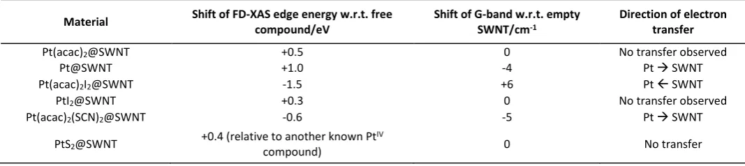
FD-XAS of Pt(acac)2@SWNT shows a slight increase in the Pt LIII edge
energy relative to that of a Pt(acac)2 control sample (supporting
information, table S-1) indicating a small reduction of electron density on the metal centre of Pt(acac)2 inside the nanotubes (figure
2a); however, Raman spectroscopy (figure 2b) shows no shift in the G-band of the SWNT suggesting little or no charge transfer between the guest and the nanotube upon encapsualtion.25 Heating
Pt(acac)2@SWNT under argon at 500 oC for one hour resulted in the
decomposition of Pt(acac)2 and the release of metallic Pt into the
[image:2.595.318.564.346.461.2]SWNT cavities in the form of cylindrical nanoparticles with an average length of 1.5 nm and diameter of 1.0 nm as confirmed by TEM imaging (figure 2c inset, see SI file section 3d for AC-HRTEM images). The formation of small metallic nanoparticles rather than a
Table 1: Shifts of the Pt LIII FD-XAS edge energy for the different platinum materials in SWNTs with resepect to (w.r.t.) their free state, and
shifts in the G-band in the Raman spectra of nanotubes filled with different platinum materials w.r.t. that of empty SWNTs.
Material Shift of FD-XAS edge energy w.r.t. free
compound/eV
Shift of G-band w.r.t. empty
SWNT/cm-1
Direction of electron transfer
Pt(acac)2@SWNT +0.5 0 No transfer observed
Pt@SWNT +1.0 -4 Pt SWNT
Pt(acac)2I2@SWNT -1.5 +6 Pt SWNT
PtI2@SWNT +0.3 0 No transfer observed
Pt(acac)2(SCN)2@SWNT -0.6 -5 Pt SWNT
PtS2@SWNT +0.4 (relative to another known Pt IV
[image:2.595.42.576.654.773.2]compound) 0 No transfer
continuous metal nanowire is determined by the limited number of metal atoms available in the nanotube, the stabilising effect of the nanotube and the release of gaseous ligand fragments upon heating, as was reported previously for W, Re and Os nanoparticles formed using similar conditions.26 The energy of the Pt L
III edge in Pt@SWNT
is increased significantly relative to bulk metallic platinum.
Simultaneously a small but measurable red shift of the G band in the Raman spectrum of the host-nanotubes, relative to empty nanotubes is observed, confirming that some electron transfer takes place from metallic Pt to SWNT in the Pt@SWNT material, which correlates with the FD-XAS (table 1). An alternative explanation is the formation of PtO2, but the metallic nature of the Pt nanoparticles,
rather than Pt carbide or oxides phases was also verified by careful comparison of the interatomic spacings in the individual
nanoparticles (dPt-Pt = ca. 0.26 nm) observed in AC-HRTEM which are
closer to Pt metal in a face centred cubic crystal (SI file section 3d).
In the next step, Pt@SWNT was treated with iodine vapour (figure 1b) leading to the direct synthesis of platinum iodide inside nanotubes, PtI2@SWNT, from the constituent elements (figure 2 d,
inset). Raman spectroscopy shows that the G-band of the host-nanotube in PtI2@SWNT returns to a similar position to that of
empty SWNTs, and FD-XAS shows that the energy of the Pt edge of PtI2@SWNT is similar to that of known PtII complexes (table 1), with
both methods agreeing that no electron transfer takes place between the nanotube and charge-neutral compound PtI2, which
contrasts with the observed Pt to SWNT electron transfer in Pt@SWNT as described above, or SWNT to iodine electron transfer described for I2@SWNT in the literature.25 The addition of H2S to
PtI2@SWNT led to the transformation of platinum iodide to the
platinum sulfide compound PtS2@SWNT (figure 1d) which in a
similar fashion to the iodide exhibits no electron transfer with the nanotube as the position of the G-band observed in the Raman spectrum of PtS2@SWNT coincides with that of empty SWNTs. This
is in agreement with FD-XAS showing a Pt excitation edge energy similar to that of known PtIV complexes (table 1), thus confirming a
charge-neutral PtS2 material inside the nanotube. This series of
chemical transformations inside carbon nanotubes clearly illustrates that stepwise inorganic synthesis involving transformations of a metal complex to metal nanoparticles, to metal iodide and to metal sulfide can be achieved in SWNTs with each stage verified by TEM, as well as FD-XAS and Raman spectroscopy revealing the nature of the interactions between the inorganic compounds and the host-nanotube.
In a separate experiment, both Pt(acac)2 and I2 were encapsulated
in SWNTs simultaneously, from the gas phase followed by heat treatment of the encapsulated molecules (Pt(acac)2 + I2)@SWNT
that triggers a chemical reaction between Pt(acac)2 and I2 to form
PtI2@SWNT in one step, which is analogous to a popular one-pot
synthetic approach in preparative chemistry in the absence of SWNTs. This platinum iodide appears to be identical to the same compound formed in the stepwise process above, which clearly indicates the advantages of the one-pot synthesis in nanotubes, allowing for the bypass of several stages of the stepwise approach,
i.e. Pt(acac)2 insertion and thermal decomposition, followed by I2
insertion into SWNTs. While both of these approaches appear to be effective in controlling the dimensions of inorganic nanostructures, being strictly defined by the diameter of SWNTs, detailed analysis of the elemental composition of the inorganic products reveals a problem of stoichiometry control. Unlike organic molecular compounds, inorganic materials have a capacity for non-stoichiometric ratios of the constituent elements, which is evident from energy dispersive X-ray (EDX) analysis indicating that the materials synthesised inside nanotubes in both approaches have a non-stoichiometric ratio of metal and halogen/chalcogen, (SI file, section 5). Specifically, the content of iodine in PtI2@SWNT appears
to be consistently higher than predicted for PtI2 (figure 2d), and
traces of iodine still remain present in the nanotubes even after conversion of PtI2@SWNT to PtS2@SWNT (figure 2e). This
observation clearly highlights the challenge of controlling the correct proportions of reactants in nanotubes: I2 is more volatile than
Pt(acac)2 and has a lower vapour pressure which means that it will
always be loaded into the nanotube in excess of the Pt precursor, thus making the removal of extra iodine difficult, even after platinum iodide is transformed into platinum sulfide (figure 2e). As even a
Figure 2: a) FD-XAS spectra showing the Pt LIII edge of materials in
SWNTs prepared using a stepwise approach compared to that of bulk Pt(acac)2. A smoothed line is overlaid on the raw data (black)
for each material; b) the derivative of the FD-XAS spectra shown in (a); the dashed line denotes the Pt LIII edge energy of bulk Pt(acac)2
and shows how this energy varies for different Pt materials within the SWNT; c) Raman spectra showing how the G band of the nanotube shifts depending on the encapsulated material. The dashed line denotes the position of G band of the empty SWNT for reference, the encapsulation of molecular species (Pt complexes or I2) leads to electron transfer between the nanotube and guest;
however, the encapsulated PtX2 (X = I or S) compounds exhibit no
change in G-band meaning that no charge transfer is taking place. d) an EDX spectrum of Pt@SWNT, a low magnification TEM image (the white arrows showing Pt) of the sample is shown inset. The O is from defects in the SWNT; e) an EDX spectrum of PtI2@SWNT
formed using the one-pot method. An excess of iodine is present in the sample. Inset is a TEM image showing clusters of Pt atoms (white arrow) and I atoms (red arrow) within the SWNT; and f) an EDX spectrum of PtS2@SWNT formed from the treatment of
PtI2@SWNT with H2S. Traces of iodine are still present in the
sample. Inset is a TEM image of PtS2@SWNT formed by the
transformation of PtI2@SWNT. In agreement with the EDX
[image:3.595.46.287.144.424.2]small deviation from the exact stoichiometric composition causes drastic effects in the physiochemical properties of inorganic materials, such as in the case of diamond doping with N, or boron nitride doping with C, effective control of the ratios of the elements is of paramount importance in inorganic synthesis at the nanoscale.27, 28
A solution to this challenge can be found by designing a molecular precursor where the elements are present in the desired stoichiometric ratio for a specific inorganic product, which can then be encapsulated and converted into the inorganic material in SWNTs in a one-pot-one-reactant synthesis (figure 3). The advantage of such an approach is that it involves a single step and the stoichiometric ratio of the metal and halogen/chalcogen components in the material formed can be carefully tuned. The use of coordination compounds of transition metals offers excellent potential for the control of the composition and stoichiometry of the reactants. For example, the coordination environment of four-coordinate Pt complexes, such as Pt(acac)2, can be expanded to six-coordinate by
appending two extra ligands to the axial positions, which can carry the correct amounts of the desired non-metallic element. For example, the addition of two iodide or two thiocyanate ligands that occupy the two axial positions in the octahedral complex of Pt allows fixing of the ratio of metal to halogen or chalcogen to 1:2 thus ensuring the correct stoichiometry of the inorganic compound formed inside the nanotubes (figure 3). To illustrate the principle of one-pot-one-reactant synthesis in nanoreactors, we prepared the molecular precursors trans-bis(acetylacetonato)di-iodoplatinum and
bis(acetylacetonato)di-thiocyanatoplatinum containing Pt:I (1:2) and
Pt:S (1:2) respectively by reacting Pt(acac)2 with I2 to give Pt(acac)2I2,
and then reacting Pt(acac)2I2 with AgSCN to afford Pt(acac)2(SCN)2,
using previously reported methods (scheme 1).29, 30
Scheme 1: The formation of Pt(acac)2I2 and Pt(acac)2(SCN)2 from
Pt(acac)2.
The resultant Pt(acac)2X2 (X = I, figure 3a; X = SCN, figure 3b)
compounds were added to SWNTs and sealed in an ampoule under vacuum (10-5 bar). Heating at a temperature slightly above the
sublimation points of the platinum complexes allowed the precursor molecules to penetrate the open ends of the nanotubes and become encapsulated. The excess material was removed from the nanotube surface by washing with CH2Cl2, leaving only molecules inserted in
the nanotubes.Interestingly, the encapsulation of Pt(acac)2I2@SWNT
led to a significant reduction in the absorption energy of the Pt LIII
edge indicative of an increase of electron density onto the Pt centre as compared to free Pt(acac)2I2 (figure 4a), which is complimented by
a significant blue shift of the Raman G-band of the host SWNT (figure 2b), implying electron transfer from the nanotube to the guest molecule which has not be observed for any other Pt compounds in this study. In contrast, Pt(acac)2(SCN)2@SWNT showed a decrease in
the Pt edge energy in the FD-XAS (figure 4b) and a red shift of the nanotube G band (figure 2b), indicating that the electron is transferred in the opposite direction to the previous complex, i.e. from Pt(acac)2(SCN)2 to SWNTs. A simple thermal treatment led to
the facile transformation of the molecular precursors to the desired inorganic structures, PtI2@SWNT and PtS2@SWNT (figure 3) with the
nearly stoichiometric 1:2 metal to halogen/chalcogen composition, as confirmed by EDX spectroscopy (figures 4c, d, SI section S5).
While the new one-pot-one-reactant approach clearly enabled a precise control of the stoichiometry, it is essential to verify the atomic structure of the inorganic compounds formed in this method, to ensure that the new molecular precursors still deliver inorganic materials with well-defined atomic structures. AC-HRTEM is one of the most direct tools for the structural characterisation of inorganic materials formed within SWNTs, as the precise atomic composition and any distortions in the crystal lattice can be clearly visualised to determine the effects of nanoscale confinement.20, 31, 32 AC-HRTEM
of the PtI2@SWNT sample prepared by the one-pot-one-reactant
approach revealed high filling of PtI2 within the SWNTs (figure 5a) in
which the entire channel was filled with the crystalline inorganic material.
Figure 3: Schematic illustration depicting how inorganic materials can be formed using nanotubes as templates. The formation of a) PtI2@SWNT; and b), PtS2@SWNT are shown
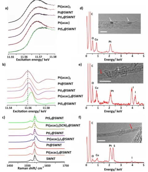
[image:4.595.50.286.555.652.2]In a representative example, an individual filled nanotube with a diameter of ca 1.52 nm, that corresponds to that of a (11,11) SWNT (figure 5a), is observed to contain a quasi-one-dimensional PtI2
crystal characterised by a close-packed cubic lattice (figure 5c). In the bulk, PtI2 crystals pack in the P2(1)/c group of symmetry with
each Pt six-coordinate and each I three-coordinate.33 Such an
arrangement of atoms gives rise to a monoclinic lattice with a unit cell 6.59 Å x 8.71 Å x 6.89 Å, which although could fit into the cavity of a SWNT, leads to a large void inside the SWNT, and so the packing of the PtI2 changes to better fit into the SWNT and minimise the
empty space. Therefore, the stoichiometry of Pt and I is maintained, but the arrangement of atoms changes as compared to that in bulk PtI2. Specifically, while the interatomic Pt-I distances remain the
same as in the bulk crystal and Pt is still six-coordinate, the iodine atoms change coordination numbers to range from 1 to 6, depending on their position within the new unit cell (SI section 4, figure S-12). This allows a more compact structure with a more suitable unit cell commensurate with the size of SWNT. AC-HRTEM imaging and TEM image simulation reveal a type of lattice that is closer to a cubic rather than monoclinic (figure 5b), with high-coordinated I-atoms in the middle of the structure and low-coordinated I-atoms located between in the space between Pt and SWNT wall, such that the overall ratio of Pt to I is 1 : 2, the same as in the bulk crystal.
Lattice measurements in experimental AC-HRTEM images showed regular spacings between atomic positions in the direction parallel to the nanotube of 0.39 nm, compared to a distance of 0.381 nm between I atoms in the asymmetric unit of bulk PtI2. Such a level of
distortion in inorganic structures is consistent with the literature and is a result of the confined lattice adapting to the nanotube channel in order to increase van der Waals interactions with the nanotube sidewalls.6, 14, 32 Similarly, there appears to be a slight increase in the
observed diameter of the SWNT due to an elliptical distortion of the nanotube channel to accommodate the PtI2 species (figure 5d and e)
which has also been reported previously for such systems.16
Computational modelling was utilised to generate a 3D representation of PtI2@SWNT (figure 5f) to enable comparison with
experimental AC-HRTEM images. AC-HRTEM images were then calculated by a TEM image multislice simulation package (QSTEM) using a model of a (11,11) SWNT filled with a structure derived crystal
Figure 4: a and b ) FD-XAS showing the Pt LIII edge of materials
formed in SWNTs, using molecular precursors containing suitable amounts of material for the formation of PtI2@SWNT (a) and
PtS2@SWNT (b), The raw data (black) has been overlaid on the
smoothed versions; EDX spectra recorded at 100 keV primary electron energy and integrated over a small bundle of nanotubes showing c), PtI2@SWNT; and d), PtS2@SWNT, both formed via the
thermal decomposition of molecular precursors containing the desired stoichiometric ratios of the two elements inside SWNTs. The spectra confirm the successful formation of the inorganic materials inside the nanotubes in each case (N.B. Cu peaks are due to the TEM specimen grid).
Figure 5: a) An AC-HRTEM micrograph showing a bundle of PtI2@SWNT in which the majority of the SWNTs are highly filled
with inorganic material, the scale bar is 5 nm; b) An extended portion of the crystal structure of PtI2 derived from the asymmetric
unit of bulk PtI2 with key atomic distances shown; the grey and
purple spheres represent platinum and iodine atoms respectively; c) an AC-HRTEM micrograph showing a small section of a 1.52 nm SWNT containing PtI2 material and the corresponding atomic
distances to the structure in b) are shown. A HR-TEM simulation (80 kV) showing a projection of how a portion of the derived PtI2
structure could fit inside an (11,11) SWNT, complimented by the cross-section of computational simulation to show its shape in the nanotube, the scale bar is 0.5 nm; d) an AC-HRTEM of the same section of nanotube with the material in a different orientation is shown, along with an AC-HRTEM simulation (80 kV) showing a projection of the model from (c) when rotated 90o parallel to the
nanotube axis, and a computational simulation of this model to show its shape in the nanotube, the scale bar is 0.5 nm; e) a simulation to show how the crystal fragment would appear when looking down the nanotube. The red and blue boxes represent the sections of the tube visible in figures c and d respectively; f) a geometry optimised model showing how the proposed PtI2 crystal
[image:5.595.44.283.62.353.2] [image:5.595.305.549.78.479.2]fragment. The simulated images (80 kV voltage, Scherzer conditions for under focus, spherical aberration parameter CS=10 µm) are in
good agreement with the experimentally obtained images (figure 5c, d, and e). The presence of terminal iodine atoms within the structure is supported by local probe, quantitative EDX analysis which reveals a Pt:I ratio of 1:2.11, see SI file section 5.
In bright-field AC-HRTEM images (figure 5) the observed contrast is determined by a complex mixture of dynamic effects depending on thickness and crystallinity of the structures as well as the actual focus conditions and the atomic number of the individual atoms, which makes the discrimination between different elements, particularly those similar in atomic number, complex. As a consequence, without quantitative image simulation, bright-field TEM is not a very efficient method for distinguishing between two heavy elements such as Pt (Z=78) and I (Z=53) present in our material. Therefore, it is important to confirm the identities of the atoms within the lattice using a complimentary technique, high angle annular dark-field aberration-corrected scanning transmission electron microscopy (HAADF-AC-STEM). With HAADF-AC-STEM the intensity of contrast is proportional to Zα, where α depends on the detector angle and is
typically 1.7-1.8 making it easier to distinguish between two heavy atoms within the same structure.34 Indeed, HAADF-AC-STEM images
of PtI2@SWNT clearly show a cubic lattice (figure 6a), similar to that
observed with AC-HRTEM and correlates well with the proposed model of encapsulated PtI2.
AC-HRTEM images of PtS2@SWNT material prepared in the
one-pot-one-reactant synthesis clearly show extended inorganic nanostructures within the channels of SWNTs (figure 7a). In contrast to the encapsulated PtI2@SWNT, only platinum atom columns can be
individually resolved by AC-HRTEM in this sample due to the significant difference between the atomic numbers of sulfur and platinum. The encapsulated material in PtS2@SWNT is characterised
by a hexagonal lattice analogous to that of bulk PtS2 (figure 7b). The
edge of the encapsulated PtS2 adopts a zigzag conformation, with
only sulfur atoms in contact with the nanotube sidewall (Figure 7c,d) and the Pt-Pt separations of the encapsulated PtS2 matching those in
the bulk PtS2. An HAADF-AC-STEM image of PtS2@SWNT (figure 7e)
clearly shows a tilted hexagonal lattice of Pt atoms matching that in AC-HRTEM images for this material (figure 7c). The Pt-Pt spacings appear to be in much closer agreement with bulk PtS2 with only a
small increase in the direction parallel to the principal SWNT axis. Although the nanotube sidewall cannot be observed in HAADF-STEM, in contrast to the images obtained using bright field AC-HRTEM, only three layers of platinum atoms are present in this sample suggesting that the host nanotube is narrower than in figure 7c (figure 7f). The structural assignment is supported by local probe, quantitative EDX analysis which reveals a Pt:S ratio of 1:1.93, see SI section 5.
Conclusions
Inorganic synthesis at the nanoscale is an important, but challenging task because of the need for simultaneous control of the dimensionality and stoichiometry of nanostructures. Carbon nanotubes, acting as nanocontainers effectively provide strict
Figure 6: a) HAADF-AC-STEM image showing a SWNT containing PtI2 in which the SWNT is highly filled with the inorganic
material, the scale bar is 1 nm; b)HAADF- AC-STEM micrograph showing a small section of a SWNT containing PtI2 material and
the corresponding atomic distances to the derived structure of PtI2. The material adopts a cubic configuration analogous to that
observed in the bright field images in figure 5, the scale bar is 0.5 nm.
Figure 7: a) An AC-HRTEM micrograph showing a bundle of nanotubes containing PtS2 material. The majority of SWNTs
appear to be highly filled, and a single standing tube is visible, the scale bar is 5 nm; b) a portion of the crystal structure of bulk PtS2, with key atomic distances shown; the grey and yellow
spheres represent platinum and sulfur atoms respectively; c) an AC-HRTEM micrograph showing a small section of a 1.32 nm SWNT containing PtS2 and Pt-Pt interatomic distances
corresponding to PtS2 structure tilted by 45o are shown, the scale
bar is 0.5 nm; a HR-TEM simulation (80 kV) showing how PtS2
could fit inside a SWNT, complimented by a computational simulation to show its morphology in the nanotube; d) a geometry-optimised model depicting the cross section of PtS2@SWNT; e) a HAADF-AC-STEM image showing what
appears to be a single strand of PtS2 in a SWNT, the material
adopts a hexagonal configuration analogous to that shown in c); however, there are only three layers of atoms present suggesting that the nanotube is narrower, the scale bar is 0.5 nm. Furthermore, a STEM simulation (200 kV) showing how PtS2
[image:6.595.311.550.66.318.2] [image:6.595.45.277.474.667.2]control of the size and shape of nanostructures, as we have demonstrated in this study by employing SWNTs as reaction vessels for the direct inorganic synthesis of a series of Pt compounds at the nanoscale. A detailed comparison of the stepwise and one-pot synthetic approaches clearly illustrates the advantages of the latter in terms of efficiency. However, the stepwise approach offers an excellent opportunity for studying the mechanisms of host-guest interactions between the SWNT and encapsulated compounds. We have shown that a combination of FD-XAS and Raman spectroscopy can probe both the inorganic compound and the nanotube properties, and shed light on the direction and magnitude of electron transfer between the nanotube and compound inside. For example, two structurally related Pt complexes Pt(acac)2I2 and Pt(acac)2(SCN)2
have shown opposing electronic interactions with SWNTs, withdrawing or donating electron density from/to the host-nanotube, which alters both the oxidation state of the Pt and the vibrational properties of the SWNT. However, neither one-pot nor stepwise approaches appeared to be able to provide sufficient control of the stoichiometry in the inorganic products formed inside the nanotube.
We found a solution to this problem by exploiting the diversity of the coordination chemistry of Pt complexes acting as precursors for the inorganic nanostructures. We expanded the coordination environment of the Pt-atom in the precursor complex by appending extra ligands bearing the necessary elements (I or S) in a correct and precise proportion to Pt, thus paving the way to stoichiometrically controlled synthesis inside nanotubes, as demonstrated by the synthesis of novel PtI2@SWNT and PtS2@SWNT nanostructures in
the new one-pot-one-reactant approach with the specifically designed multi-element containing precursors. The new strategy for inorganic synthesis at the nanoscale was shown to be versatile and universal, enabling the formation of previously inaccessible quasi-one-dimensional Pt-containing nanomaterials suitable for a variety of technological applications.35, 36 These range from
electronic devices where electronic doping of the nanotube is precisely modulated by electron transfer between the SWNT and encapsulated compound, to new catalytic platforms exploiting the unique chemical properties of platinum compounds, where the shape of the crystal and oxidation state of the metal are controlled by steric and electronic interactions with the host-nanotube.
Experimental
Materials
SWNTs (P2-SWNTs, arc discharge, Carbon Solutions, USA) were annealed at 600 oC for 15 min to open their termini and remove any
residual amorphous carbon from their internal cavities resulting in a 50% weight loss being observed. The platinum precursor, Pt(acac)2
was used as supplied (Sigma Aldrich). The substituted platinum precursors Pt(acac)2I229 and Pt(acac)2(SCN)230 were synthesised in
accordance with published procedures.
PtI2@SWNT
Pt(acac)2 (90 mg, 0.229 mmol) and freshly opened SWNTs (25 mg)
were sealed together under vacuum (10-5 bar) in a Pyrex ampoule
and heated at 150 oC for 3 days to ensure penetration of the SWNT
by the Pt(acac)2. The ampoule was cooled rapidly in ice-water and
repetitive washing with dichloromethane (4 x 25 mL) was performed, followed by filtration to remove any excess material from the
exterior of the SWNTs, forming Pt(acac)2@SWNT. Under an
atmosphere of argon, Pt(acac)2@SWNT (10 mg) was heated at 500 oC for 1 h and allowed to cool down slowly forming Pt@SWNT. This
sample was sealed in a Pyrex ampoule with an excess of I2 and heated
at 110 oC for 3 days to give PtI
2@SWNT.
Alternatively, Pt(acac)2I2 (10 mg 0.0192 mmol) was sealed in a Pyrex
ampoule under vacuum (10-5 bar) with freshly opened SWNTs (5 mg)
and heated for 3 days at 150 oC. The ampoule was cooled rapidly in
ice water and then heated under argon at 500 oC for 1 h to give
PtI2@SWNT
PtS2@SWNT
Argon was passed over PtI2@SWNT (5.7 mg) in a tube furnace for 1
h. The sample was then heated in the presence of a moderate H2S
gas flow (ca. 15mL/min) at 550 oC for 2 h. The sample was then
allowed to cool by 5 oC/min under argon.
Alternatively, Pt(acac)2(SCN)2 (10 mg, 0.0196 mmol) was sealed
under vacuum (10-5 bar) in a Pyrex ampoule with SWNTs (5 mg) and
heated at 130 oC for 3 days. After rapidly cooling in ampoule in ice
water, the sample was washed with chloroform (4 x 10 mL), then heated under argon at 500 oC for 1 h to give PtS2@SWNT.
Electron Microscopy
SWNTs filled with the encapsulated materials were dispersed in propan-2-ol using an ultrasonic bath and drop cast onto lacey carbon-coated copper TEM grids (Agar). HRTEM imaging was carried out on a JEOL 2100 FEG-TEM microscope operated at 200 kV. AC-HRTEM was performed at the University of Ulm on a Cs corrected FEI
Titan 80-300 TEM operated at 80 kV with information limit enhancement using reduced extraction voltage. HAADF-AC-STEM was performed at the University of Birmingham using a 200 kV JEOL 2100F microscope fitted with a CEOS probe corrector and a HAADF detector.
EDX Spectroscopy
Local EDX spectra were acquired for samples mounted on TEM grids using an Oxford Instruments INCA X-ray microanalysis system. The electron beam was condensed onto areas of specimens (bulk specimen or nanotube bundles) suspended over holes of the amorphous carbon film.
Raman Spectroscopy
Raman spectroscopy was performed using a HORIBA Jobin Yvon LabRAM HR spectrometer equipped with an automated xyz stage (Märzhäuser). Spectra were acquired using a 532 nm laser at 0.2mW power, in the range 50 to 4000 cm−1, with 5 seconds and 8
accumulations per spectral window, using a 50× objective and a 300 μm confocal pinhole. To simultaneously scan a range of Raman shifts, a 600 lines/mm rotatable diffraction grating along a path length of 800 mm was employed. Spectra were detected using a SYNAPSE CCD detector (1024 pixels) thermoelectrically cooled to −60 °C. Before the spectra collection, the instrument was calibrated using the Rayleigh line at 0 cm−1 and a standard Si (100) reference band at 520.7 cm−1.
HR-TEM image simulation was carried out using the multislice program QSTEM. QSTEM uses the Dirac-Fock scattering potential of Rez et al.37 A fixed number of 20 slices per nanotube were chosen
and images were calculated with a sampling of 0.05 nm per pixel. The aberration coefficients and defocus parameters df, CS, A1, and B2
were set according to the imaging conditions in the specific experiment. The convergence angle was fixed at 0.5 mrad. The effect of limited electron dose was emulated by applying noise to the calculated images using a custom-made Monte-Carlo program exploiting the Poisson statistics of electrons. Atomic models of SWNTs were built using a custom-made program taking into account different nanotube chiralities, if determinable in the experimental images. The structural models of the inorganic nanomaterials are based on scaled bulk structures and the complex models (PtX@SWNT, X = Pt, S) are rendered and iteratively fitted to the experimental results.
STEM image simulation was performed using both a kinetic approach (for speed) and frozen phonon multislice method to check for dynamical scattering effect which is found to be insignificant.38, 39 The
simulation was performed at 200 keV, with a Cs of 10 μm, convergence angle of 25 mrad, inner collection angles 60 mrad, outer collection angle of 160mrad, and a mechanical vibration factor of 0.1 Å.
Fluorescence-Detected X-ray Absorption Spectroscopy (FD-XAS)
All FD-XAS measurements were carried out on the XMaS beamline (BM28) at the ESRF. Samples were deposited onto carbon tape, which was then mounted onto a stainless steel sample holder. FD-XAS edge inflection points were obtained by fitting a smoothing spline to the measured spectrum, and taking the first derivative of the fitted spectrum.
Acknowledgements
C.T.S., T.W.C., G.A.R., A.B., M.W.F., and A.N.K. acknowledge support of the European Research Council (ERC), the Engineering and Physical Science Research Council (EPSRC), and the Nanoscale & Microscale Research Centre (NMRC) for access to instrumentation. J.B. and U.K. acknowledge support of the German Research Foundation (DFG) and the Ministry of Education and Research of the State of Baden-Württemberg within the SALVE project. Z.Y.L. and J.Y. acknowledge the support of EPSRC grants (EP/G070326/1 and EP/G070474/1). The AC-STEM instrument employed in this research was funded through the Birmingham Science City Project.
References
1. K. Yanagi, Y. Miyata and H. Kataura, Adv. Mater., 2006, 18, 437.
2. T. Takenobu, T. Takano, M. Shiraishi, Y. Murakami, M. Ata, H. Kataura, Y. Achiba and Y. Iwasa, Nat. Mater., 2003, 2, 683.
3. Y. Ren and G. Pastorin, Adv. Mater., 2008, 20, 2031. 4. N. A. Kiselev, A. S. Kumskov, V. G. Zhigalina, N. I. Verbitskiy,
L. V. Yashina, A. L. Chuvilin, A. L. Vasiliev, A. A. Eliseev and Iop, in 18th Microscopy of Semiconducting Materials
Conference, eds. T. Walther and J. L. Hutchison, 2013, vol.
471.
5. R. R. Meyer, J. Sloan, R. E. Dunin-Borkowski, A. I. Kirkland, M. C. Novotny, S. R. Bailey, J. L. Hutchison and M. L. H. Green, Science, 2000, 289, 1324.
6. J. Sloan, S. J. Grosvenor, S. Friedrichs, A. I. Kirkland, J. L. Hutchison and M. L. H. Green, Angew. Chem.-Int. Edit., 2002, 41, 1156.
7. M. Hulman, P. Costa, M. L. H. Green, S. Friedrichs and H. Kuzmany, in Electronic Properties of Synthetic Nanostructures, eds. H. Kuzmany, J. Fink, M. Mehring and
S. Roth, Amer Inst Physics, Melville, 2004, vol. 723, pp. 278. 8. E. Flahaut, J. Sloan, S. Friedrichs, A. I. Kirkland, K. S. Coleman, V. C. Williams, N. Hanson, J. L. Hutchison and M. L. H. Green, Chem. Mater., 2006, 18, 2059.
9. B. C. Satishkumar, A. Taubert and D. E. Luzzi, J. Nanosci.
Nanotechnol., 2003, 3, 159.
10. A. Chuvilin, E. Bichoutskaia, M. C. Gimenez-Lopez, T. W. Chamberlain, G. A. Rance, N. Kuganathan, J. Biskupek, U. Kaiser and A. N. Khlobystov, Nat. Mater., 2011, 10, 687. 11. T. W. Chamberlain, J. Biskupek, G. A. Rance, A. Chuvilin, T.
J. Alexander, E. Bichoutskaia, U. Kaiser and A. N. Khlobystov, ACS Nano, 2012, 6, 3943.
12. L. Shi, P. Rohringer, K. Suenaga, Y. Niimi, J. Kotakoski, J. C. Meyer, H. Peterlik, M. Wanko, S. Cahangirov, A. Rubio, Z. J. Lapin, L. Novotny, P. Ayala and T. Pichler, Nat. Mater., 2016, 15, 634.
13. A. K. Geim and I. V. Grigorieva, Nature, 2013, 499, 419. 14. C. G. Xu, J. Sloan, G. Brown, S. Bailey, V. C. Williams, S.
Friedrichs, K. S. Coleman, E. Flahaut, J. L. Hutchison, R. E. Dunin-Borkowski and M. L. H. Green, Chem. Commun., 2000, 2427.
15. J. Sloan, M. C. Novotny, S. R. Bailey, G. Brown, C. Xu, V. C. Williams, S. Friedrichs, E. Flahaut, R. L. Callender, A. P. E. York, K. S. Coleman, M. L. H. Green, R. E. Dunin-Borkowski and J. L. Hutchison, Chem. Phys. Lett., 2000, 329, 61. 16. E. Philp, J. Sloan, A. I. Kirkland, R. R. Meyer, S. Friedrichs, J.
L. Hutchison and M. L. H. Green, Nat. Mater., 2003, 2, 788. 17. L. V. Yashina, A. A. Eliseev, M. V. Kharlamova, A. A. Volykhov, A. V. Egorov, S. V. Savilov, A. V. Lukashin, R. Puttner and A. I. Belogorokhov, J. Phys. Chem. C, 2011, 115, 3578.
18. A. A. Eliseev, M. V. Chernysheva, N. I. Verbitskii, E. A. Kiseleva, A. V. Lukashin, Y. D. Tretyakov, N. A. Kiselev, O. M. Zhigalina, R. M. Zakalyukin, A. L. Vasiliev, A. V. Krestinin, J. L. Hutchison and B. Freitag, Chem. Mater., 2009, 21, 5001.
19. Z. Wang, H. Li, Z. Liu, Z. Shi, J. Lu, K. Suenaga, S.-K. Joung, T. Okazaki, Z. Gu, J. Zhou, Z. Gao, G. Li, S. Sanvito, E. Wang and S. Iijima, J. Am. Chem. Soc., 2010, 132, 13840.
20. Z. Wang, K. Zhao, H. Li, Z. Liu, Z. Shi, J. Lu, K. Suenaga, S.-K. Joung, T. Okazaki, Z. Jin, Z. Gu, Z. Gao and S. Iijima, J. Mater.
Chem., 2011, 21, 171.
21. A. Botos, J. Biskupek, T. W. Chamberlain, G. A. Rance, C. T. Stoppiello, J. Sloan, Z. Liu, K. Suenaga, U. Kaiser and A. N. Khlobystov, J. Am. Chem. Soc., 2016, 138, 8175.
22. Q. Fu, G. Weinberg and D. S. Su, New Carbon Mater., 2008,
23, 17.
23. F. Zhang, F. Jiao, X. L. Pan, K. Gao, J. P. Xiao, S. Zhang and X. H. Bao, ACS Catal., 2015, 5, 1381.
25. L. Grigorian, K. A. Williams, S. Fang, G. U. Sumanasekera, A. L. Loper, E. C. Dickey, S. J. Pennycook and P. C. Eklund, Phys.
Rev. Lett., 1998, 80, 5560.
26. S. Kiyohara, H. Takamatsu and K. Mori, Semicond. Sci.
Technol., 2002, 17, 1096.
27. V. Baranauskas, B. B. Li, A. Peterlevitz, M. C. Tosin and S. F. Durrant, J. Appl. Phys., 1999, 85, 7455.
28. J. X. Zhao and B. Q. Dai, Mater. Chem. Phys., 2004, 88, 244. 29. P. M. Cook, L. F. Dahl, D. Hopgood and R. A. Jenkins, J.
Chem. Soc., Dalton Trans., 1973, 294.
30. A. Grabowski and W. Preetz, Z. Anorg. Allg. Chem., 1987,
544, 95.
31. A. A. Eliseev, L. V. Yashina, N. I. Verbitskiy, M. M. Brzhezinskaya, M. V. Kharlamova, M. V. Chernysheva, A. V. Lukashin, N. A. Kiselev, A. S. Kumskov, B. Freitag, A. V. Generalov, A. S. Vinogradov, Y. V. Zubavichus, E. Kleimenov and M. Nachtegaal, Carbon, 2012, 50, 4021.
32. N. A. Kiselev, R. M. Zakalyukin, O. M. Zhigalina, N. Grobert, A. S. Kumskov, Y. V. Grigoriev, M. V. Chernysheva, A. A. Eliseev, A. V. Krestinin, Y. D. Tretyakov, B. Freitag and J. L. Hutchison, J. Microsc., 2008, 232, 335.
33. G. Thiele, W. Weigl and H. Wochner, Z. Anorg. Allg. Chem., 1986, 539, 141.
34. Z. W. Wang, Z. Y. Li, S. J. Park, A. Abdela, D. Tang and R. E. Palmer, Phys. Rev. B, 2011, 84, 073408.
35. X. Y. Chia, A. Adriano, P. Lazar, Z. Sofer, J. Luxa and M. Pumera, Adv. Funct. Mater., 2016, 26, 4306.
36. H. J. Yin, S. L. Zhao, K. Zhao, A. Muqsit, H. J. Tang, L. Chang, H. J. Zhao, Y. Gao and Z. Y. Tang, Nat. Commun., 2015, 6, 8. 37. D. Rez, P. Rez and I. Grant, Acta Crystallogr. Sect. A, 1994,
50, 481.
38. D. S. He, Z. Y. Li and J. Yuan, Micron, 2015, 74, 47. 39. R. Aveyard, R. Ferrando, R. L. Johnston and J. Yuan, Phys.