ISSN Print: 2331-4222
DOI: 10.4236/wjet.2018.64056 Nov. 21, 2018 839 World Journal of Engineering and Technology
Design and Assembly of an Improvised Logic
Gates Simulator
Ramil B. Arante
College of Industrial Technology and Teacher Education, Caraga State University, Cabadbaran City, Philippines
Abstract
This study aimed at designing and assembling an improvised Logic Gates Simulator that can be utilized as an instructional device in basic digital elec-tronics instruction at Caraga State University Cabadbaran Campus, Philip-pines. This instructional device is believed to enhance the teaching-learning process and would also help address the scarcity of instructional equipment in the school and in the country. Descriptive method of research was em-ployed to come up with the design of the simulator based on the course con-tent of basic digital electronics subject. Acceptability of the improvised simu-lator based on standards set in this study was gathered from the experts as respondents using a self-made questionnaire. The data were treated using av-erage weighted mean utilizing parametric scales with verbal descriptions. Findings revealed that the improvised logic gates simulator is highly accepta-ble in terms of its cost and availability of components, design and construction, operations, and troubleshooting features. It is concluded that the improvised logic gates simulator is at par in terms of standards on instructional devices based on the evaluation results of experts and is therefore recommended to be used in basic digital electronics instruction. The simulator is an innovative answer and an alternate solution to the scarcity of instructional materials and devices at Caraga State University Cabadbaran Campus.
Keywords
Acceptability, Assembly, Digital Electronics, Design, Enhance Learning Activities, Improvised, Logic Gates, Simulator
1. Introduction
Mindanao, Philippines is rich in natural resources yet its provinces are consi-dered among the poorest in the country. Strategic Development Framework for
How to cite this paper: Arante, R.B. (2018) Design and Assembly of an Impro-vised Logic Gates Simulator. World Journal of Engineering and Technology, 6, 839-853.
https://doi.org/10.4236/wjet.2018.64056
Received: August 23, 2018 Accepted: November 18, 2018 Published: November 21, 2018 Copyright © 2018 by author and Scientific Research Publishing Inc. This work is licensed under the Creative Commons Attribution International License (CC BY 4.0).
DOI: 10.4236/wjet.2018.64056 840 World Journal of Engineering and Technology 2010-2020 envisions for a “peaceful and socially inclusive Mindanao having a strong, sustainable, competitive, ICT-driven, agri-industrial and resource-based economy that is responsive to the local and global opportunities” [1]. To realize this vision, Mindanao must have a strong human capital who will help harness its natural resources and provide support for the development its economic frontier in agri-industry, tourism and mineral industry. Mindanao’s human re-source, then, must be capacitated and continuously upgraded, for its labor force to meet the demands in the market and take full advantage of the opportunities accorded by its anticipated growth. Caraga State University which is situated in Mindanao would like to answer the call of capacitating the human capital to meet the demands of the present times.
Camarao defined and enumerated the importance and need of technology education. He claimed that education is the most efficient system of equipping people with knowledge, skills and attitudes essential for effective membership in society. Technology education, as described by Camarao, deals with the devel-opment of technical skills, knowledge and attitudes needed to enter and/or progress in the world of work or prepare people for productive and meaningful citizenship. Technology education seeks to help people become technology lite-rate and equips them with basic skills, knowledge and understanding of the scope, materials, equipment, processes, products, problems and developments in the world of work. It seeks to prepare people for work, either as skilled workers, technician, technologist or technology teacher and specialist [2]. In addition, Gregorio [3] explained one of the criteria of good teaching and learning based on Dewey’s Educational Philosophy that teaching is better when it provides learning experiences that will insure understanding.
Seron in his study sought to produce an operational amplifier circuit trainer and evaluated its effectiveness as an instructional tool to explain common func-tions and basic op-amp applicafunc-tions. This study is more or less similar to the present study because both study wanted to produce an instructional device to improve learning [4]. Meanwhile, logic gate is defined as an electronic circuit that has one or more inputs and only one output. The output is a logical func-tion of the inputs and has voltages at either 0 or 1 level [5].
DOI: 10.4236/wjet.2018.64056 841 World Journal of Engineering and Technology expensive but equally effective instructional devices which may facilitate instruc-tion. This is the reason why the researcher intends to design and construct an improvised logic gates simulator as an aid for an effective basic digital electron-ics instruction. It is conceived that to design and construct this simulator as an actual training aid, it would partially solved the problem of inadequacy of in-structional equipment and devices in many technical/vocational schools all over the country most particularly in Caraga State University Cabadbaran Campus. In addition, this simulator is envisioned to speed up the students’ skills devel-opment and work performance.
2. The Problem
The purpose of this study is to design and assemble an instructional model, a logic gates simulator as an aid in basic digital electronics instruction at Caraga State University Cabadbaran Campus during the academic year 2017-2018.
Specifically, the study sought answers to the following questions: 1) How will the improvised logic gates simulator be constructed as to: a) planning and designing;
b) construction; and
c) testing and troubleshooting?
2) As perceived by experts/peers, how acceptable is the simulator in terms of: a) cost and availability of components;
b) design and construction; c) operations; and
d) troubleshooting features?
3. Methodology
This study utilized descriptive method of research. This method outlined the feasibility project, the preparations, construction, and testing until it was opera-tional. Descriptive research from its name alone tend to describe and interpret the conditions or relationships that exist, opinions that are held, process that are going on, effects that are evident, or trends that are developing [6].
3.1. Flow of the Study
1) The first activity was to gather ideas and concepts from the work of other researchers and authors on the different procedures used in the construction of an improvised logic gates simulator. It also covered the identification and pro-curement of supplies and materials needed, estimates and costing in the making of the simulator.
DOI: 10.4236/wjet.2018.64056 842 World Journal of Engineering and Technology
3.2. Respondents
The respondents of this study were the experts/peers which evaluated the accep-tability of the improvised logic gates simulator in terms of costs and availability of components, design and construction, operations, and troubleshooting fea-tures. The instructors in Caraga State University Cabadbaran Campus handling electronics subjects were selected as experts/peers. There were six (6) instructors in electronics and all of them were utilized as respondents in evaluating the ac-ceptability of the simulator. This process is somewhat similar to the study of Donkor [7] which assess the learners’ acceptance and satisfaction with the vid-eo-based instructional materials that he created and utilized in teaching.
3.3. Instruments
Evaluation Guide. This questionnaire was given to experts/peers in order to
evaluate the acceptability of the improvised logic gates simulator in terms of costs and availability of components, design and construction, operations, and troubleshooting features. The content of this questionnaire was actually several questions that would determine whether the newly constructed simulator was assembled with safety accessories that would protect the user from any harm. Another set of questions also were included which would determine if the com-ponents being used during the construction were locally available and less ex-pensive. Another also was questions designed to determine if the simulator were correctly designed and appropriately constructed as an instructional device. Several questions also were integrated designed to determine if the simulator is easy to operate and easy to troubleshoot.
3.4. Scoring Procedures
To quantify the response-category of the experts’ responses on the acceptability of the improvised logic gates simulator in terms of costs and availability of components, design and construction, operations, and troubleshooting features, weights were assigned as follows:
Weight Category Verbal Description
3 Highly Acceptable (HA) If the simulator achieved above 90 percent of the standards being set in the study
2 Acceptable (A) If the simulator achieved 75 - 89 percent of the standards being set in the study
1 Not Acceptable (NA) If the simulator achieved below 75 percent of the standards being set in the study
4. Results and Discussions
assem-DOI: 10.4236/wjet.2018.64056 843 World Journal of Engineering and Technology bling, testing, and troubleshooting.
4.1. Planning and Designing
This part presents the preparation and the process involved in designing the en-tire circuit of the improvised logic gates simulator. It includes the identification and acquisition of the supplies and materials as well as the different tools and equipment needed for the construction of the simulator as a pre-requisite prior to the actual assembly.
4.2. Circuit Designs
In this section, accurate planning and designing of the intended functions of the improvised logic gates simulator started. Some designing procedures used in this study followed the steps outlined in the book entitled, “Digital Design” under combinational logic which includes the following:
1) The problem is stated [8].
2) The number of available input variables and required output variables is determined [8].
3) The input and output variables are assigned with letter symbols [8].
4) The truth table that defines the required relationships between inputs and outputs is derived [8].
5) The simplified Boolean Expression for each output is obtained [8]. 6) The schematic diagram is drawn [8].
The circuit design follows the concept and general idea of combinational logic circuits in digital systems where the simulator as a combinational circuit consists of logic gates whose outputs at any time are determined from the present com-bination of inputs. The operation of the logic gates were explained by Brain in “How Stuff Works”. Brain likened the logic gate to an electronic gate which open and close automatically depending on the signal output given by the com-bination of two or more inputs [9]. The design comprises of input variables, log-ic gates, and output variables. Furthermore, the loglog-ic gates simulator is designed into 7 vital parts: the NOT, OR, AND gates simulator, the Regulated Power Supply section, Combinational Logic Gates Circuits implementor, Logic Probe section, Diode Tester section, Oscillator section and the last part is the Bread-board section. Designing the seven sections separately facilitates easy construc-tion and troubleshooting.
1) Power Supply Section. Figure 1 is the schematic design of the power supply section of the simulator. This section comprises of the AC/DC input (12 V), the rectification stage with four diodes connected as a bridge type rectifier, the fil-tering stage, and the voltage regulation stage which produces an output voltage of 5 volts.
DOI: 10.4236/wjet.2018.64056 844 World Journal of Engineering and Technology Figure 1. Schematic diagram of the power supply section of the simulator.
Figure 2. Schematic diagram of the oscillator section of the simulator.
called an “Astable Multivibrator”. This means that when running, each transis-tor switches on and off alternatively. When one switches on, it forces the other one off until one of the capacitors discharges. When discharged, the transistor that is off then turns on and forces the other one off. This occurs repeatedly, sometimes thousands of times per second. The speed that the switching occurs depends on the value of both the capacitors and the resistors in the circuit. If the capacitors are large, the frequency (number of switching per second) is slow. If the capacitors have a small capacitance, the frequency is high. If the capacitors have equal capacitance, the time that each of the transistors is on or off is equal. If the capacitors are not equal, one transistor may be on for a long period of time and off for a short period. The other transistor would then be off for the long pe-riod of time and on for a short pepe-riod. The output from an oscillator is some-times called a “clock” because the voltage pulses are often used to operate other circuits at a certain frequency (times per second). The output of the oscillator as a clock will be used in the enhanced laboratory activities.
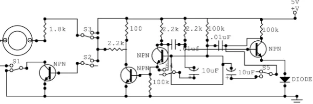
[image:6.595.213.534.192.299.2]DOI: 10.4236/wjet.2018.64056 845 World Journal of Engineering and Technology Figure 3. Schematic diagram of the AND, OR, NOT gate simulator section.
electronic switch in both forward and reverse bias. An LED also is used as an in-dicator of the output.
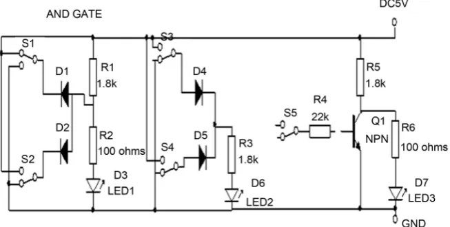
4) Combinational Logic Gates Circuit Section. Figure 4 is the schematic de-sign of the combinational logic circuit section of the simulator. This section pro-vides a set of logic gates that may be interconnected by the student to construct practical logic circuits. There are three black devices and the rows of small de-vices mounted down the middle of the board. The upper black pack contains six “NOT” gates (sometimes called inverters). The middle pack contains four “2 input OR gates”. The lower black pack contains four “2 input And gates”. The rows of small devices are the resistors necessary for the circuits to operate cor-rectly. Packs such as this are called “Integrated Circuits” or “IC’s” and in some cases may contain the miniature equivalent of hundreds of transistors, resistors and capacitors all interconnected to perform a special function. The four switches on the extreme right hand side permit the student to apply logic levels “1” or “0” (5 V or 0 V) to any pin on the logic board. Note that 5 V and 0 V power feeds to these switches are interconnected internally by the board.
5) Logic Probe Section. Below is Figure 5, the schematic diagram of the logic probe section of the simulator. This was adapted from the book of Latorilla [10] Electrical and Electronic Circuits for Engineers and Technicians. This section is an additional feature of the device. This part of the simulator provides the stu-dents alternative way in determining the logic state of a digital signal flowing in digital circuits. In many cases the common multimeter device does not suffice since in the digital world, there is what we call the undefined state or the “Don’t Care” where voltage is approximately in between 5 V and 0 V. This logic probe displays the three digital logic states: 1 (HIGH), 0 (LOW), and the undefined state (DON’T CARE) by lighting one of its three Light Emitting Diodes (LED). Logic 0 must not be higher than 0.7 V and is signaled by the LED D4. The logic 1 must not be less than 2.5 V and is signaled by D6. The logic levels between 0.7 V and 2.5 V is considered as the undefined state and is signaled by the LED D5.
DOI: 10.4236/wjet.2018.64056 846 World Journal of Engineering and Technology Figure 4. Schematic diagram of the combinational logic gates circuit section of the simu-lator.
Figure 5. Schematic diagram of the logic probe section of the simulator.
[image:8.595.215.535.574.702.2]DOI: 10.4236/wjet.2018.64056 847 World Journal of Engineering and Technology tester section of the simulator. This section provides solution to problems of de-termining the correct polarity of the diode when its markings are already erased. The color ring printed on one of its end usually marks the cathode terminal. But if this color is erased, the problem of determining its correct polarity can be solved using a multimeter. However, when one must test large number of un-marked diodes, multimeter becomes very uncomfortable to use. The best way to accomplish this kind of job is to use this section of the simulator. This circuit not only determines the polarity of the diode but also tests whether the diode is open or short circuited. The diode to be tested is connected to the terminals as shown
in Figure 6. When the LED lights, the diode are connected correctly and the
symbols or markings on the diode tester board show the correct polarity. To check whether the diode is shorted, reverse the diode and test it again. If the LED lights up again in this reverse position, then the diode has an internal short circuit. On the other hand when LED does not light up in both test directions, the diode is open [10].
7) The Breadboard Section. This section of the simulator allows the student to temporarily construct a given circuit without soldering it into a PCB. This is very useful especially in verifying the state of the different electronic components in-volved in building a particular circuit. You can easily detect and replace defective components temporarily constructed in the breadboard before the actual con-struction into a PCB (Printed Circuit Board).
5. Construction
The construction of the improvised logic gates simulator involved the following series of activities.
Layouting Printed Circuit Board (PCB) layouts were drawn and printed
ma-nually. These layouts were drawn based on the diagrams presented in Figures 1-6.
The copper side of the PCB is first covered by a masking tape. Then, a photo-copy of the original layout is pasted to the copper side of the PCB already cov-ered by a masking tape. Afterwards, the original layout was traced by a stylus pen and the unwanted parts were removed. The process lasted for about 15 mi-nutes considering the complexity of the circuit.
It is important to make the PCB layout as this is needed for the construction of the improvised logic gates simulator. The completed layout was then ready for the next stage called etching.
Etching Etching process was still similar to the traditional method where the
DOI: 10.4236/wjet.2018.64056 848 World Journal of Engineering and Technology
Drilling A process wherein holes are drilled into the etched PCB to allow the
electronic components and other parts to be mounted then soldered. A mini drill with drill bits of 1/32 inch or 1mm was used. This stage also included drill-ing of holes on the trainer’s chassis and panel board usdrill-ing portable electric drill with bits of 1/4, 1/2, & 3/4 inch respectively.
Mounting This was the stage when all parts and components were properly
placed in the drilled holes of the PCB prior to soldering. The order and correct parts placement was carefully followed. A list was prepared to properly identify the parts and parts placement guide from the source book was also used. The parts list and its specification are presented in Table 1.
Table 1 presents the list of electronic components used in the construction of the improvised logic gates simulator. The labels were designated as shown on various schematic diagrams of the different major sections of the simulator.
Soldering This stage included the proper soldering of all parts and
compo-nents into the PCB copper side. The process was done using a 30 watts soldering iron and a 60/40 soldering lead. Extra care was observed in order not to overheat any electronic components so as not to damage them specially the IC’s.
Assembling This is actually the final stage of the process of construction of
[image:10.595.163.535.409.742.2]the improvised logic gates simulator where all parts, electronic components were fitted into its respective places. All switches and dc power supply including the
Table 1. A List of electronic parts and its specification.
Component Label Specification
IC1 7805 Integrated Circuit Voltage Regulator IC2 7432 Integrated Circuit “2 Input OR Gate” IC3-IC4 7404 Integrated Circuit “NOT or INVERTERS”
IC5 7408 Integrated Circuit “2 Input AND Gate” IC6-IC7 7412 Integrated Circuit “2 Input NAND Gate”
R1-R59 1/4 Watt Carbon Resistor R60 5 Watts 4.7 Ω Resistor
C1 1000 uF/25 V Electrolytic Capacitor C2 & C3 100 uF/25 V Electrolytic Capacitor C4 4.7 uF/25 V Electrolytic Capacitor C6-C11 50 V Mylar Capacitor D1-D11 IN4001 Rectifier Diode D12-D14 Zener Diode 1 Watt 12 V D15-D36 Light Emitting Diode SW1-SW16 SPST Slide Switch
T1 12-0-12 750 Milliampere Transformer B1 Breadboard
DOI: 10.4236/wjet.2018.64056 849 World Journal of Engineering and Technology breadboard were mounted in place. This is also the stage where the entire parts of the trainer were properly labeled for proper identification of functions. Figure 7 is the actual appearance of the completed improvised logic gates simulator.
5.1. Testing and Trouble Shooting
The circuit of the improvised logic gates simulator was actually pre-tested to run using a computer-based program called “Electronic Workbench” before trans-ferring the layout into the PCB. Electronic Workbench is a Windows Software that would allow the circuit designs to be constructed and simulated in a com-puter to see how it responds. The logic gates simulator circuit design was tested and results were positive proving the veracity of the circuit designs.
[image:11.595.242.508.369.557.2]Next was testing all electronic components necessary for the construction. The circuit designs were actually constructed first in breadboards to physically ob-serve its response. A breadboard as shown in Figure 8, is a temporary PCB that allows construction of circuit designs without requiring the PCB layout and sol-dering for easy testing and assembling. This kind of test would individually test the electronic components as they were made to operate physically. Defective electronic parts were immediately replaced with good ones. Again this test yielded positive results as the circuit design functions as expected.
Figure 7. The improvised logic gates simulator.
[image:11.595.242.515.592.709.2]DOI: 10.4236/wjet.2018.64056 850 World Journal of Engineering and Technology It was only after the two pre-tests that the transferring of the circuit design into the PCB commenced in order to have 100 percent accuracy. Printed Circuit Board layouts were made and electronics parts were mounted and soldered in placed. After completing the process, the trainer was again tested for correct parts placement, cold solders and breaks.
Having finished with the assembly, the improvised logic gates simulator was made to run operational before enclosing in the chassis, testing and trouble-shooting of the finished device was done by checking its individual power and its respective output indicators. The improvised logic gates simulator was able to perform the seven logical operations. This final test proved that the simulator is functional and operational. Additional features like diode testers and logic probe also functions well thus making the performance of the newly developed simulator very versatile.
5.2. Acceptability of the Improvised Logic Gates Simulator
The data used to determine the acceptability of the logic gates simulator were collected and collated from the responses of experts/peers. These data were ana-lyzed and presented in Tables 2-5.
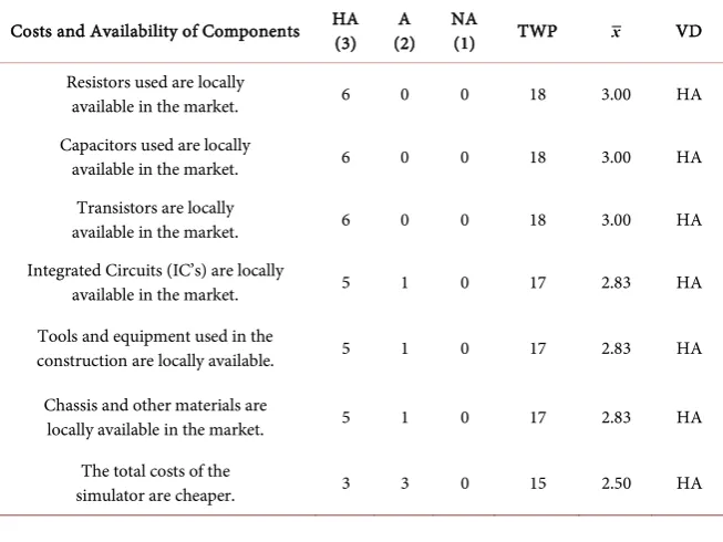
[image:12.595.210.537.492.737.2]Table 2 shows that the experts/peers generally regarded the costs and availa-bility of components of the simulator as Highly Acceptable, with weighted means of 3.00, 3.00, and 3.00, 2.83, 2.83, 2.83, 2.50 respectively. More so, it can be noted that none of the respondents had rated the improvised logic gates si-mulator as Not Acceptable. These findings further implied that in terms of costs, the simulator costs less than those instructional devices sold in the market with the same caliber. All the electronics components and the tools and equipment
Table 2. Acceptability of the improvised logic gates simulator in terms of costs and availability of components.
Costs and Availability of Components HA (3) (2) A NA (1) TWP x VD Resistors used are locally
available in the market. 6 0 0 18 3.00 HA Capacitors used are locally
available in the market. 6 0 0 18 3.00 HA Transistors are locally
available in the market. 6 0 0 18 3.00 HA Integrated Circuits (IC’s) are locally
available in the market. 5 1 0 17 2.83 HA Tools and equipment used in the
construction are locally available. 5 1 0 17 2.83 HA Chassis and other materials are
locally available in the market. 5 1 0 17 2.83 HA The total costs of the
DOI: 10.4236/wjet.2018.64056 851 World Journal of Engineering and Technology Table 3. Acceptability of the improvised logic gates simulator in terms of design and construction.
Design and Construction HA (3) (2) A NA (1) TWP x VD Safety features are integrated to
avoid electrical shock. 6 0 0 18 3.00 HA The design of the simulator is
compact and easy to handle. 4 2 0 16 2.67 HA Fuse holders are accessible and
fuses are easy to replace. 6 0 0 18 3.00 HA Voltage regulator acts like a safety
gadget for other components. 5 1 0 17 2.83 HA Vital components are accessible
for easy replacement. 5 1 0 17 2.83 HA Resistors are properly selected to operate
below their power stress levels. 6 0 0 18 3.00 HA Capacitors are properly selected to operate
below their working voltage. 6 0 0 18 3.00 HA Lower power transistors and Integrated
Circuits (IC’s) are reasonably placed away
from components that generate heat. 5 1 0 17 2.83 HA Terminals and switches are within easy
and comfortable reach of the students. 6 0 0 18 3.00 HA Parts of the simulator are properly labeled. 3 3 0 15 2.50 HA
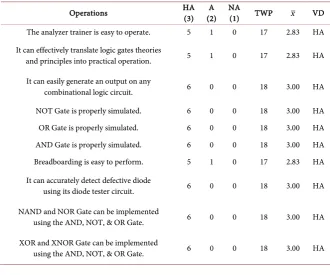
Table 4. Acceptability of the improvised logic gates simulator in terms of operations.
Operations HA (3) (2) A NA (1) TWP x VD The analyzer trainer is easy to operate. 5 1 0 17 2.83 HA It can effectively translate logic gates theories
and principles into practical operation. 5 1 0 17 2.83 HA It can easily generate an output on any
combinational logic circuit. 6 0 0 18 3.00 HA NOT Gate is properly simulated. 6 0 0 18 3.00 HA OR Gate is properly simulated. 6 0 0 18 3.00 HA AND Gate is properly simulated. 6 0 0 18 3.00 HA Breadboarding is easy to perform. 5 1 0 17 2.83 HA It can accurately detect defective diode
using its diode tester circuit. 6 0 0 18 3.00 HA NAND and NOR Gate can be implemented
using the AND, NOT, & OR Gate. 6 0 0 18 3.00 HA XOR and XNOR Gate can be implemented
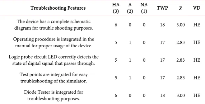
[image:13.595.206.537.460.735.2]DOI: 10.4236/wjet.2018.64056 852 World Journal of Engineering and Technology Table 5. Acceptability of the improvised logic gates simulator in terms of troubleshooting features.
Troubleshooting Features HA (3) (2) A NA (1) TWP x VD The device has a complete schematic
diagram for trouble shooting purposes. 6 0 0 18 3.00 HE Operating procedure is integrated in the
manual for proper usage of the device. 5 1 0 17 2.83 HE Logic probe circuit LED correctly detects the
state of digital signal that passes through. 5 1 0 17 2.83 HE Test points are integrated for easy
troubleshooting of the simulator. 5 1 0 17 2.83 HE Diode Tester is integrated for
troubleshooting purposes. 6 0 0 18 3.00 HE
used in the construction were locally available making it very convenient for fu-ture mass production and repairs.
Table 3 reveals the acceptability of the improvised logic gates simulator in terms of design and construction. The ten items were rated by the experts/peers as Highly Acceptable with weighted means of 3.00, 2.67, 3.00, 2.83, 2.83, 3.00, 3.00, 2.83, 3.00, and 2.50 respectively. The findings implied that the simulator is very safe to use. It was designed for easy access and user’s friendly allowing the users to easily manipulate and use this device hence making it a very convenient tool for learning. The table also revealed that none of the experts/peers rated the improvised logic gates simulator as Not Acceptable. This shows that the ex-perts/peers perceived that this newly developed instructional device would con-tribute much to the users understanding of logic operations based on the appro-priateness of the design and the good quality of construction.
Table 4 reflects the findings on the acceptability of the improvised logic gates simulator in terms of its operation. The experts/peers viewed the simulator as Highly Acceptable as revealed by the weighted means of 2.83, 2.83, 3.00, 3.00, 3.00, 3.00, 2.83, 3.00, 3.00, and 3.00 respectively. Not Acceptable have zero rat-ings. These results proved that the device can efficiently simulate the seven logi-cal operations plus it can also detect defective diodes using the diode tester cir-cuit. Users also can easily construct temporary circuits using the breadboard for testing and verification purposes before the actual construction of the designed circuit.
digi-DOI: 10.4236/wjet.2018.64056 853 World Journal of Engineering and Technology tal electronics instruction.
6. Conclusion
Based on the findings of the study, the improvised logic gates simulator is highly acceptable in terms of costs and availability of components, design and con-struction, operation, and troubleshooting functions as specified. It proved to be an effective tool in basic digital electronics instruction to perform and simulate logic gate operations. Furthermore, this presents an innovative approach in solving the problem of inadequacy of instructional materials and devices in state universities and colleges in the Philippines.
Conflicts of Interest
The author declares no conflicts of interest regarding the publication of this pa-per.
References
[1] NEDA (2010) Mindanao Strategic Development Framework.
http://www.neda.gov.ph/wp-content/uploads/2013/10/MSDF_finalforweb_2010-20
20.pdf
[2] Camarao, F.C. (1991) Technology Education in the Philippines. National Book Store Inc., Metro Manila.
[3] Gregorio, H.C. and Gregorio, C.M. (1979) Philosophy of Education in Philippine Setting. Garotech Publishing, Quezon City.
[4] Seron, S.L. (2002) Operational Amplifier Circuits Trainer: A Modular Device for Improving Electronics Technology Instruction at Southern Leyte State College of Science and Technology. Unpublished Master’s Thesis, Southern Leyte State Uni-versity (SLSU), Hinunangan.
[5] Greenfield, J.D. (1994) Practical Digital Design Using ICs. 3rd Edition, Prentice Hall Inc., Englewood Cliffs, NJ.
[6] Penaso, A.M., et. al. (2001) Methods of Research. Research and Development Unit. College of Education, Central Mindanao University, Musuan.
[7] Donkor, F. (2011) Assessment of Learner Acceptance and Satisfaction with Vid-eo-Based Instructional Materials for Teaching Practical Skills at a Distance. The In-ternational Review of Research in Open and Distance Learning, 12, 75-92.
https://doi.org/10.19173/irrodl.v12i5.953
[8] Mano, M.M. (1995) Digital Design. 2nd Edition, Prentice Hall Inc., Englewood Cliffs, NJ.
[9] Brain, M. (2017) How Electronic Gates Work.
https://electronics.howstuffworks.com/digital-electronics1.htm