General Purpose Wireless Communication System
Using Data Acquisition
Abdullah Eroglu, Bill Westrick
Indiana University-Purdue University Fort Wayne, Fort Wayne, USA Email: [email protected]
Received August 29, 2011; revised October 12, 2011; accepted November 10, 2011
ABSTRACT
A sensor-enabled and RFID-integrated, Wireless Data Acquisition System (WDAS) that has similar functionality as multiple input multiple output (MIMO) systems for health-care applications has been developed, simulated and imple-mented. The system can accept various measurements via sensors placed on patients or elders and transmit information wirelessly to base station at a remote location. A microcontroller is used to control and process the signals submitted from sensor-enabled RFID devices using sequential logic. Processed signals are then sent to single receiver and trans-mitter pair instead of conventional MIMO antenna systems. This reduces the cost significantly in comparison to existing systems. It has been shown that the data transmitted from measurement locations can be acquired at the base station located 20 mile away. Data acquisition system (DAQ) is used to determine the measured value, apply the required sta-tistics and display information to health-care professional at the base station. The system developed can be used for health-care applications including nursing homes in rural areas where access is difficult.
Keywords: WDAS; LabView; Multiple Input Multiple Output RFID; Sensor; Sequential Logic
1. Introduction
The recent developments in technology enabled profes-sionals to use real time wireless data acquisition (WDAS) technology in several areas including structural health monitoring and security systems, manufacturing plants, and health-care applications [1-3]. One of the common problems in WDAS is the distance between receiver and transmitter to have high accuracy and low cost [4,5]. If multiple measurements are required, this problem then gets worse and transmission problem and system imple-mentation difficulties arise. Multiple input and multiple output (MIMO) systems usually require several antennas at the transmitted and receiver locations. This adds an-other challenge to the system implementation by in-creasing the circuit complexity and its associated cost.
In this paper, sensor-enabled RFID device is used with a portable WDAS that can accept multiple measurements via sensors placed on patient or elder and transmit the measured signals wirelessly to base station which is lo-cated 20 mile away from the measurement point. System uses sequential logic with microcontroller and single RF transceiver system to reduce the cost and increase the communication distance. This eliminates the need to use conventional MIMO system where multiple antennas are needed at the input and output and hence reduces the cost significantly. Base station has RF receiver, receiver
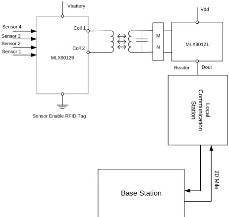
mi-crocontroller for post processing of the measured signals, and data acquisition system (DAS). DAS is equipped with a SC-2345 signal conditioner, 16 bit DAQ PAD 602E hardware, converter and interfacing circuits. DAQ system is used to determine the measured values, calcu-late of statistics to predict the behavior of the physical variables that are being measured, and display the results to health-care professionals. This system is general-pur- pose long-range low cost WADS that has same function-ality as MIMO and can be used in applications including health-care, and structural health monitoring. Implemen-tation of such as system with senor-enabled RFID device is illustrated in Figure 1.
2. Proposed Architecture of WDAS
The block diagram of the proposed MIMO WDAS is illustrated in Figure 1. System has seven different parts,
MLX90129 Sensor 4 Sensor 3 Sensor 2 Sensor 1 Vbattery Coil 1
Coil 2 MLX90121 M
N
Sensor Enable RFID Tag
Reader Vdd Dout Local Commu ni cation S tation Base Station 20 Mile
[image:2.595.309.533.85.218.2]captured, processed and displayed to the health-care pro-
Figure 1. Implementation of sensor-enabled WDAS system.
computer where all the measured values are processed, and displayed via LabView program. The custom de-signed conditioning circuits are used to convert the ana-log signal from the RFID device into digital signal that will be fed to microcontroller. It is also used to encode signal that will be transmitted with the proper format. The post-receiver conditioning circuit reverses the opera-tion of pre-transmission circuit and converts the trans-mitted signal back into an analog signal and normalizes it for SC-2345, signal conditioning unit. DAS unit, which has DAQ PAD 602E hardware with computer and Lab-View program processes the signals that will be dis-played to the health-care professional.
Signal transmission is accomplished using digital for-mat because digital signal transmission technology has high anti-jamming ability and reliability. RF transceiver pair ConnexLink (CL) 4790 [6] is used as a wireless transmission and reception module to increase the com-munication distance. Its frequency band changes between 902 to 928 MHz. It features Frequency Shift Keying (FSK) modulation and demodulation capability and it has transmission bit rates up to 115.2 kbps. Sensitivity of the module at full RF Data Rate is −99 dBm. The informa-tion regarding to RF transceiver’s data rate, power are provided in [6].
3. Implementaion and Simulation
System architecture that is proposed in Section 2 and shown in Figure 2 is implemented as a block diagram in Figure 3. It has mainly the transmitter section where all
the measurements have been performed and signal transmitted and receiver section where all signals are
Measurement Devices and Corresponding Circuits
3
Pre-Transmitter SignalConditioning Circuit Wireless Tranmitter
W ir e le s s ly T ran m it ted S igna l Wireless Receiver Post -Receiver Signal Conditioning Circuit SC-2345 DAQ Computer
1
2
4
RFID Signal7
6
5
[image:2.595.57.288.86.305.2]1 2 5 6 7 3 4
Figure 2. General block diagram of WDAS.
Measurement Devices and Cor responding
Ci rcuits
Pre- Tr ansmitter Signal Condi tioning Cir cuit
Measur ement Device Selecti on
Swi tch Signal Condi tioning A/D Conver ter MCU Memory RS 232 D/ R Line Dri ver MCU Control UART ACK Signal CL4790 Wir eless Transceiver CL4790 Wir eless Transceiver Wirelessl y Tr anmitted Signal
Post- Receiver Signal Conditi oning Circuit
RS 232 R/D Line Dr iver
D/A Conver ter UART MCU Memory Multipl exer LabVIEW User Interface on Computer SC-2345 DAQ RFID Signal
Figure 3. General block diagram of multiplexing circ t
ssional.
F channel is used to transmit multiple data si
ui using the ConnexLink 4790.
fe
Single R
[image:2.595.319.527.242.599.2]ssion circuit is controlled by microcon-tro
er, which converts th
m th
econd mi-cr
The transmi that are sent to the receiver MCU. These signals are 12-bit measurement signal from the transmitter and 3-bit select signal.
ller C8051F340 that selects the signal to be processed by digital to analog converter (DAC). The microcontrol-ler either cycles through each input channel, or through only the input channels selected by means of DIP switches. Once the conversion is completed, the digitized value is transferred to the microcontroller’s memory. The address of the multiplexer selecting the signal is ap-pended to the signal’s value. This combined data packet is then loaded into a UART. Hence, data packet is con-verted into a bit stream by this way.
The next stage is RS-232 line driv
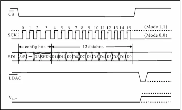
The 15-bit measurement signal from the transmitter is composed of 12-bit measurement signal from one of the measurement devices. 3-bit label designates the meas-urement device. 15-bit signal is first split into two signals, 3-bit label and 12-bit measurement signal. 12-bit signal is then sent via microcontroller’s UART to digital to analog converter. MCP 4822 is selected as digital to analog converter. Timing Diagram for the DAC conversion process is shown in Figure 4.
e TTL bit stream into higher voltage RS-232 bit stream in order to communicate with the CL4790. There are two input signals that are sent to the MCU. There is 12-bit digital measurement signal and 6-bit acknowledgement and select signal. 12-bit digital measurement signal comes from one of the five measurement devices that had been polled by the MCU and the analog to digital converter.
6-bit acknowledgement and select signal come fro
After D/A conversion, the signal is sent for signal conditioning. 3-bit label is sent into two different seg-ments of the program. It is first is sent to the SC-2345 signal conditioning box using 3-digital input ports for identification of the measurement signal. Acknowledge-ment signal is sent back to the transmitter to confirm the reception of the signal at the receiver end. 3-bit ac-knowledgement signal is then combined with the 3-bit select signal to form 6-bit signal that is sent to the UART at microcontroller and then to the RS-232 Line Driver. e receiver. 6-bit acknowledgement and select signal are
composed of 3-bit select signal and 3-bit acknowledge-ment signal. 12-bit measureacknowledge-ment signal is sent to the MCU’s universal asynchronous receiver/transmitter or UART. 6-bit acknowledgement signal is split between 3 separate 1-bit acknowledgement signals that are sent to an acknowledgement circuit and 3-bit select signal. 12- bit output of the UART and 3-bit select signal are then sent for sampling. The sampling code uses the MCU clock to choose a single 12-bit measurement signal and appends 3-bit label to create 15-bit output that is sent to the RS-232 Line Driver and then to the transmitter. The sampling code also creates 3-bit select signal to be sent to MUX for measurement device selection.
The receiver circuit is controlled by the s
The DAS receives two input signals: a 3-bit Label and a 5 V measurement signal. 3-bit signal is then sent into the digital input ports on the SC-2345 signal-condition- ing box. 5 V measurement signal is sent to SC-2345 us-ing 5 V analog input channel. The DAS software, Lab-View, uses label to identify the measurement device that the signal is coming from. The signal is then processed using the corresponding algorithm generated. The results are then displayed using LabView front panel.
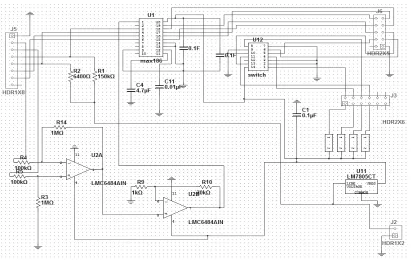
The transmitter and the receiver side of WDAS is simulated using National Instruments Multisim V11 cir-cuit simulator. The layout of the transmitter circir-cuit that is simulated illustrated in Figure 5.
[image:3.595.143.455.530.719.2]ocontroller C8051F340. There are two input signals
Figure 5. Layout of the simulated transmitter circuit for WDAS.
The RFID sensor circuit is also simulated for several different physical measurements. One of the input meas-urement devices is chosen to be a thermistor to measure temperature. The temperature that is measured by ther-mistor is calculated using a third order Steinhart-Hart equation as
1
ln
ln
3A B R
T C R (1) where T is temperature in Kelvin, R is the resistance in
ohms, A, B, C are Steinhart-Hart coefficients that depend
on the type of the semiconductor material. The equation given in (1) can be simplified by setting C = 0 and B = 1/b.
The equation then simplifies to
0 1
0e
T T
R R
(2) uation (2), R is defined as base resi
1
In Eq
defined as base temperature. Beta is calculated from 0 0 stance T is
0
0 0
R T T
(3) Taking the natural log of Equation (3) gives the fol-lo
ln R T T
wing equation
00 1 1
ln
R R
T T
tting
ln (4)
Plo ln
R versus
1T1T0
gives a linear re-s re-shown intance change in the termistor as depicted in Figure 7. The
sponse with adient a Figure 6. That can
be used to extract the measured temperature versus
resis-temperature measurement circuits that is used for simula-tion to measure temperature is given in Figure 8.
the gr
Gradient Beta
y = 3999.8x + 7.9278
0 1 2 3 4 5 6 7 8 9
‐0.0008 ‐0.0007 ‐0.0006 ‐0.0005 ‐0.0004 ‐0.0003 ‐0.0002 ‐0.0001 0
(1/T ‐1/T0)
ln
(R
[image:4.595.309.537.416.549.2])
Figure 6. Plot to determine β value for thermistor.
Temp
vs
Resistance
0 1000 2000 3000 4000 5000 6000 7000 8000
0 20 40 60 80 100 120
Temp ( 0 C)
res
is
tn
ac
e
(
Ω
)
Temp vs Resistance
(˚C)
[image:4.595.308.540.579.706.2]T1 HEL-700-U0B Ke y = T
-1
5.
0
R1 216O
J1
Space Key =
V1 15 V
R2 6400O
U1 the rmistor
1
2
RTD +
RTD -
THM +
THM
-to Multiplexer
Figure 8. Simulated temperature input measurement circui for WDAS.
urement circuit shown in Figure 8 is then
teg
on using sequential logic
t
The meas
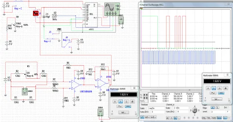
in rated with the input interfacing circuit that is con-nected to transmitter. The simulated circuit consisting of measurement circuit is given in Figure 9. The simulated
values closely matched with the measured values.
4. Measurement Results
WDAS for long-range applicati
is implemented and measured. The test has been per-formed in an outdoor environement. The transmitter and receiver have been separated up to 20 mile. The base station where receiver and DAS with all the hardware and software are located inside a closed structure where power was available. The transmitter is located outside and power is supplied using a portable power supply module.
It has been observed that the transmission and reception was good when there were no obstacles such as trees and buildings between the receiver and transmitter. Better communication was possible with the replacement of longer range receiver and transmitter antenna system. The measurement results at the receiver and transmitter sides are shown in Figures 10 and 11, respectively.
The trace that is colored in blue in Figures 9 and 10 is
the measurement signal. Figure 9 shows the transmitted
measurement signal whereas Figure 10 shows the
recon-structed signal at the base station. The signal that is col-ored in orange is the clock signal. As it is shown, WDAS was successfully implemented and used to transmit and receive the measurement signal. At the base station this acquired signal is then transmitted to DAS using LabView. The signal that is received is processed and the meas-urement values are displayed. This is illustrated in Figure 12.
5. Conclusions
[image:5.595.58.288.73.225.2]In this paper, design, simulation and implementation of a long-range portable MIMO wireless data acquisition system using sequential logic, which can accept several different measurement signals from sensor enabled RFID device for health-care applications is presented. It has been shown that the method that is used is superior to the existing systems in terms of cost and implementation. This type of MIMO system requires only one set of re-ceiver and transmitter antenna system using the proposed method. The DAS system equipped with LabView at the
Figure 9. Simulated input interfacing circuit for WDAS.
[image:5.595.56.536.464.715.2]
Clock Signal
[image:6.595.60.284.87.196.2]Measured Signal
Figure 10. Measurement result at the receiver for WDAS.
Clock Signal
[image:6.595.60.284.226.345.2]Measured Signal
Figure 11. Measurement result at the transmitter for WDAS.
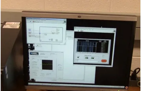
Figure 12. Labview display for WDAS.
base station facilitates the processing of the data that is acquired and displays the final measured value. It is also capable of doing statistical analysis and can be used as a warning system to raise the flag when such as condition occurs. The system that is developed can be utilized in several other applications in addition to health-care ap-plications such as structural health monitoring systems, and security systems.
REFERENCES
[1] K. Arshak, F. Adepoju and E. Jafer, “Simulation and Characterization of Wireless Data Acquisition RF Sys-tems for Medical Diagnostic Application,” Proceedings of IEEE Design and Diagnostics of Electronic Circuits and Systems (DDECS), Kraków, 11-13 April 2007, pp. 1-4. doi:10.1109/DDECS.2007.4295268
[2] K. Arshak and F. Adepoju, “Verification of Wireless Data Acquisition Radio Frequency System for Medical Te-lemetry Application,” International Spring Seminar on Electronics Technology, Cluj-Napoca, 9-13 May 2007, pp. 439-444.
B. Ko, Y. Shi, J. Basran s, “Data Acquisition System Using Six Degree-of-Freedom Inertia Sensor and Zigbee Wire-less Link for Fall Detection and Prevention,” Proceedings of IEEE Engineering in Medicine and Biology Society (EMBS), Vancouver, 20-24 August 2008, pp. 2353-2356. [4] L. X. Wang, S. Wei and L. Chao, “Implementation of
High Speed Real Time Data Acquisition and Transfer System,” Proceedings of IEEE Industrial Electronics and Applications Conference (ICIEA), Xi’an, 25-27 May 2009, pp. 382-386.
[5] Z. Yu, J. Wu, M. Xie and Y. Kong, “Implementation of Distributed High Precision Real-Time Data Acquisition System,” Proceedings of IEEE-NPSS Real Time Confer-ence, Beijing, 10-15 May 2009, pp. 446-449.
doi:10.1109/RTC.2009.5321600
[3] A. Dinh, D. Teng, L. Chen, S. and V. Del Bello-Has
[6] CL47 able
Re-placement System,” Datasheet.
[image:6.595.58.288.376.524.2]