Thesis by Wei-Qiao Deng
In Partial Fulfillment of the Requirements for the Degree of
Doctor of Philosophy in Chemistry
CALIFORNIA INSTITUTE OF TECHNOLOGY
Pasadena, California 2004
ii
2004
I wish to express my deep gratitude to my advisor, Professor William A. Goddard III, for his guidance in my PhD journey that consists of challenges and interests. His broad interest indeed showed me how many things a theorist can do. I appreciate what I have learned from him, not only the broad knowledge, sharp scientific instinct and creative ideas, but also the optimistic and confident personalities. I would also like to thank Professor Aron Kupperman, Professor Nathan S. Lewis, Professor Zheng-Gang Wang and Professor David G. Goodwin as my committee members.
I would like to thank Dr. Xin Xu, Dr. Richard P. Muller, Dr. Valeria Molinero and Sam Cheung for their collaboration in several topics and also thank all other people in the group who directly and indirectly contributed to my thesis. Especially, I would like to thank Darryl L. Willick and Shirley Wu for their warmhearted assistances.
I have spent six years at Caltech and I have had a great time here. My thanks go to all those who are responsible for this.
Funding for nano-electronics related topics came from MARCO at UCLA. I would like to thank all the collaborators at UCLA and Caltech in this project. Especially, I would like to thank Professor Fraser J. Stoddart, Professor James R. Heath and Dr. Amar Flood for their invaluable discussions.
Funding for fuel cell related topics came from General Motors. I would like to thank all the collaborators at GM fuel cell center who are pleasant to work with. Especially I would like to thank Dr. Gerald Voecks for his generous support and helpful discussions.
iv
We use multi-scale simulation strategy to understand, improve and rationally design novel materials with desired properties in molecular nanotechnology. The areas we have studied cover from molecular electronics, nano-structured materials to carbon nanotube technology.
In term of molecular and nano-electronics, first we used quantum mechanics to characterize the structure and current-voltage (I-V) performance of the Stoddart-Heath rotaxane-based programmable electronic switch. This methodology established a basis for iterative experimental-theoretical efforts to optimize systems for molecule-based electronics. We extended this switch principle and rationally designed an ultrafast molecular switch, proton-hopping molecular switch. Second we developed a kinetic model to study the hole mobility in organic semiconductor. After screening several designs, we presented a nano-bracelet as a competitive organic semiconductor.
We studied several topics related to the applications of nano-structured materials in fuel cell technology. Based on our simulation, we proposed a new kind of carbon-based materials for hydrogen storage. It can satisfy the target set up by the Department of Energy, USA. We develop a kinetic model to study the proton diffusion in proton exchange membrane of hydrogen fuel cell. We validated our proposed system, fluorinated imidazole impregnated nafion, as the candidate that can transfer proton above 100 0C at water – free media.
Acknowledgements...iii
Abstract ... iv
Table of Contents ... v
Chapter I: Introduction... 1
Section 1. Molecular and Nano-electronics ... 7
Chapter II: Mechanism of the Stoddart-Heath bistable rotaxane molecular switch ... 8
Chapter III: Ultrafast proton-hopping molecular switch ... 34
Chapter IV: Predictions of hole mobilities in oligoacene organic semiconductors from quantum mechanical calculations ... 52
Chapter V: The nano-bracelet, a new family of organic semiconductors... 83
Section 2: Nano-structured materials in Fuel Cell technology... 104
Chapter VI: Simulation of Li-doped pillared carbon based materials for reversible hydrogen storage... 105
Chapter VII: Fluorinated imidazoles as proton carriers for water-free fuel cell membranes ... 132
Section 3: Carbon Nanotube technology... 155
Chapter VIII: A two-stage mechanism of bimetallic catalyzed growth of single-wall carbon nanotubes ... 156
Appendix A: List of Publications ... 170
1
C h a p t e r I
INTRODUCTION
In 1959, the promise of nanotechnology was outlined by Nobel Prize laureate Richard Feynman in his famous talk, “There's Plenty of Room at the Bottom”. Since then, the concepts of molecular nanotechnology have extended to such as “molecular engineering” by Eric K. Drexler [1] and “molecular electronics” by Mark A. Ratner, [2] etc. Recently, the area of molecular nanotechnology has rapidly developed because enormous possibilities have opened to manipulate the molecular synthesis and movement. A lot of devices and applications have been demonstrated. [3] It is now not an impractical dream to fabricate molecular devices and molecular machines with atomic precision. In Figure 1, we show several highly active fields of molecular nanotechnology such as molecular electronics, carbon nanotube technology, organic electronics, self-assembly and its application, molecular machine and nano-structured materials.
Molecular electronics Carbon nanotube technology Nano Organic electronics
Self-assembly Nano-machine Nano-structured materials
Although there exists a continuing debate about the exact time frame to economically fabricate a wide range of structures with atomic precision, it is becoming acceptable that molecular nanotechnology will be the next industrial breakthrough. Most obviously a molecular manufacturing capability will be a prerequisite to the construction of molecular logic devices. It is necessary to be able to economically manufacture device at large scale with atomic precision. This capability will also require materials with expected properties that border on the limits imposed by natural law. A broad range of other nano-functionalized materials beside electronics materials will also benefit from a manufacturing process that offers atomic precision at low cost.
The promise of such remarkably high payoffs encourages people to seek the solutions, how such a system will work and how we can build such a system. Fortunately, with nowadays dramatic developing of computational technology at both hardware (computation speed) and software (parallel computation), our current understanding of chemistry and physics should be sufficient to simulate such nano systems that involves millions of atoms. It is here that the value of computational nanotechnology can be most clearly seen. We can simulate and validate thousands of designs in days even without doing any expensive experiments that may take years. With this computational nanotechnology, it becomes possible to rationally design systems at atomic precision.
Now, the challenge of computational nanotechnology is how to model a real nano system at atomistic scale and predict accurately the expected properties. To meet the challenge above, we will use the following computation aided design methodology. [4]
Figure 2 shows an overview of our computation aided design methodology. We propose three stages for designing in molecular nanotechnology.
3
This may involve chemical properties of single molecules, or may involve interaction between molecules.
Å nm micron mm cm meters
time distance hours minutes seconds microsec nanosec picosec femtosec MESO Continuum (FEM) QM MD Design process stage 1
Target properties at the macroscale determine the desired behavior at smaller scales
Design process stage 2
High quality multi-scale modeling of promising materials for accurate predictions of materials properties
Design process stage 3
Optimize designed materials by changing chemical components or nano-structures
Figure 2. The multi-scale simulation strategy and design processing
Stage Two, bottom-up stage: We will seek to understand macroscopic behaviors starting from the quantum mechanics level up to the continuum level. Initially, we will investigate critical system components by using ab initio quantum mechanics (QM) simulations to examine one or one part of one molecule at a time. These small-scale simulations will give us detailed and accurate pictures of key properties without incurring enormous computational cost. We will then use data from first principle simulations to build an accurate scale model without empirical parameters. Throughout the multi-scale modeling process, we will also use results of larger multi-scale simulations as input parameters for smaller scale simulations that more accurately reflect the conditions under which molecules operate. The data from improved smaller scale simulations will then be used to build better larger scale models. In this manner, we iterate between different scales to improve the accuracy of our models.
molecular layer alignment, electrode connection, etc. We will cooperate with the experimental side to gain quick feedback to re-design.
III. Proton hopping switch
VI. Carbon based hydrogen storage
V. Nano-bracelet
VII. Fluorinated Imidazole impregnated nafion for proton exchange membrane II. Mechanism of rotaxane switch
S O S S S
S S
O O
O O S
N
N N
N
+ +
+ +
N
Au Au
S H3C
S O S S S
S S
O O
O O S
N
N N
N
+ +
+ +
N
Au Au
S H3C
Section 1. Molecular and nano-electronics
Section 2. Nano-structured materials in fuel cell
Section 3. Carbon nanotube technology
VIII. Carbon nanotube growth
Figure 3. Introduction of three areas in the thesis.
Figure 3 summaries those novel designs in this thesis which we classified into three areas. They are organized as below:
5
In Chapter II, we used green functional theory combined with quantum mechanics to study rotaxane molecular switch and rationalized its switching mechanism. We found that the change in the delocalization of the MOs affected by the ring movement plays a key role in the switching mechanism. Using this mechanism we can now estimate how changes in the chemical components will change switch performance, providing a design principle for optimization.
In Chapter III, based on the principle of the configuration bistable structure switch, we presented a new design, ultrafast proton-hopping molecular switch, which is 106 faster than the current molecular switch. This switch may satisfy the goal of the next generation electronic device being searched by information industry.
In Chapter IV, we described the development of an incoherent kinetic model based on first principle calculation results to predict the hole mobilities of organic semiconductors. We calculated a hole mobility of 6.5 cm2/Vs for pentacene crystals at 300K. This can be compared to recent experimental results of 5 cm2/Vs, suggesting that current materials are approaching the maximum for the 3D crystal. Our model might be useful to screen new materials to have a higher hole mobility.
In Chapter V, by using the developed incoherent kinetic model, we screened various designs and presented a novel material, nano-bracelet, which may have an ultra-high hole mobility, 10-600 times faster than the current ones.
Section 2 describes several novel materials designed for hydrogen proton exchange membrane fuel cell technology. Those designs are presented in Chapter VI and VII, respectively.
In Chapter VII, we discussed how we design a novel water-free proton exchange membrane that can work above 100 0C (Figure 3). Our simulation showed that fluorinated imidazole impregnated nafion has comparable proton conductivity to the unfluorinated system, however it is chemically more stable and does not poison the electrodes.
Section 3 describes the research on one of the bottleneck problems in carbon nanotube technology, i.e., how to grow carbon nanotubes efficiently. In Chapter VIII, we proposed a two-stage mechanism for bimetal catalyzed carbon nanotube growth to explain why bimetal catalyzed growth can be 100 times more efficient than monometal catalyzed growth. Based on this two-stage mechanism, we screened a number of other metals (Cr, Fe, Mo, Rh, Pd) and suggested that Mo+Ni should be the best bimetallic catalyst from combining these elements (better than Ni+Co).
Reference
[1] Drexler, K. E. (1981) “Molecular engineering: An approach to the development of general capabilities for molecular manipulation.” Proc. Natl. Acad. Sci. U.S.A. 78:5275-5278, 1981.
[2] Aviram A. and Ratner M. A. “Molecular rectifiers” Chem. Phys. Lett. 29: 277-283, 1974.
7
Section 1: Molecular and Nano-electronics
Chapter II: Mechanism of the Stoddart-Heath bistable rotaxane molecular switch
Abstract ...8
Content ...9
Reference...12
Figures ...14
Support Information...17
Chapter III: Ultrafast proton-hopping molecular switch Abstract ...34
Content ...35
Reference...39
Figures ...40
Support Information...44
Chapter IV: Predictions of Hole Mobilities in Oligoacene Organic Semiconductors from Quantum Mechanical Calculations Abstract ...52
Introduction ...53
Theoretical Methodology...53
Results and Discussion ...59
Reference...65
Figures and tables...68
Chapter V: The nano-bracelet, a new family of organic semiconductors Abstract ...83
Content ...84
Reference...88
Figures ...90
C h a p t e r I I
MECHANISM OF THE STODDART-HEATH BISTABLE ROTAXANE MOLECULAR SWITCH *
Abstract
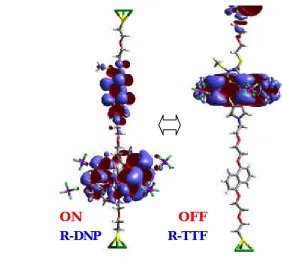
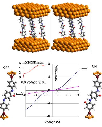
[image:13.612.145.427.391.659.2]We use quantum mechanics to characterize the structure and current-voltage (I-V) performance of the Stoddart-Heath rotaxane-based programmable electronic switch. We find that the current when the ring is on the DNP is 37~58 times the current when the ring is on the TTF, in agreement with experiment (ratio of 10 to 100). The basis is now established for iterative experimental-theoretical efforts to optimize systems for molecule based electronics which we illustrate by predicting the effect of adding a group such as CN group to the rotaxane.
Figure for Table of Contents (LUMOs for rotaxane molecule).
ON OFF
9
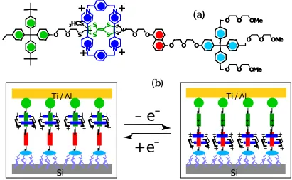
Molecular scale electronics is developing rapidly[1] because of advances in the synthesis of suitably tailored organic structures, bringing us closer to the ultimate miniaturization of nano-electronic devices.[2-3] A recent success by the Stoddart and Heath groups utilized rotaxanes, which have a ring component encircling the dumbbell-shaped component (Scheme 1), function as a programmable electronic switch.[4-9] The ring is a cyclobis(paraquat-p-phenylene) tetracationic macrocycle (CBPQT4+). The dumbbell is comprised of a tetrathiafulvalene (TTF) and a 1,5-dioxynaphthalene (DNP). Consequently, the ring can localize at either TTF site or DNP site along the dumbbell. The experiments showed conclusive evidence of two distinct states (one with a resistance 10 – 100 times that of the other) and that the system could be switched from one state to the other by applying two different sharp address voltages. Switching the device to an ON state is observed at the net oxidizing voltage +2 V, whereas, switching to an OFF occurs at –2V, or net reducing voltages. It is assumed that the switching behavior arises from the difference in conductivity between the two states. However, the atomistic-level mechanism of the conductivity switching is still unknown.
In order to provide the molecular level understanding necessary to design and optimize such nanoelectronic devices, we initiated theoretical studies on the mechanism of conduction for the bistable [2] rotaxane shown in scheme 1. This structure is based on a known compound [8] and for simplicity the stoppers at each end have been removed. The detailed simulation procedures are in Supportive Information (SI).
Scheme 1. The structure of the Au3-rotaxane-Au3 switch used in the simulation. Each
Au electrode includes three Au atoms.
S S
S S
N H3CS
S O S
O O
O O S
N N
N N+
+ + + Au Au S S S S N H3CS
S O S
O O
O O S
N N
N N+
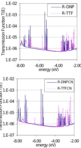
The calculation of electric conductivity at atomic level has been well established.[10-14] The I-V curves that were calculated by a combination of quantum mechanics [15-19] and green’s function theory [12-14] for the two states of the rotaxane are shown in Figure 1. Current flow through the state with the ring on DNP group (R-DNP) increase almost linearly to 1.5 nA from 0 to 0.25 V bias and reach its maximum 1.8nA after 0.3V. However, current through the state with the ring molecule on TTF group (R-TTF) increases only to 0.05 nA at range from 0 to 0.5 V shown in the Figure 1b. The calculation results show large different conductivities between the R-DNP and R-TTF states. For applied bias from 0.01V to 0.2V, the calculated On/Off ratio increases from 37 to 58 and decreases to 39 from 0.2V to 0.5 V applied bias. This On/Off ratio is comparable to experimental values [7] of 10-100. This suggests that the simulation has captured the essence of the experimental system. In particular, we find that the switch is OFF when the ring is on the TTF group (R-TTF) and ON when the ring is on the DNP group (R-DNP). Exactly this same assignment was previously proposed. [4,8]
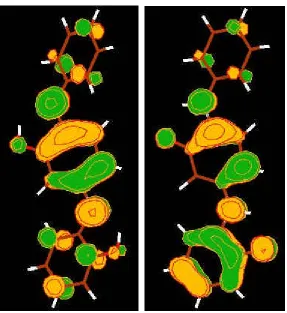
Next we examine the orbital basis for the switching behavior. The frontier MOs including highest occupied molecular orbital (HOMO), lowest occupied MO (LUMO), and nearby orbitals are shown in Table 1. Figure 1 shows the shapes of the HOMO and LUMO of DNP and TTF state respectively. More MOs can be found in SI. These MOs contain contributions from four groups of atoms: Au electrode atoms at each end, the TTF group, the DNP group, and the ring group: We find two states with distinct I/V differences
· R-DNP State (ON): The HOMO is delocalized over the TTF and ring groups. The LUMO and LUMO +1 (0.1 eV above the LUMO) is delocalized over the TTF and ring-DNP groups. HOMO-1 is localized near the upper Au electrode.
· R-TTF State (OFF): HOMO-2 is localized at DNP; LUMO and LUMO+1 is localized at the TTF. HOMO-1 and HOMO are mostly localized at the electrodes.
11
in the transmission function (except for the MOs localized on Au, which do not contribute to conductivity). For the R-DNP/ON state, HOMO, LUMO and LUMO+1 correspond to the three peaks in Figure 3 where HOMO contributes the highest peak (blue) because it is the most delocalized MO. For the R-TTF/OFF state, the HOMO-2, LUMO and LUMO+1 lead to three peaks (pink). These MOs are localized leading to transmission peaks 10 to 1000 times smaller than the peaks of the ON state. Thus, we conclude that the characteristics of MOs around the Fermi energy determine the electrical conductivities of Au-rotaxane-Au system.
With a plausible mechanism for understanding the switch in the rotaxane system, we can now use this mechanism to design improved devices. For example chemical groups could be attached to the rotaxane molecule so as to shift the frontier orbitals to make them more localized for the OFF state and/or more delocalized for the ON state. Therefore, to optimize the rotaxane switch we are considering changes like those in scheme 2, where each component of the switch can be functionalized separately. Which group best optimizes the switch depends upon which frontier orbital is tuned. To illustrate the procedure, we added a CN group, an electron acceptor on the DNP site to shift the characteristic of that orbital and change the distribution of the frontier orbitals. The red curve in Figure 3 shows the transmission with CN modification. The CN addition makes LUMO+1 more localized leading to a smaller transmission. This suggests that we should add the CN instead to the TTF region.
ACKNOWLEDGMENT We thank Fraser Stoddart and James Heath for helpful discussions and thank Xin Xu and Amar Flood for helpful suggestions. We thank Supriyo Datta and his group who provided details of their Huckel-IV 2.0 program. This research was supported by NSF-NIRT.
Reference
1. Tseng, G.Y.; Ellenbogen, J.C.; Science 2001 294, 1293.
2. Feynmann, R. P. In Miniaturization; Gilbert, H. D., Ed.; Reinhold: New York, 1961; p 282.
3. Aviram, A.; Ratner, M. A. Chem. Phys. Lett. 1974, 29, 277.
4. Collier C.P.; Mattersteig G.; Wong E.W.; Luo Y.; Beverly K.; Sampaio J.; Raymo F.M.; Stoddart J.F.; Heath J.R.; Science 2000, 289, 1172.
5. Wong E.W.; Collier C.P.; Behloradsky M.; Raymo F.M.; Stoddart J.F.; Heath J.R.; J. Am. Chem. Soc. 2000, 122, 5831.
6. Collier C.P.; Wong E.W.; Belohradsky M.; Raymo F.M.; Stoddart J.F.; Kuekes P.J.; Williams R.S.; Heath J.R., Science 1999, 285, 391.
7. Collier C.P.; Jeppesen J.O.; Luo Y.; Perkins J.; Wong E.W.; Heath J.R.; Stoddart J.F.; J. Am. Chem. Soc. 2001, 123, 12632.
8. Luo Y., Collier C. P., Jeppesen, J. O., Nielsen K. A., Delonno, E. and et. al Chemphyschem 2002, 3, 519
9. Pease, A. R. ; Jeppesen, J. O., Stoddart, J. F., Luo, Y., Collier C. P. and Heath, J. R. Acc. Chem. Res. 2001, 34, 433
13
11. Datta, S. Electronic Transport in Mesoscopic Physics; Oxford University Press: Oxford, 1997.
12. Yaliraki S.N.; Roitberg A.E.; Gonzalez C.; Mujica V.; Ratner M.A. J. Chem. Phys 1999, 111, 6997
13. Xue, Y.Q.; Datta S.; Ratner, M.A. J. Chem. Phys. 2001, 115, 4292
14. Seminario, J. M.; Zacarias, A.G.; Derosa, P.A. J. Phys. Chem. A 2001, 105, 791. 15. Mayo, S. L.; Olafson, B.D.; Goddard, W.A. J. Chem. Phys. 1990, 94, 8897 16. Mopac2000 package. Schrodinger Inc.
17. Hay, P. J. and Wadt, W.R. J. Chem. Phys. 1985, 82, 299. 18. Jaguar 4.0 from Schrodinger Inc, Portland Oregon
19. Papaconstantopoulos D.A. Handbook of the band structure of Elemental Solids; Plenum Press: New York, 1986.
-2.0 -1.5 -1.0 -0.5 0.0 0.5 1.0 1.5 2.0
-0.5 -0.3 -0.1 0.1 0.3 0.5
applied bias (V)
Curren
t (nA)
R-DNP R-TTF R-DNPCN R-TTFCN
(a) R-DNP
R-DNPCN R-TTF, R-TTFCN
-0.06 -0.04 -0.02 0.00 0.02 0.04 0.06
-0.5 0.0 0.5
applied bias (V)
Curren
t (nA)
(b) R-TTF
R-TTFCN
R-DNP/R-TTF
30 35 40 45 50 55 60
-0.5 0.0 0.5
Applied bias (V)
On/Off Ratio
[image:19.612.161.457.81.340.2](c)
15
ON OFF
LUMO
HOMO HOMO LUMO
R-DNP R-TTF
Figure 2. MOs of Au-rotaxane-Au switch. Green atoms are Au, Yellow is S, grey is C, red is oxygen and white is hydrogen. The ring is CBPQT4+, with 4 PF6- units around. The TTF
and DNP units are located at the top and bottom halves of the dumbbell, respectively. The total is 186 atoms.
Scheme 2 The strategy of the modifications for the rotaxane switch
N N
S S
S S
Connection between
molecule tail and electrode
N N N N
R
O
O
O
O R O
O O
O
S S
S S R
R = CN, OH
O
-5.8 -5.7 -5.6 -5.5 -5.4 -5.3 -5.2 -5.1 -5.0
1.00E-07 1.00E-06 1.00E-05 1.00E-04 1.00E-03 1.00E-02
Transmission Fuction T(E)
Energ
y (
eV)
R-DNP R-TTF R-DNPCN
R-DNP HOMO -5.38eV R-DNP LUMO -5.22eV R-DNP
LUMO+1 -5.15eV
LUMO: -5.38eV
LUMO+1: -5.23eV
R-TTF HOMO-2 -5.67eV
R-DNPCN HOMO -5.49eV R-DNPCN LUMO -5.31eV R-DNPCN
LUMO+1 -5.24eV
10-6
10-7 10-5 10-4 10-3 10-2
Fermi
[image:21.612.113.491.81.400.2]R-TTF R-TTF
17
Support information:
Mechanism of the Stoddart-Heath bistable rotaxane molecular switch Abstract
The supporting information is organized as follows:
Section S1 describes the real device and our strategy to make a minimum structure device for quantum mechanics and device simulations.
Section S2 describes the Green’s Function method and procedures we use to calculate the electronic properties of the device structure described in section 1.
Section S3 shows additional detailed results from the calculations. Section S1 Device structures and our approximation
OMe N N N N
+
+
+
+
N OMeO O S S S
S S
O O
O O O
O O OMe
O OMe O
O O
3HCS
OMe
O O S S S
S S
O O
O O O
O O OMe
O OMe O
O O OMe
N N N N
+
+
+
+
N OMe N N N N+
+
+
+
N 3HCS(a)
OMe N N N N+
+
+
+
N OMe N N N N+
+
+
+
N OMeO O S S S
S S
O O
O O O
O O OMe
O OMe O
O O
3HCS
OMe
O O S S S
S S
O O
O O O
O O OMe
O OMe O
O O OMe
N N N N
+
+
+
+
N OMe N N N N+
+
+
+
N 3HCS(a)
Si SiTi / Al Ti / Al
+ + + ++ ++ ++ + + + + + + + + + + + + + + + + + + + + + + + + + + + + + + +
– e
–
+ e
–
[image:22.612.105.516.354.607.2](b)
Figure S1. The scheme of Heath-Stoddart rotaxane switch
left green; stopper to keep ring from coming off the backbone, TTF group green,
DNP group red, and right blue: stopper.
The ring component can be caused to shift between the TTF and DNP group but cannot move off the dumbbell because of the left and right stoppers. Figure S1b shows the device structure, with the four components shown as colored boxes. The rotaxane was deposited on the poly-silicon surface and is expected to form a self-assembled monolayer. The second electrode, Ti/Al was deposited on the top of the monolayer.
We simplified the system as shown in Figure S2 to make the DFT calculations practical, while maintaining the essence of the rotaxane switch. From original molecule (a), we cut off the right and left stoppers and neutralize the molecule with hydrogen atoms. Then we used the Dreiding force field [15] to optimize the geometry for three structures:
ring over the TTF, ring over the DNP, and
ring over the linker in between
In all cases the four PF6- counterions are included. These structures were then
reoptimized using AM1 [16] quantum mechanics, leading to the result that the ring-linker structure is higher than the other two. Next we deleted the hydrogen atom at the thiol and bond the thiol to a gold trimer at each end of the rotaxane. This Au3 was included to
19
carried out DFT calculations (B3LYP) with the 6-31G basis on each atom except the Au atoms, where we used the Hay-Wadt core-valence effective core potential [12] (LACVP with 11 electrons per Au). We solved for the ground state Hamiltonian and orbitals for each state.[18]
To calculate the electrical conductivity, we used the Green’s function formalism of Ratner and others [12-14], assuming that the coupling between the backbone of the rotaxane and the electrodes does not change as the ring moves. A DFT calculation at the B3LYP/LACVP level was performed at single point calculation to obtain the Fock Hamiltonian and Overlap matrices. These Fock and Overlap matrices were then factored into electrode (Au3) and molecule parts. In these calculations we choose the Fermi energy
as –5.31eV, just as for bulk Au metal.
OMe
HS O S S S S S O O N
O O SH
N N N N
+
+
+
+
O O S S S
S S
O O
O O O
O O OMe
O OMe O
O O
3HCS
3HCS
S O S S S
S S
O O
O O S
N N N N
+
+
+
+
N Au Au S H3CS O S S S
S S
O O
O O S
N N N N
+
+
+
+
N Au Au S H3COMe
HS O S S S S S O O N
O O SH
N N N N
+
+
+
+
O O S S S
S S
O O
O O O
O O OMe
O OMe O
O O OMe
N N N N
+
+
+
+
N OMe N N N N+
+
+
+
N 3HCS 3HCSS O S S S
S S
O O
O O S
N N N N
+
+
+
+
N Au Au S H3CS O S S S
S S
O O
O O S
N N N N
+
+
+
+
N Au Au S H3C(a)
(b)
(c)
OMe
HS O S S S S S O O N
O O SH
N N N N
+
+
+
+
O O S S S
S S
O O
O O O
O O OMe
O OMe O
O O
3HCS
3HCS
S O S S S
S S
O O
O O S
N N N N
+
+
+
+
N Au Au S H3CS O S S S
S S
O O
O O S
N N N N
+
+
+
+
N Au Au S H3CS O S S S
S S
O O
O O S
N N N N
+
+
+
+
N Au Au S H3CS O S S S
S S
O O
O O S
N N N N
+
+
+
+
N Au Au S H3COMe
HS O S S S S S O O N
O O SH
N N N N
+
+
+
+
O O S S S
S S
O O
O O O
O O OMe
O OMe O
O O OMe
N N N N
+
+
+
+
N OMe N N N N+
+
+
+
N 3HCS 3HCSS O S S S
S S
O O
O O S
N N N N
+
+
+
+
N Au Au S H3CS O S S S
S S
O O
O O S
N N N N
+
+
+
+
N Au Au S H3C(a)
(b)
[image:24.612.109.494.380.661.2](c)
Section 2. Implementation of Green’s function theory for calculating I-V curves Generally the current through molecules is expressed as; [12-14]
∫
−∞∞ −= T E V f EV f EV dE
h e V
I( ) 2 ( , )[ 1( , 1) 2( , 2)] (1)
where fi is the Fermi-Dirac function for a voltage Vi at electrode i(1 or 2). The
transmission function, T(E,V), is the sum of transmission probabilities of all channels available at energy E and is obtained through the Green function of the molecule, GM, as
affected by the electrode contacts.
)] , ( ) ( ) , ( ) ( [ ) ,
(E V Trace 1 V G E V 2 V G EV
T M M
+ Γ
Γ
= (2)
Γi describes the coupling at electrode i.
The Green function of the molecule in equation (2), GM, is calculated from the
molecular Hamiltonian, HMM(V), i.e.,
= − − − − − = − + + − 2 2 21 2 1 12 1 1 1 2 2 2 1 1 1 1 0 0 ) ( G G G G G G G G G g H ES g E G M M MM M M MM MM τ τ τ τ (3)
The submatrixes G and g represent Green functions when interactions among subsystems are included or excluded, respectively. gi represents the electrodes and τi
describe the metal-molecule coupling. HMM and SMM are the Fock and overlap matrices of
the isolated molecule, respectively and E is the electron energy. Therefore, solving eq 3 for GM, we obtain
1 2
1 ]
[ − −Σ −Σ −
= MM MM
M ES H
G (4)
21
where Si are the self-energy terms coupling between the molecule and the electrodes.
All the needed parameters can be obtained from the Fock and Overlap matrices based on DFT calculations.
= 22 2 21 2 1 12 1 11 H H H H H H H H H F M M MM M M and
=
22 2 21 2 1 12 1 11S
S
S
S
S
S
S
S
S
S
M M MM M M (6)The metal-molecule coupling term τi can be determined by
1 1
1
=
ES
M−
H
Mτ
andτ
2=
ES
M2−
H
M2 (7)HMi are the coupling matrix element between electrode and molecules.
The coupling Gi appearing in eq. 2 is given by ]
[ 1 1
1 + Σ − Σ =
Γ i and Γ2 =i[Σ2−Σ2+] (8)
gi are the surface green function of the electrode. For Au we approximate this as a
diagonal matrix with each element proportional to their local density of states.
= ... ... ... ... ... 0 0 .. 0 0 ... 0 0 d p S i g g g
g (9)
Each orbital character s, p, d leads to different contributions, which we write as based on reference 19,
i gS =−0.0720π
i gp =−0.0426π
i gd =−0.1778π
Section 3. Additional Calculation results
1.E-07 1.E-06 1.E-05 1.E-04 1.E-03 1.E-02
-8.00 -6.00 -4.00 -2.00
energy (eV)
Tran
sm
ission Function T(E)
R-DNP
R-TTF
1.E-07 1.E-06 1.E-05 1.E-04 1.E-03 1.E-02
-8.00 -6.00 -4.00 -2.00
energy (eV)
Tran
sm
ission Fun
c
tion T(E)
R-DNPCN
[image:27.612.182.445.103.585.2]R-TTFCN
Figure S3. Transmission Function of roxataxane components. (a) R-DNP and R-TTF (b) R-DNPCN and R-TTFCN
23
between –6.0 to –4.0 eV, the ring on DNP leads to more than 100 times the transmission of ring on TTF. This is because the ring affects the characteristics of MOs.
[image:28.612.83.532.209.409.2]Figure S3b compares ring on DNP-CN group with ring on the TTF group.
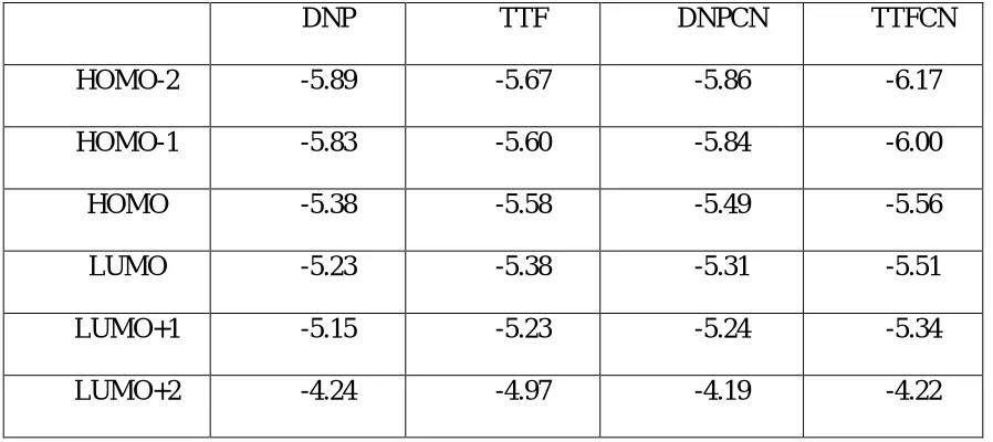
Table S1. The calculated orbital energies (eV) of rotaxane components.
DNP TTF DNPCN TTFCN
HOMO-2 -5.89 -5.67 -5.86 -6.17
HOMO-1 -5.83 -5.60 -5.84 -6.00
HOMO -5.38 -5.58 -5.49 -5.56
LUMO -5.23 -5.38 -5.31 -5.51
LUMO+1 -5.15 -5.23 -5.24 -5.34
LUMO+2 -4.24 -4.97 -4.19 -4.22
Table S1 lists the frontier MOs of DNP, TTF, DNPCN and TTF(CN) components. The characteristics of these MOs are shown in Figure S4, S5, S6 and S7 respectively. The characteristics of those MOs explain the mechanism of the different conductivities, for each switchable state of the rotaxanes.
Figure S4, S5, S6, and S7 show the frontier MOs of R-DNP, R-TTF, R-DNPCN, and R-TTF(CN) respectively.
The HOMO, LUMO and LUMO+1 of R-DNP are all delocalized orbitals. The HOMO, LUMO, LUMO+1 of R-TTF are localized molecular orbitals.
transmission, as shown in Figure S9. LUMO and LUMO+1 are localized MOs. HOMO and HOMO-1 are localized at Au electrodes.
Figure S8 shows the I-V curves as discussed in the Text. The left I-V curve for DNP-CN shows two flat regions from contributions from two frontier MOs. The right I-V curve shows below 0.1 V DNP has a large slope comparing with the curve after 0.1 V, indicating that two different MOs contribute to this curve. Thus the modification by CN changes the ON/OFF ratio, even though the electronic conductivity does not change significantly. This means that the mechanism of the switch in conductivity is dominated by the shape of the MO instead of its MO energy level.
Figure S9 shows the transmission function of DNP, TTF, DNPCN and R-TTF(CN) respectively. Each MO contributes a different transmission probability.
For R-DNP, the HOMO, LUMO and LUMO+1 are delocalized MOs and thus have 10-2 to 10-4 transmission probability.
However, the HOMO-2, LUMO and LUMO+1 of R-TTF only have ~10-5 transmission. The characteristic of the MOs in Figure S6 and Figure S7 clearly show the difference in localization of the MOs. The HOMO and HOMO-1 of R-TTF have small transmission probability because they are both localized Au orbitals. Similarly, the HOMO-1 of R-DNP leads to low transmission probability. The frontier orbitals of the CN modified rotaxane molecules are shown in Figure S3. We see that the LUMO+1 in R-DNP has become the LUMO in R-R-DNPCN leading to increased delocalization. This leads to improved conductivity.
R-25
from 0.06 to 0.20 nA/V. In contrast, the conductivities of R-DNP and R-DNPCN range from 1.00 to 9.0 nA/V. The peaks at around 0.2 V of R-DNP are dominated by the HOMO of R-DNP. The peaks at 0.0V and 0.40 V of R-DNPCN conductivities are contributed from LUMO and HOMO of R-DNPCN.
ON
HOMO HOMO-1
R-DNP
ON
R-DNP
27
OFF
HOMO HOMO-1
R-TTF HOMO-2
OFF
R-TTF
[image:32.612.133.489.67.689.2]LUMO LUMO+1
ON
HOMO HOMO-1
R-DNPCN
ON
R-DNPCN
29
OFF
HOMO HOMO-1
R-TTFCN
OFF
R-TTFCN
LUMO LUMO+1
-2.0 -1.5 -1.0 -0.5 0.0 0.5 1.0 1.5 2.0
-1.0 -0.5 0.0 0.5 1.0
applied bias (V)
Curren t (nA) R-DNP R-TTF R-DNPCN R-TTFCN (a) R-DNP R-DNPCN R-TTF, R-TTFCN -1.0 -0.8 -0.6 -0.4 -0.2 0.0 0.2 0.4 0.6 0.8 1.0
-0.2 -0.1 0.0 0.1 0.2
applied bias (V)
Current (nA) R-DNP R-TTF R-DNPCN R-TTFCN (b) R-DNP R-DNPCN R-TTF, R-TTFCN 20 30 40 50 60
-0.5 0.0 0.5
Applied bias (V)
On/Off Ratio (c) R-DNP/ R-TTF R-DNPCN/ R-TTFCN
31 1.E-07 1.E-06 1.E-05 1.E-04 1.E-03 1.E-02
-5.80 -5.60 -5.40 -5.20 -5.00
energy (eV)
Tran
sm
ission Function T(E)
R-DNP R-TTF HOMO: -5.38eV LUMO -5.22eV 10-2 10-3 10-4 10-5 10-6 10-7 LUMO+1: -5.15eV LUMO: -5.38eV LUMO+1: -5.23eV HOMO-2 -5.67eV 1.E-07 1.E-06 1.E-05 1.E-04 1.E-03 1.E-02
-5.80 -5.60 -5.40 -5.20 -5.00
energy (eV)
Tran
sm
ission Function T(E)
R-DNPCN R-TTFCN 10-2 10-3 10-4 10-5 10-6 10-7 HOMO -5.49eV LUMO -5.31eV LUMO+1 -5.24eV LUMO: -5.51eV LUMO+1 -5.34eV
0.00 1.00 2.00 3.00 4.00 5.00 6.00 7.00 8.00 9.00 10.00
-0.50 -0.30 -0.10 0.10 0.30 0.50
applied bias (V)
Condu
ctivity
(n
A/V)
0.00 0.02 0.04 0.06 0.08 0.10 0.12 0.14 0.16 0.18 0.20
-0.50 -0.30 -0.10 0.10 0.30 0.50
applied bias (V)
Condu
ctivity
(n
A/V)
R-33 0
40 80 120
-6.00 -5.80 -5.60 -5.40 -5.20 -5.00
energy (eV)
Den
s
it
y of States
R-DNP
R-TTF
HOMO-2
LUMO LUMO+1
HOMO
LUMO+1
LUMO
0 40 80 120
-6.00 -5.80 -5.60 -5.40 -5.20 -5.00
energy (eV)
Den
s
it
y of States
R-DNPCN
R-TTFCN
LUMO LUMO+1
HOMO
LUMO+1
LUMO
C h a p t e r I I I
ULTRAFAST PROTON-HOPPING MOLECULAR SWITCH †
Abstract
We propose the proton-hopping concept for ultrafast switching devices and test the design using a combination of computational approaches. As a specific implementation of a proton-hopping molecular switch, we consider a benzenamine component with two OH groups. Using transition state theory with quantum mechanical energy surfaces we predict that this design will lead to an Off to On switching speed of 3.65 picosecond and an On to Off switching speed of 8.6 picosecond. We find that an electric field of 1V/Å is sufficient to switch Off to On. Using Green’s function theory we find an On/Off ratio of ~ 5 in the conductivities.
Figure for Table of Contents (ultrafast proton-hopping molecular switch).
N
N
O H O
H
N
N
O H O
H
N
N
O H O
H
N
N
O H O
H S
S
S
S
S
S
S
S
Contact
Off On
z axis
Contact Contact
Contact
Contact Contact
35
The use of molecules as the active components of electronic devices was proposed in 1974 [1]. However, it is only until recently that the manufacture of single molecule devices becomes possible with the advances in nanotechnology. Several functionalities and phenomena useful for electronic applications have been demonstrated. These include resonant tunneling, Coulomb blockade and Kondo effect, etc.[2] A molecular switch based on a bistable rotaxane consisting of a ring and a backbone component was proposed and demonstrated,[3-5] where the writing voltage triggered the ring movement along the backbone between two stable states, leading to a dramatic change in the conductivity of the system that can be ascertained under a much smaller reading voltage. Although appealing as a memory device, the response time scale of this switch is too slow, ~ microseconds, limiting its application for ultra-fast process required by information technology for its next generation electronic devices. In this chapter, we discuss a new concept for an ultra-fast molecular switch triggered by proton migration. We designed a model system based this concept and validated it by using first principles calculations.
For a rational design of a molecular switch, two issues have to be considered: an ultra-fast response time scale and a switchable conductivity with changes of voltages. It is well known that proton hopping in aqueous solutions can occur at subpicoseconds or faster;[6-7] and that the conductivity of conducting polymers can change dramatically as a function of pH (On/Off ratio can be up to 1011), implying that proton motion may play an important role in changing electronic conductivity.[8] Therefore, it is possible to design an ultra-fast molecular switch triggered by proton migration.
Scheme 1 shows an example that may satisfy these two criteria. Under an applied field the proton can shift between oxygen and nitrogen atoms. When the proton is on nitrogen atom, the resonant structures allow delocalization of the electrons, leading to a higher conductivity. The proton migration potential is changed by the external electric field along the z axis of the molecule, allowing this voltage to control the On/Off of this switch.
point calculations are performed on the respective structures with the external electric field being turned on. The proton hopping rate was calculated using transition state theory (TST) based on the quantum mechanic results to estimate the vibrational frequencies and tunneling factors.[10] The electric conductivity was calculated directly from electronic wave functions using a full quantum-mechanical treatment combined with green function theory, as demonstrated by Ratner and Datta et. al.[12-15]
Figure 1 shows the potential energy surface for proton migration between the bistable sites. The Off state has two protons connecting to the oxygen atoms while the On state has both protons connecting to the nitrogen atoms. The Middle state has one proton connecting with the oxygen atom and the other connecting with the nitrogen atom. The blue curve is for zero voltage and the pink curve is the potential energy surface under an applied electric field (1V/Å). We find that this modest voltage is sufficient to change the relative stability of these three locally stable states.
Without an external field, the Off site is 12.01 kcal/mol more stable than the On site. The proton hopping barriers on the pathway are 9.33 kcal/mol from Off to Middle and 6.44 kcal/mol from Middle to On. The corresponding reverse hopping barriers are only 1.72 and 2.04 kcal/mol. After applying an electric field along the molecule axis, the potential energy surface changes. The On site is now 19.21 kcal/mol more stable than the Off state. TS1 presents no barrier from Off to Middle; while the hopping barrier for the second proton from Middle to On is only 1.67 kcal/mol.
The response time is a most important parameter for fast switching applications. The hopping rate can be estimated by using Transition State Theory with tunneling corrections. [10]
) exp(
) (
RT G h
T k T
k B
≠ ∆ − =κ
37 2
) ( 24
1 1 ) (
T k h T
B
≠ +
= ν
κ
With the voltage (1V/Å) applied to the molecule, the protons hop from Off to the On state, following the pink curve in Figure 1. The calculated hopping rate is 2.74×10¹¹
s-1, corresponding to a 3.65 ps switching speed. This is 106 faster than the rotaxane molecular switch. When the voltage is turned off, the switch goes from On to the Off state, as indicated in the blue curve of Figure 1. The calculated switching speed is ~ 8.60 ps. Therefore; this molecular switch exhibits an ultrafast switching speed needed in many application areas.
Figure 2A shows a prototype for a proton-hopping switch. The self-assembly monolayer forms between two Au thin films. The writing voltage controls proton migration while the reading voltage is used to detect the status of the switch. Our simulations used a simplified device with a dithiolate-benzenamine molecule with additional OH groups placed between the gold electrodes. The electrodes were modeled using clusters with three gold atoms. B3LYP/LACVP**[9] was used to calculate the Fock matrix and overlap matrix. Then Green’s function theory was used to calculate the transmission function and current. The current/voltage diagrams for the On and Off states were shown in Figure 2B, from which we see that under 0.5 V bias, the On/Off ratio can reach 5.
conjugated structures. We could use the present methodology to screen the choices for these to improve the performance.
Summary, we present a rational design strategy for ultra-fast molecular switches modulated by proton migration. This design was validated with first principles simulations, proving the good performances. Such switches should be useful for achieving the high switching speeds required by information technology for its next generation electronics.
ACKNOWLEDGMENT We thank Fraser Stoddart at UCLA for helpful discussions. This research was supported by the MARCO project at UCLA.
Reference
1. Aviram, A.; Ratner, M. A. Chem. Phys. Lett. 1974, 29, 277.
2. Aviram A.; Ratner, M.A. and Mujica, V. Molecular Electronics II NY Academy of Sciences, New York, 2002.
3. Collier C.P.; Wong E.W.; Belohradsky M.; Raymo F.M.; Stoddart J.F.; Kuekes P.J.; Williams R.S.; Heath J.R., Science 1999, 285, 391.
4. Collier C.P.; Jeppesen J.O.; Luo Y.; Perkins J.; Wong E.W.; Heath J.R.; Stoddart J.F.; J. Am. Chem. Soc. 2001, 123, 12632.
5. Luo Y., Collier C. P., Jeppesen, J. O., Nielsen K. A., Delonno, E. and et. al Chemphyschem 2002, 3, 519
6. Mauerhofer, E. and Ro¨sch, F. Phys. Chem. Chem. Phys., 2003, 5, 117–126. 0.69ps reported.
7. Horsewill, J.; Jones, N. H. and Caciuffo, R. Science 2000, 291, 100
39
9. The quantum calculations are performed by using Jaguar 5.0, from Schodinger Inc., Portland, Oregon.
10. Gonzalez, C. A.; Allison, T. C. and Louis, F.; J. Phys. Chem. A 2001, 105, 11034-11040.
11. Damle, P.; Ghosh, A.W. and Datta, S. Chem. Phys. 2002,281, 171–187
12. Datta, S. Electronic Transport in Mesoscopic Physics; Oxford University Press: Oxford, 1997.
13. Mujica, V.; Kemp, M.; Ratner, M.A. J. Chem. Phys. 1994, 101, 6849 14. Xue, Y.Q.; Datta S.; Ratner, M.A. J. Chem. Phys. 2001, 115, 4292
Scheme 1. Design strategy for proton-induced molecular switch. Proton hopping from Oxygen to Nitrogen under electric field leads to the change of conductivity. The product structure involves resonance among three valence structures.
N
N
O H O
H
N
N
O H O
H
N
N
O H O
H
N
N
O H O
H S
S
S
S
S
S
S
S
Contact
Off
On
z axis
Contact Contact
Contact
Contact Contact
41
-20
-15
-10
-5
0
5
10
15
20
Reaction Coordinate
Relative energy (
Kcal/mole)
TS
1(9.33)
TS
2(13.73)
Off
(0.0)
On
(12.01)
M iddle
(7.29)
Off
←
On 8.60 ps
TS
1(-4.72)
M iddle(-13.07)
TS
2(-11.40)
On
(-19.21)
Off
→
On 3.65 ps
-8 -4 0 4 8
-0.5 -0.3 -0.1 0.1 0.3 0.5
Voltage (V)
curren
t (µ
A) ON
OFF
0 2 4 6
0.0 Voltage(V)0.5
ON/OFF ratio
[image:47.612.110.501.66.551.2]43
Support information:
Ultrafast proton-hopping molecular switch Abstract
Section 1. Optimized structural information and energetics of proposed structures. 1.927 0.985 1.994 0.981 1.348 1.385 1.313 1.301 1.399 1.455 1.353 1.465 1.446 1.360 1.428 1.412 1.390 1.396 1.393 1.402 1.927 0.985 1.994 0.981 1.348 1.385 1.313 1.301 1.399 1.455 1.353 1.465 1.446 1.360 1.428 1.412 1.390 1.396 1.393 1.402 1.908 1.874 1.254 1.365 1.349 1.311 1.445 1.363 1.441 1.423 1.369 1.488 1.413 1.378 1.443 1.473 1.336 1.427 1.370 1.393 0.985 1.908 1.874 1.254 1.365 1.349 1.311 1.445 1.363 1.441 1.423 1.369 1.488 1.413 1.378 1.443 1.473 1.336 1.427 1.370 1.393 0.985 1.037 1.878 1.936 1.251 1.356 1.370 1.339 1.415 1.374 1.440 1.397 1.413
1.4881.414 1.377
1.445 1.504 1.256 1.429 1.369 1.403 1.037 1.878 1.936 1.251 1.356 1.370 1.339 1.415 1.374 1.440 1.397 1.413
1.4881.414 1.377
1.445 1.504 1.256 1.429 1.369 1.403
Off Middle On
1.262 1.925 1.252 1.359 1.357 1.321 1.424 1.369 1.441 1.413 1.384 1.484 1.414 1.376 1.445 1.493 1.290 1.429 1.369 1.397 1.295 1.262 1.925 1.252 1.359 1.357 1.321 1.424 1.369 1.441 1.413 1.384 1.484 1.414 1.376 1.445 1.493 1.290 1.429 1.369 1.397 1.295 1.909 1.316 1.290 1.368 1.329 1.306 1.451 1.360 1.452 1.433 1.364 1.462 1.409 1.384 1.416 1.478 1.336 1.417 1.383 1.394 0.985 1.247 1.909 1.316 1.290 1.368 1.329 1.306 1.451 1.360 1.452 1.433 1.364 1.462 1.409 1.384 1.416 1.478 1.336 1.417 1.383 1.394 0.985 1.247
45
Off state On state
[image:50.612.164.451.101.414.2]
Table 1. The energetic of quantum mechanics results.
Off(H-O) TS1 Middle TS2 On(H-N)
Energy E0 (under zero field) (Hartree)
-954.2940 -954.2748 -954.2833 -954.2691 -954.2787
ZPE (kcal/mole) 184.894 182.146 185.449 182.965 187.321 Relative energy ∆E0
without field (kcal/mole)
0 9.330 7.287 13.730 12.009
Gibbs Free Energy G (kcal/mole)
-28.360 -28.262 -28.513 -28.219 -28.252
Imaginary Frequency of TS (cm-1)
-2105.36 -1836.69
Energy Ef (under 1V/Å field) (Hartree)
-954.4452 -954.4483 -954.4669 -954.4603 -954.4797
Relative energy ∆Ef
under field (kcal/mole)
0 -4.717 -13.073 -11.402 -19.214
47
Section 2. The estimation of Proton hopping rate constant
The proton hopping rate constant is calculated by ( ) exp( ) RT
G h
T k T
k B
≠
∆ − =κ
Where κ(T) is the tunneling effect determined by ( )2
24 1 1 ) (
T k h T
B
≠
+
= ν
κ kB is Boltzmann
constant, h is plank constant and ν≠ is imaginary frequency of TS.
The ∆G? without field is calculated by ∆G≠ij =Ei0 +Gi +ZPEi −Ej0−Gj −ZPEjwhere
E0 is the energy without field, G is the Gibbs free energy and ZPE is zero point energy. Those parameters are listed in Table 1.
The ∆G?
under field is calculated by f j j
j i i
f i
ij E G ZPE E G ZPE
G = + + − − −
∆ ≠ where Ef
Table 2. The parameters for calculate rate constant of each step
TS ∆G?
(kcal/mole)
Freq (cm-1)
Tunneling effect
Rate constant
(s-1)
Hopping speed
(ps) Under 1V/Å field
Off → Middle TS1* -4.620 -2105.36
Middle → On TS2 1.965 -1836.69 1.184 2.74 × 10¹¹ 3.65
Without field
On → Middle TS2 1.753 -1836.69 1.184 3.91 × 10¹¹ 2.56
Middle → Off TS1 2.294 -2105.36 1.242 1.65 × 10¹¹ 6.04
* The TS1 under electric field is not a real Transition State anymore. Thus we did not
49
Section 3. IV characteristic calculated by Green Function theory
Generally the current through molecules at is expressed as;[11-14]
∫
−∞∞ −= T E V f EV f EV dE
h e V
I( ) 2 ( , )[ 1( , 1) 2( , 2)] (1)
where fi is the Fermi-Dirac function for a voltage Vi at electrode i(1 or 2). The transmission function, T(E,V), is the sum of transmission probabilities of all channels available at energy E and is obtained through the Green function of molecule, GM, affected by electrode
contacts. )] , ( ) ( ) , ( ) ( [ ) ,
(E V Trace 1 V G E V 2 V G EV
T = Γ M Γ M+ (2)
Γi describes the coupling at electrode i.
The Green function of molecule in equation (2), GM, will be calculated from the molecular
Hamiltonian, HMM(V), i.e.,
= − − − − − = − + + − 2 2 21 2 1 12 1 1 1 2 2 2 1 1 1 1 0 0 ) ( G G G G G G G G G g H ES g E G M M MM M M MM MM τ τ τ τ (3)
The submatrixes G and g represent Green functions when interactions among subsystems are included or excluded, respectively. gi represents the electrodes and τi describe the metal-molecule coupling. HMM and SMM are the Fock and overlap matrices of the isolated
molecule, respectively and E is the electron energy. Therefore, solving eq 3 for GM, we
obtain
1 2
1 ]
[ − −Σ −Σ −
= MM MM
M ES H
G (4)
1 1 1 1
τ
g
τ
+
=
Σ
andΣ
2=
τ
2+g
2τ
2 (5)where Σi are the self-energy terms coupling between the molecule and the electrodes.
All the needed parameters can be obtained from the Fock and Overlap matrices based on DFT calculations. = 22 2 21 2 1 12 1 11 H H H H H H H H H F M M MM M M and
=
22 2 21 2 1 12 1 11S
S
S
S
S
S
S
S
S
S
M M MM M M (6)The metal-molecule coupling term τi can be determined by
1 1
1
=
ES
M−
H
Mτ
andτ
2=
ES
M2−
H
M2 (7)HMi are the coupling matrix element between electrode and molecules.
The coupling Γi appeared eq. 2 is given by
]
[ 1 1
1 + Σ − Σ =
Γ i and Γ2 =i[Σ2 −Σ2+] (8)
gi are surface green function of electrode. For Au it can be approximated as a diagonal
matrix with each element proportional to their local density of states.
= ... ... ... ... ... 0 0 .. 0 0 ... 0 0 d p S i g g g g (9)
51 i
gp =−0.0426π
i gd =−0.1778π
The program referred Huckel-IV2.0 code provided by Supriyo Datta’s group.
Conductivity G is define by:
G
=
dI
/
dV
Figure 3 shows the calculated conductivity. For On state, the peak at 0.3 V responds to the contribution of HOMO of the molecules.
0 5 10 15 20
-0.5 -0.3 -0.1 0.1 0.3 0.5
Voltage (V)
Conduc
tivity dI/dV (
µ
A/V)
. ON
[image:56.612.197.419.281.492.2]OFF
C h a p t e r I V
PREDICTIONS OF HOLE MOBILITIES IN OLIGOACENE ORGANIC SEMICONDUCTORS FROM QUANTUM MECHANICAL CALCULATIONS
Abstract
We estimate the hole mobility for oligoacene crystals using quantum mechanics (QM) to calculate the reorganization energy and electron transfer coupling matrix elements and molecular dynamics (MD) to do the thermal averaging. Using an incoherent transport model we calculate a hole mobility of 6.5 cm2/Vs for pentacene crystals at 300K. This can be compared to recent experimental results of 5 cm2/Vs. However we find that an alternative packing into the crystal could lead to a hole mobility of 15.2 cm2/Vs. This suggests that current materials might still be improved by a factor of ~3. Such calculations might be useful for finding solid state structures that would increase the hole mobility for use in high performance molecular devices.
53
IV-1. Introduction
There is a great deal of interest in developing materials suitable for cheap, flexible electronic devices (e.g., Smart Card, flexible displays). A critical problem here is achieving the ~ 10 cm2/Vs hole mobility required for integrated circuits based on organics. [4] Amorphous Si is sufficient but too expensive. Organic semiconductors could ultimately be cheap enough, but the mobilities are low (10-2 cm2/Vs for amorphous pentacene and up to 5 cm2/Vs in thin films) [1,-3]. Moreover, many display and memory applications require much faster devices and hence higher mobilities. This raises the question of whether additional modifications in the engineering design of organic semiconductors could improve performance by the factors required [3].
In order to investigate this issue we developed a quantum mechanical (QM) protocol to estimate the mobilities for organic crystals as a function of temperature and pressure and applied it to four oligoacenes (pentacene, tetracene, anthracene, and naphthalene) with structures shown in Figure 1. Our estimates suggest that for the bulk crystal the limiting mobility at 300K is ~ 6.5 cm2/Vs for atmospheric pressure, indicating that the current materials are close to the optimum. We suggest that these approaches to computational estimates may be useful for virtual screening to find new lead materials likely to provide the improved properties required for increased transport efficiency (for increased device speed), reduced power and avoidance of excessive heating in the promising new applications.
Section IV-2 describes the theoretical methodology, including calculations of reorganization energy, coupling matrix elements, and the incoherent transport model. Section IV-3 discusses the results calculated for the four oligoacenes. The conclusions are presented in Sec. IV-4.
IV-2. Theoretical Methodology
The charge carrier mobility provides the figure of merit for applications of organics in electronic devices. For p-type oligoacene derivatives the conductivity is dominated by transport of positive charges (holes) with mobilities (µ) in the range 10-2
reported for the thin film and crystalline phases of pentacene.[1-4] Unfortunately there remain conflicts between experimental measurements [6,7], making it essential to develop a solid theoretical basis for understanding the mechanisms dominating hole mobility.
Electronic band structure calculations have previously been used to predict charge transport in perfect crystals of pentacene. Cheng et al carried out band calculations for oligoacenes, which assuming a coherent model they used to predict thermal-averaged velocity–velocity tensors. Comparing these tensors to recent experimental data they concluded that the simple band model is unable to explain the temperature dependence of the charge carrier mobility in oligoacene crystal systems for temperatures higher than 150 K. [5] This suggests that dynamic structure disorder may invalidate the band transport model for temperature above 150K suggesting that hopping may be the dominant mechanism at room temperature.
Structural disorder decreases the charge carrier mobility, giving rise to photocurrent transients and frequency dependence in the charge carrier mobility. The disorder leads to a non-periodic structure that may cause the transport mechanism to switch from band-like transport at low temperature (little disorder) to a hopping mechanism at higher temperature. Here structural fluctuations resulting from twisting and sliding of the molecules could play a prominent role.
In order to obtain quantitative insight into the role of structural disorder on the mobility of charge carriers in pentacene, we use an incoherent hopping model to describe the hole mobilities of oligoacenes at room or higher temperatures. Our aims are
• to provide a simple way to predict accurate values of the coupling matrix elements and reorganization energies involved in hole transport and