University of Twente
MESA+ Institute for Nanotechnology
Faculty of Electrical Engineering, Mathematics and Computer Science
Department of Electrical Engineering
Transducer Science and Technology Research Group
The Documentation
of
A Large Range Multi-Axis Capacitive Force/Torque Sensor Using a
Single SOI Wafer by Alveringh et al.
Author
Dennis Alveringh
Abstract
A miniature silicon capacitive force/torque sensor is designed and realized to be used for biomechanical applications and robotics. The sensor is able to measure the forces in three directions and two torques
using four parallel capacitor plates and four comb-structures. Novel spring and lever structures are designed to separate the different force components and minimize crosstalk. The highly reproducible
fabrication process is based on deep reactive ion etching of the two outer layers of a single silicon-on-insulator wafer and uses only two masks. The sensor has a force range of 2 N in shear and normal direction and a torque range of more than 6 N mm. It has a high sensitivity of 38 fF N−1 and 450 fF N−1in shear and normal direction respectively. A calibration matrix is derived from the sensor’s
Contents
Introduction 1
1 Literature study 3
1.1 Introduction . . . 4
1.2 Capacitive force sensors with silicon springs . . . 6
1.3 Capacitive force sensors with polymer springs . . . 12
1.4 Piezoresistive force sensors with silicon springs . . . 18
1.5 Piezoresistive force sensors with polymer springs . . . 22
1.6 Conclusion . . . 24
2 Theory 25 2.1 Introduction . . . 26
2.2 Concepts for a six degrees of freedom stage . . . 27
2.3 Concepts for sensing structures . . . 31
2.4 Mathematical model . . . 32
2.5 Design of the suspended core . . . 38
2.6 Design of the sensing structures . . . 41
2.7 Conclusion . . . 45
3 Fabrication 47 3.1 Introduction . . . 48
3.2 Design of the fabrication process . . . 49
3.3 Fabrication report . . . 55
3.4 Discussion and conclusion . . . 59
4 Characterization 61 4.1 Introduction . . . 62
4.2 Characterization of the suspended core . . . 63
4.3 Characterization of the sensor . . . 65
4.4 Discussion and conclusion . . . 68
Conclusion 70
References 71
List of figures 74
A Symbols, quantaties and constants 77
B Paper for publication 80
C Conference abstract 91
Introduction
This documentation consists of four parts and several appendices that contain the details of the sensor proposed in the paper by Alveringh et al. [1]: A Large Range Multi-Axis Capacitive Force/Torque Sensor Realized in a Single SOI Wafer. It can be seen as an extension of the paper to provide details about the design, explain design choices and help reproducing the sensor.
This documentation is divided in four parts: theory, fabrication, characterization and literature study. Each part is a stand-alone report including an introduction and conclusion. The part ‘theory’ describes different concepts, a derivation of the mathematical model of the chosen concept and the details of all the design steps of the sensor. The part ‘fabrication’ describes the theory and the design of the fabrication steps and provides a report of the actual process. The part ‘characterization’ describes the measurement setup and results that characterizes the sensor. The part ‘literature study’ describes several other force/-torque sensors using different technologies.
Introduction to the subject
Miniaturized multi-axis force/torque sensors are widely used in medical applications, tactile sensing and robotics. Many prostheses, for example, require safe and comfortable interaction with people who underwent amputation of a part of a limb. Bad fitting between the socket of the prosthesis and the residual limb may cause pain and even damage to the underlying blood vessels [28, 25]. Measuring the shear forces and normal forces between the socket and the residual limb is possible with multiple small force sensors. The socket of the prosthesis can use this information to adjust the shape of the socket, making the load distribution as comfortable and healthy as possible.
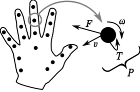
Other applications are in the field of characterization of the human body. For example, power measure-ments of the human hand are important for rehabilitation purposes or the optimization of the endurance of athletes [39]. These power measurements can be done with force/torque sensors, accelerometers and gyroscopes at each joint integrated in a glove (figure 1).
F
v ω
T P
Figure 1: Power measurements of the human hand using force sensors, accelerometers and gyroscopes. The powerP in one element is equal toF~ ·~v+T~·~ω.
Force sensors are also very interesting for robotics. Humanoid robots [19] or robotic hands [8] have to interact with the environment. Force sensors on top of the fingers and toes help the robot to measure load distributions on the hands and feet. Even the difference between rough and flat surfaces may be sensed by the robot.
For the three mentioned applications, a few specific requirements are applicable:
• the sensor should measure multiple (preferably six) degrees of freedom;
• the sensor is small, preferably less than 1 cm2with a thickness of less than 1 mm;
• the sensor should be able to handle human forces, i.e. at least a few newtons.
Commercially available non-MEMS load cells support high force ranges, but are often too large to integrate in the applications mentioned above. There are MEMS-based force and torque sensors available in literature, but many lack the support for measuring torques [13, 21] or forces [2]. Besides, many sensors only support forces in the milli newton or micro newton range [10, 29, 24]. The fabrication process of most MEMS-based sensors is still in an experimental stage [13, 21, 24, 36, 6], they use non-trivial polymer technologies or crucial wafer bonding steps in the process. The latter property makes the existing force sensors even less attractive, since above specified applications need tens of these expensive sensors per device.
1
Literature study
F
U
Author
Dennis Alveringh
PART 1. LITERATURE STUDY
1.1
Introduction
This literature study is orginally done as a preliminary exploration for the design and fabrication of a microelectromechanical system (MEMS) based force/torque sensor. The purpose of this part at the end of this documentation is to give a context for the realized sensor.
This literature study describes state-of-art MEMS force sensors with their performance, range, con-struction and fabrication. A selection is made based on the following two conditions:
• it uses fabrication technology existing in the MESA+ nanolab of the University of Twente, e.g. bulk
micromachining in silicon, wafer bonding and polymer deposition;
• the sensor should have at least one characteristic, and therefore inspiring, property for tactile
sensing, i.e. there should be support for multiple degrees of freedom and/or a large range of force. This part starts with a section where four different categories of sensors will be outlined. This part continues with brief summaries of the papers ordened per category. Especially the performance of the sensors, the design and the fabrication will be summarized. The author chose for small summaries of many different papers instead of extensive analyses of just a few papers.
Types of force/torque sensors
All force sensors in this part use the operating principle described in figure 1.1. A force is applied on a spring system which causes a displacement in the sensor structure. The sensing structures produce an electric quantity at the output (e.g. voltage, capacitance or resistance) directly dependend of the displacement.
Bell et al. of reference [3] published in 2005 an overview of the characteristics of actuators, force sensors and displacement sensors that were published last years. Since force sensors are most interesting for this study, only the results for the sensors will be shown here. Bell et al. divided the sensors in different working principles (capacitive and piezoresistive for example) and plotted the resolution and frequency in diagrams dependent of the force.
It seems that using capacitance as readout method is not common for forces above 1 mN, most designers chose for piezoelectric or piezoresistive materials in this range. But in fact, there are papers ([6] and [13] for example) published after this paper of Bell et al. with a capacitive readout and support for forces above 1 mN.
Although Bell et al. described more categories, this part has only four categories of MEMS sensors that can be made with the existing technology in the MESA+ nanolab. Table 1.1 shows the four categegories and their corresponding section in the part.
Table 1.1: Four types of force/torque sensors
1.1. INTRODUCTION
force
springs
sensing structures displacement
electric quantity
readout electronics
value
capacitive
piezoresistive
C
R
silicon
polymer
sensor
Figure 1.1: Common operating principle of MEMS force sensors.
(a) Resolution versus maximum force of sensors.
(b) Frequency versus force of sensors.
Source: Bell et al. [3]
PART 1. LITERATURE STUDY
1.2
Capacitive force sensors with silicon springs
Capacitive force sensors are using a change in capacitance as measurement for force, caused by a clos-ing/opening gap between or change in overlapping area of electrodes. Silicon is used for the springs of all sensors in this section. It has a high Young’s modulus and yield strength compared to polymers and many metals. Silicon is able to survive high stresses and is therefore a suitable material for large range force sensors. This section describes several sensors using a silicon spring system and capacitive readout.
Wiegerink et al. presented a silicon based capacitive load cell [42] in 2000 that was able to measure loads up to 10 kN. The sensor consists of a top and bottom electrode seperated by a spring. A normal force results in a reducing change in gap and increasing capacitance between the two electrodes. The spring consists of several silicon pillars that can be compressed. The electrodes are located between the pillars. The structures were made in two wafers which were bonded together.
Brookhuis et al. of the same research group developed a more advanced version of the sensor in 2012. The paper in reference [6] presents a force sensor that is capable of measuring normal force and torque around two axes. Even though the sensor has multiple degrees of freedom, it can handle large forces: 50 N of normal force and moments can be measured up to 25 N mm and is therefore proposed as a sensor for biomechanical applications. The sensor uses the same spring system as Wiegerink et al., but now the pillars can bend to make shear displacements possible. The bottom electrode consists of four quadrants to distinguish the different directions.
Fabrication is done using a highly doped silicon top wafer and a silicon on insulator (SOI) bottom wafer. Deep reactive ion etching (DRIE) is used to create the pillar spring elements. The bonding of the wafers is based on silicon fusion bonding.
1.2. CAPACITIVE FORCE SENSORS WITH SILICON SPRINGS
Source: Wiegerink et al. [42]
Figure 1.3: The quasi-monolithic silicon load cell for loads up to 1000 kg with insensitivity to non-homogeneous load distributions from Wiegerink et al.
Q1 Q3
q
Q1 Q2
Q3
Q4
2Lq θ
(a) Principle of operation with silicon pillars and electrodes in four quadrants.
f
(a)
(b)
(c)
(d)
(e)
(f)
(g)
(h)
(i)
(l) (m)
(j)
(k)
pillar cap. area
(b) Fabrication, the materials are color coded with legend in the figure.
(c) Photo of the device.
Source: Brookhuis et al. [6]
PART 1. LITERATURE STUDY
As Brookhuis et al. uses parallel plate capacitors and springs under the end-effector, Sun et al. proposes a completely different sensor in 2002. This sensor is two degrees of freedom and has edge-supported springs. It has comb-structures in two orientations to measure two shear forces. It is developed for purposes as biomaterial characterization and material science.
The same research group improved the design with Beyeler et al. in 2009 by making the sensor capable of measuring in six degrees of freedom up to 1000 µN for translations and 2.6 mN mm for rotations with micro-newton and nano-newtonmeter resolution respectively. This sensor consists of a movable body of silicon supported by four springs in the same horizontal plane. Multiple capacitors are used for readout and determine the direction of displacement of the movable body. Parallel plate capacitors parallel to the body and the bulk change in gap due to normal forces and torques and can be measured differentially. Finger shaped capacitors change in gap by in-plane movements and can be measured differentially.
1.2. CAPACITIVE FORCE SENSORS WITH SILICON SPRINGS
(a) Principle of operation, all degrees of freedom are shown with their increase or decrease in capacitance.
(b) Fabrication.
(c) Photo of the device.
Source: Beyeler et al. [5]
PART 1. LITERATURE STUDY
The earlier described sensors are six degrees of freedom sensors. Following sensors are only one degree of freedom sensor, but have other unique properties.
The sensor of Chu et al. published in 2007 [10] has an overall dimension of 3.6 mm by 1 mm by 10 µm and is designed for purposes as micro-assembly and living cell manipulations. This sensor measures force in one direction, but has thanks to a displacement reduction mechanism and finger-shaped capacitors a very high accuracy. The maximum force is 11 mN. The capacitance change with this force is about 175 fF to 200 fF. The sensor consists of a lever system that reduces the displacement due to the applied force and transforms it to a horizontal displacement moving two set of combs closer to the anchored combs. This increases the capacitance.
Fabrication is started by patterning and etching a glass wafer. Then, single crystal silicon is anodically bonded to the glass wafer. A metal layer is deposited for better electrical conductivity. The silicon with metal is etched to form the device.
Muhammad et al. made in 2011 a sensor with multiple elements of one degree of freedom and with support to forces up to 24 mN. It is developed for a biomimetic fingerpad. Typical of the sensor is the very cost-efficient fabrication. Each element consists of an edge supported stage. Bending of the stage causes a closing gap and increasing capacitance.
1.2. CAPACITIVE FORCE SENSORS WITH SILICON SPRINGS
(a) Overview and principle of operation. (b) Photo of the device.
Source: Chu et al. [10]
Figure 1.6: Design of a high sensitivity capacitive force sensor from Chu et al.
(a) Principle of operation.
(b) Fabrication.
Source: Muhammad et al. [29]
PART 1. LITERATURE STUDY
1.3
Capacitive force sensors with polymer springs
The paper in [27] by L¨otters et al. describes as one of the first papers (1999) the polymer polydimethyl-siloxaan (PDMS) as a mechanically interesting material for MEMS. It begins with mechanically interesting facts about PDMS: it’s unique flexibility between 100 kPa and 3 MPa for example. The experiments with the results that are proposed in this paper are mainly about the performance of PDMS when it comes to usage in microfabrication. PDMS was spun upon wafers with varying speeds between 1000 rpm and 5000 rpm with 20 s and 60 s spin time. The coating was exposed to UV light and was cross linked. The thickness dependent on the speed and time are plotted in figure 1.8a. The shear modulus dependent on the frequency (figure 1.8b) and temperature (figure 1.8c) are measured using two discs with PDMS between them. A torque is applied on one of the discs and the movement due to this torque is measured. It appears that the frequency has no effect on the shear modulus. The temperature has a linear positive effect on the shear modulus. The adhesion of PDMS on silicon oxide after using a primer (TMSM) is very good following to L¨otters et al. It was not possible to separate the PDMS from the silicon with manual peel tests. Adhesive strenghts up to 180 kPa with PDMS on a polished surface were measured.
1.3. CAPACITIVE FORCE SENSORS WITH POLYMER SPRINGS
(a) Characteristics of spinning PDMS. (b) Shear modulus dependent on the frequency
(c) Shear modulus dependent on the temperature.
Source: L¨otters et al. [27]
Figure 1.8: The mechanical properties of the rubber elastic polymer polydimethylsiloxane for sensor applications from L¨otters et al.
(a) Measurement setup.
0 1 105 2 105
3 105
0 0.04 0.08
y = 76979 + 2.6304e+06x R= 0.99995
S
tr
e
s
s
,
P
a
Strain
(b) Strain-strain relation of PDMS.
Source: Wang [41]
PART 1. LITERATURE STUDY
SU-8 is another polymer that may be used as spring material for force sensors. It’s Young’s modulus is much higher than the one of PDMS (more than 4·103times higher). However, SU-8 can be patterned with very high aspect ratios. There is a bonding step needed to mount the end-effector of the sensor to the SU-8 pattern. This crucial fabrication step is analyzed in literature.
Pan et al. [32] patterned several materials on two silicon wafers with photolithography in 2002. The two wafers were bonded using the commercial available EV501 bonder. There is no voltage applied to the wafers. The bonding temperature and the bonding force are varied and the effects of these parameters are shown in figure 1.10b and figure 1.10c respectively. It is concluded in the paper that SU-8 is a very good bonding material due to it’s epoxy feature. There is also concluded that a layer thickness of 100 µm is possible.
An example of an early force sensor using a flexible spring system can be found in reference [9], already in 1995. Chase and Luo proposed a relative simple sensor design using a flexible layer enclosed by two capacitor plates. The sensor is capable of measuring normal and shear force. The range of operation is unknown for the authors only provide the displacement information of their sensor. The sensor consists of four bottom capacitor plates and a floating top capacitor plate. The plates are made on polyimide (PI) layers. Unfortunately, it is not given what the real spring material is.
An example of the full design process of a sensor based on PDMS can be found in reference [24] of 2008. The sensor is made for robotics and prosthetics. Lee et al. explains the design, fabrication and measurements of a force sensor with PDMS as spring material. A four by four array of these sensors was used to determine the range of 10 mN with sensitivities of 2.5% mN−1, 3.0% mN−1, and 2.9% mN−1 for the x-, y-, and z-directions, respectively. The sensor’s principle of operation is based on four air gaps in a polymer (PDMS). The polymer is flexible making the air gaps able to be compressed. There are capacitor plates above and below each air gap. Differential change in capacitance can be used to measure shear forces and common change in capacitance can be used to measure the normal force.
1.3. CAPACITIVE FORCE SENSORS WITH POLYMER SPRINGS
(c)
heater
heater
vacuum environment
(d) (a)
si si microstructure bottom substrate up substrate
(b) bonding pad finished products (a) Fabrication 0 30 60 90 120 150 180 210 240
0 20 40 60 80 100 120 140 160
Temperature (oC )
Bonding strength (
kg/cm
2)
SU8 SP-341 AZ-4620 JSR
(b) Tensile strength of the bond versus the bonding temperature. 0 30 60 90 120 150 180 210 240
0 1 2 3 4 5 6 7 8 9 10 11 12
Bonding force (x10N)
Bonding strength
(kg/cm
2)
SU8 SP-341 AZ-4620 JSR
(c) Tensile strength of the bond versus the bonding force.
Source: Pan et al. [32]
Figure 1.10: A low-temperature wafer bonding technique using patternable materials from Pan et al.
(a) Principle of operation, the four air gaps can become smaller or larger due to normal force or shear force making the ca-pacitances change.
(b) Fabrication.
Source: Lee et al. [24]
PART 1. LITERATURE STUDY
The sensor of reference [13] by Dobrzynska and Gijs in 2010 uses PI as spring material and has the ability to measure in one degree of freedom (normal force). Because of the higher stiffness of PI compared to the more trivial PDMS as spring material, the sensor can handle much higher forces: Dobrzynska and Gijs measured until 3 kN with a sensitivity of approximately 1 fF N−1. The goal for this sensor is that it will become a part of a measurement system for feet. Two levels of finger-like conducting microstructures form four redundant capacitors. The whole sensor is embedded in PI. The two levels of microstructures come closer when a force is applied. The bond pads are on the lower level; the authors made a via from the higher to the lower level.
The fabrication starts with a sacrificial layer of aluminum. PI was spun on top of this layer. Then, the lower electrode was sputtered. The second layer of PI was spin coated and using a photoresist with a smooth slope, a slope was etched in the top layer of PI. The second electrode with via was sputtered after this. And finally, the last layer of PI was spun, openings for bond pads were etched and the sacrificial layer with wafer were removed.
Sensors with the measurement electronics on the same chip are not very common. Hence, one summary of such a sensor might be a good addition to this literature study. Liu et al. with the paper in reference [26] of 2011 describe the combined process of the fabrication of the micro mechanics in combination with CMOS1. The designers measured the sensors with different thicknesses of the flexible layer, the most robust sensor had a range of 2.4 mN and a sensitivity of 1.5 mV mN−1. The sensor works simply with multiple floating capacitor plates buried in PDMS arranged in a circular formation. Capacitor plates below the polymer are connected to the readout electronics made of CMOS.
The whole sensor is made using surface micromachining. The designers did not do the CMOS pro-cess themselves, this is done by an external company. Fabrication of the capacitor plates is done in the CMOS process. The holes are etched and the PDMS polymer is cast between the capacitor plates by the designers themselves.
1.3. CAPACITIVE FORCE SENSORS WITH POLYMER SPRINGS
(a) Schematic view of the top electrodes with via and bottom electrodes.
(b) Fabrication.
Source: Dobrzynska and Gijs [13]
Figure 1.12: Capacitive flexible force sensor from Dobrzynska and Gijs.
(a) Overview with the principle of operation. (b) Fabrication after the CMOS process.
Source: Liu et al. [26]
PART 1. LITERATURE STUDY
1.4
Piezoresistive force sensors with silicon springs
Another common way for readout of force sensors is using piezoresistive elements. These elements change in resistivity dependent of the applied stress. The design of these sensors are quite different than capac-itive sensors, for the elements itself must be deformed.
In 2005, Beccai et al. came with a three-axial force sensor made in silicon and uses piezoresistive elements for measurements. It was developed for biomechanical measurements for prosthetics. The sensing chip consists of a stylus mounted on a plus-shaped spring alowing the three translations. There is a carrier chip that is connected by flip-chip bonding on the sensing chip. This method allows a thin sensor which makes it suitable for flexible skin implementation in prosthetics. The mechanical structures in the sensing chip was made using Advanced Silicon Etching, a deep dry etching process, in a SOI wafer. The p-type piezoresistors were obtained by ion implantation of boron. The sensor can manage forces until 2 N in all directions with high linearity (better than 99 %).
1.4. PIEZORESISTIVE FORCE SENSORS WITH SILICON SPRINGS
Source: Beccai et al. [2]
Figure 1.14: Design and fabrication of a hybrid silicon three-axial force sensor for biomechanical appli-cations from Beccai et al.
(a) Overview. (b) Fabrication.
Source: Wisitsoraat et al. [43]
PART 1. LITERATURE STUDY
The sensor proposed in [38] by Tibrewala et al. in 2008 was made with bulk micromachining, like Beccai et al. did, but has a different and less complicated fabrication process. It also features experi-ments how the piezoresistors should be placed on the beams. It concludes that the T-form placement has the highest sensitivity in both directions. The sensor can handle a maximum force of 25 mN in all directions. Fabrication is done using an n-type wafer with a patterned layer of silicon dioxide. p-Diffusion is performed to form the strain gauges. KOH etching is used at the bottom of the wafer to form the plus-shaped spring.
The sensor in [40] by Wang et al. in 2009 is another plus-shaped sensor. Characteristic of the sensor is it’s application: it is designed for minimally invasive surgery. The sensor is tested until 1 mN and performed with a better resolution than 3 µN.
1.4. PIEZORESISTIVE FORCE SENSORS WITH SILICON SPRINGS
(a) Principle of operation. (b) Fabrication. (c) Piezoresistor placement: 1 is transversal, 2 is longitu-dinal, 3 is T-form and 4 is quadratic configuration.
Source: Tibrewala et al. [38]
Figure 1.16: Simulation, fabrication and characterization of a 3D piezoresistive force sensor from Tibre-wala et al.
(a) Overview with the pattern coded materials. (b) Fabrication. For details, see [40].
Source: Wang et al. [40]
PART 1. LITERATURE STUDY
1.5
Piezoresistive force sensors with polymer springs
One can use polymer springs for force sensors instead of silicon springs in combination with piezoresistive elements, just as described previously with capacitive readout. But, because piezoresistive elements are flexible too, the complete sensors can be made flexible. Hwang et al. proposes a sensor [21] in 2007 that is completely flexible and is applicable in robotics. The sensor can handle 4 N of normal and shear force. Quantitative sensitivity information is not mentioned in the paper, but it is said that it is relatively low and the sensor is therefore inaccurate for small loads. Sensing is done with four strain gauges between a top layer of PDMS and a bottom layer of PI. Electrical connections on the top layer are connected to the strain gauges using vias.
A layer of PI is spin coated on a silicon wafer with a small layer of silicon dioxide. After patterning the gauges and electrical interconnections, the PI layer is released from the silicon wafer by etching out the silicon dioxide layer. The PI layer with strain gauges is attached on a ductile PDMS substrate using adhesive Kapton film.
A completely different way of using piezoresistive elements in a flexible material is done by Takei et al. Takei et al. present a sensor [36] in 2012 based on a flexible polymer layer for lingual motion sensing. The paper describes measurement results of shear stresses and pressures that occur in the mouth by humans swallowing water. The sensor should withstand therefore a shear stress of 2 kPa and a pressure of 20 kPa. The principle of operation is based on three piezoresistive cantilevers oriented in three directions immersed in PDMS. Two cantilevers are folded in vertical direction to measure the shear forces. The third cantilever is similar to a bending bridge and measures the normal force.
1.5. PIEZORESISTIVE FORCE SENSORS WITH POLYMER SPRINGS
(a) Overview, with the sensing structure on top of the PI layer.
(b) Principle of operation. (c) Photo of the device with a grid of sensing devices.
Source: Hwang et al. [21]
Figure 1.18: A polymer-based flexible tactile sensor for both normal and shear load detections and its application for robotics from Hwang et al.
(a) Principle of operation with specification of the materials.
(b) Photo of the device.
Source: Takei et al. [36]
PART 1. LITERATURE STUDY
1.6
Conclusion
This part summarized the working principles, fabrication and performance of 15 sensors. All sensors are categorized in four categories: capacitive force sensors with silicon springs, capacitive force sensors with polymer springs, piezoresistive force sensors with silicon springs and piezoresistive force sensors with polymer springs.
All sensors met the requirements for this literature study: all sensors can be fabricated with the technology that exists in the MESA+ nanolab of the University of Twente and all sensors have at least one characteristic property for tactile sensing.
The sensors are summarized in table 1.2.
Table 1.2: Overview of the force sensors described in this part.
Author Year DOFa Spring material Outputb Rangec Performancecd Brookhuis et al. 2012 6 Silicon Capacitive 10 N 16 pF N−1
Beyeler et al. 2009 6 Silicon Capacitive 1 mN 1 µN
Muhammad et al. 2011 1 Silicon Capacitive 24 mN N/Ag
Chu et al. 2007 1 Silicon Capacitive 11 µN 18 fF mN−1
Lee et al. 2008 3 PDMS Capacitive 10 mN 2.5 % mN−1
Dobrzynska and Gijs 2010 1 PI Capacitive 3 kN 1 fF N−1
Liu et al. 2011 1 PDMS Capacitivee 2.4 mN 1.5 mV mN−1
Chase and Luo 1995 1 N/Ag Capacitive N/Ag N/Ag
Beccai et al. 2005 3 Silicon Piezoresistive 2 mN <1 % Tibrewala et al. 2008 3 Silicon Piezoresistive 25 mN N/Ag
Wang et al. 2009 3 Silicon Piezoresistive 1 mN 3 µN
Wisitsoraat et al. 2007 3 AlN Cr/Al Piezoresistive 1 µN 0.2 mV µN−1
Takei et al. 2012 3 PDMS Piezoresistive 2 kPa N/Ag
Hwang et al. 2007 3 PDMS Piezoresistive 4 N N/Ag
aDegrees of freedom.
bQuantity that is measured at the output of the sensor.
cFor 6DOF and 3DOF sensors in shear direction, for 1DOF sensors the supported direction. dCan be the sensitivity (in F N−1 for example), resolution (in N for example) or error (in % for
example).
eWith on-chip readout electronics.
f This is not a typographical error, the elastic material silicone is meant here. gNot available or not applicable.
Silicon based capacitive force sensors combine classical fabrication techniques with freedom in design. The sensing structures only need two capacitor plates which can be placed and oriented in several ways (e.g. parallel plates or combs). This literature study proves the very different possibilities for this category of sensors.
Capacitive sensors with polymer springs may allow even more freedom in design, since the capacitor plates are not forced to be supported by silicon structures but may be floating in a thick polymer layer. However, using polymers in sensors requires less trivial fabrication steps.
The freedom in design for piezoresistive silicon based force sensors is more limited. This literature study shows that most designers choose for a plus-shaped sensor with piezoresistive elements attached to the beams. The fabrication of piezoresistive force sensors is also not very diverse: the sensing structures are mostly made using surface micromachining (p-diffusion) and the mechanical structures is mostly made using a back etch in the wafer.
2
Theory
Author
Dennis Alveringh
PART 2. THEORY
2.1
Introduction
This part describes the full design flow for a capacitive force/torque sensor. Capacitive force/torque sensors use a spring mechanism to convert forces (or torques) in displacements. These displacements cause capacitor plates change in gap or change in overlapping area. The change in capacitance can be measured electrically.
Five requirements, which are derived from the requirements in the overall introduction, are taken as guideline through the design process:
• the sensor should be relatively trivial to fabricate using well-known technologies and the technology
should be highly reproducable, i.e. the fabrication should take less than two months;
• the sensor should support measurements in multiple degrees of freedom;
• the sensor should have a competing sensitivity, in comparison with with the sensors summarized in
the literature study;
• the sensor should be able to handle human forces, e.g. multiple newtons;
• the sensor should be small, preferable less than 1 cm2 with a thickness of less than 1 mm.
It is not possible to make above requirements more specific (e.g. give quantative values to the sensi-tivity or force range), since some requirements may interfere with other requirements.
2.2. CONCEPTS FOR A SIX DEGREES OF FREEDOM STAGE
2.2
Concepts for a six degrees of freedom stage
Most force sensors are based on measuring a displacement rather than the force directly. A system of springs convert the force to a displacement. This section describes multiple spring systems with their stiffness in shear and normal direction obtained by finite element method (FEM) simulations. Besides, the maximum stress of all concepts is determined. The concepts are briefly described; more detailed descriptions of the models and simulations are in section 2.5.
The simulations were done using COMSOL Multiphysics 4.3.0.151.
2.2.1
Bottom supported springs of SU-8
This concept is based on the negative photoresist SU-8 as spring material. Typical of SU-8 is that it can be patterned with very high aspect ratios. It’s Young’s modulus is 4.02 GPa and it’s maximum stress (after a hard bake) is 34 MPa [12]. The latter property must be interpreted as a guideline, as the material will fail with a different stress in different directions.
Stiffness
A model of a six degrees of freedom stage is made in COMSOL (figure 2.5). A cylinder of polysilicon with a diameter of 1 cm and thickness of 500 µm is used as stage. Several small pillars of SU-8 support the stage at the bottom. The number of pillars and the diameter of the pillars is swept and the stiffness and maximum stress is investigated. A diameter of 300 µm and a length of 300 µm for the pillars that are located in a grid with a distance of 1250 µm from each other turned out to have the optimal behavior. A stress of 12 MPa at maximum for 10 N of shear load with a stiffness of 12 N µm−1 is obtained. For a normal load of 10 N, a stress of 3.6 MPa at maximum with a stiffness of 50 N µm−1is obtained.
(a) Shear load of 10 N. (b) Normal load of 10 N.
Figure 2.1: FEM simulation of the bottom supported springs of SU-8 concept. The colors represent the von Mises stress in Pa.
Fabrication
Since SU-8 is a photoresist that can be patterned with very high aspect ratios, many mechanical structures are possible, e.g. mechanical application can be achieved like was done in reference [6]. However, a rigid stage is needed as end-effector of the sensor and must be bonded on top of the pillars. Two methods were reviewed for bonding a rigid stage to SU-8 pillars.
SU-8 bonding
SU-8 is an epoxy based material that may be bonded to another SU-8 layer under pressure and with the right temparature. Pan et al. did this for SU-8 layers of 100 µm [32]. A bonding strenght of 20.6 µm was measured in the publication. However, the bonding process with SU-8 is still not trivial microfabrication and may require many experiments before it can be used in the design of a force/torque sensor.
Through-hole mounting
PART 2. THEORY
will be filled with SU-8 and exposed through the holes of the top wafer. After development and rinsing, pillars of SU-8 are made between the two wafers.
It must be noticed that SU-8 has a high viscocity; it may be difficult to rinse away all the undeveloped SU-8.
(a)
(b)
(c)
(d)
(e)
(f)
(g)
silicon SU-8
exposed SU-8
(h)
Figure 2.2: SU-8 pillars in holes: (a) a silicon wafer, (b) etching holes in the wafer with small bumps at both sides of the chip, (c) bond the wafer on top of another silicon wafer, (d) fill the structure with SU-8, (e) expose SU-8 through the holes of the top wafer, (f) develop and rinse, (g) saw or etch the wafer in chips.
Capacitor integration
Capacitors may be made between the top and bottom layer. Patterning of SU-8 allows the capacitor structures be very close to eachother, which increases sensitivity.
2.2.2
Bottom supported springs of PDMS
Instead of SU-8 as spring material, another polymer can be used. Polydimethylsiloxane (PDMS) is a polymer with a very low Young’s modulus (750 kPa [27]) compared to other polymers. It’s stress/strain relation is linear until a stress of approximately 300 kPa [41].
Stiffness
In COMSOL, a stage of polysilicon with a diameter of 1.5 cm and thickness of 400 µm is modelled. A layer of PDMS acts as support and is directly mounted at the bottom of the stage. The PDMS layer has a thickness of 30 µm. The model turns out to have a stress of 238 kPa at maximum for 10 N of shear load with a stiffness of 1.5 N µm−1. For a normal load of 10 N, a stress of 58 kPa at maximum with a stiffness of 77 N µm−1 is obtained.
Fabrication
One solid layer of PDMS can be used as spring system, as is done in the simulation. But to achieve a sufficient capacitance over stiffness ratio, the layer of PDMS should be less stiff and the electrodes should be closer to eachother. Patterning PDMS can reduce the stiffness in all directions and allows close capacitor structures. For example, PDMS pillars can be made with capacitor electrodes between the pillars. Unfortunately, patterning PDMS is not as trivial as pattering a photoresist like SU-8.
Capacitor integration
2.2. CONCEPTS FOR A SIX DEGREES OF FREEDOM STAGE
(a) Shear load of 10 N. (b) Normal load of 10 N.
Figure 2.3: FEM simulation of the bottom supported springs of PDMS concept. The colors represent the von Mises stress in Pa.
(a)
(b)
(c)
silicon PDMS
(d)
Figure 2.4: PDMS sensor fabrication: (a) a silicon wafer (b) application of one solid layer of PDMS (c) bonding or growing another layer of silicon
2.2.3
Edge supported springs of silicon
Previous two concepts are bottom supported. A six degrees of freedom stage can be also supported at the edges. As silicon is the most trivial material for microfabrication, this material is taken as starting point. A circular six degrees of freedom stage needs a point symmetric system of springs which are compliant in two directions. The v-shaped spring is the simplest implementation that obeys above specifications.
Stiffness
A stage of polysilicon with a diameter of 2.5 mm and thickness of 380 µm is modelled as end-effector. The stage is supported by 15 v-shaped springs consisting of two right-angled flexures of 490 µm per flexure. A stress of 448 MPa at maximum with a stiffness of 8.3 N µm−1 was found for 10 N of shear load. For a normal load of 10 N, a stress of 363 kPa at maximum with a stiffness of 7.6 N µm−1 was found.
(a) Shear load of 10 N. (b) Normal load of 10 N.
PART 2. THEORY
Fabrication
The fabrication of this concept should be quite straight-forward. The stage can be made by through-wafer etching. This should be very anisotropic, deep reactive ion etching is a common method to achieve deep anisotropic etches. The sensing structures can be made in another wafer which can be bonded to the stage wafer. Also silicon-on-insulator wafers may be used. These wafers have three layers: one thick layer of silicon, one very thin isolation layer of silicon dioxide and one thin layer of silicon.
(a)
(b)
sensing structures spring structures
(c)
silicon silicon dioxide
(d)
Figure 2.6: Edge supported sensor fabrication: (a) a silicon-on-insulator wafer (b) etch of the springs in the upper layer (c) etch of the sensing structures in the device layer
Capacitor integration
Capacitors can be simply made in the bottom layer of silicon. Comb-structures are possible for example.
2.2.4
Concept comparison
Table 2.1 compares the three proposed concepts. The simulated stiffnesses in shear and normal direction are summarized. The capacitor ingegration gives a qualitative impression of how capacitor structures may perform in the design. Trivial microfabrication gives a qualitative impression of how many fabrication steps are needed and if there is much documentation available.
Table 2.1: Comparison of the proposed concepts
Shear stiffness Normal stiffness Capacitor integration Trivial fabrication
Pillars of SU-8 12 N µm−1 50 N µm−1 0 −
Solid PDMS 1.5 N µm−1 77 N µm−1 − 0
Edge-supported silicon 8.3 N µm−1 7.6 N µm−1 + +
A stage with SU-8 pillars may perform very well: the low stiffness in combination with mechanical amplification results in high sensitivity. A disadvantage of this concept is the non-trivial fabrication, since bonding a rigid stage on top of SU-8 pillars may require a lot of preliminary experiments.
A stage supported by a solid layer of PDMS is very compliant in shear direction and stiff in normal direction. The stiffness in normal direction can be decreased, but results in a larger distance between the capacitor electrodes. Obtaining a good stiffness/capacitance ratio can be done by using pillars or rings, but this makes the fabrication more difficult.
A silicon edge-supported stage can be tuned to have equal stiffness in all directions and allows multiple kinds of capacitor integration. It uses fabrication methods that are well-known by MESA+.
2.3. CONCEPTS FOR SENSING STRUCTURES
2.3
Concepts for sensing structures
Two shear forces, one normal force and three torques should be measured with the sensor. Hence, sensing structures should be able to measure displacements in the corresponding directions and rotations.
Comb-structures are very common MEMS structures to achieve large capacitances. Comb-structures can be used to measure shear displacements: one can attach the structures directly to the six degrees of freedom stage like is illustrated in figures 2.7a and 2.7b. Mechanical spring and lever systems can be implemented to support the comb-structures and discriminate the force components, examples of these are illustrated in figures 2.7c and 2.7d. Also mechanical amplification is possible, 2.7e shows how this can be implemented. Most examples are designed for measuring shear forces and torques around the normal axis. 2.7e is also able to measure normal force and the torques around the shear axes, as can be seen in figure 2.8b.
(a) (b) (c) (d) (e)
Figure 2.7: Sensing structures for shear forces and torques around the normal axis.
Normal forces and the torques around the shear axes can also be measured using parallal plates with the handle layer, like is illustrated in figure 2.8a.
(a) (b)
Figure 2.8: Sensing structures for normal forces and the torques around the shear axes.
PART 2. THEORY
2.4
Mathematical model
In this section, a model for the chosen concept is derived using fundamental physics. But first, the principle of operation using the chosen concepts of sections 2.2 and 2.3 will be summarized.
2.4.1
Principle of operation
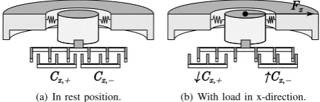
The sensor consists of a suspended core which is fabricated in the handle layer of an SOI wafer. The suspended core is supported by v-shaped silicon springs. An applied load to the suspended core will result in a displacement. In-plane displacement caused by a shear force is measured by comb-structures present in the device layer and results in a differential change in gap between the comb-fingers (figure 2.9).
Cx,−
Cx,+
(a) In rest position.
Fx
↑Cx,−
↓Cx,+
(b) With load in x-direction.
Figure 2.9: Principle of operation for shear forces.
A normal force results in an out-of-plane displacement, which is measured by parallel plate electrodes (figure 2.10b). By differential measurement of two opposite electrodes (figure 2.10c), the applied torque is determined.
Cz,11 Cz,22
(a) In rest position.
Fz
↓Cz,11 ↓Cz,22
(b) With load in z-direction.
Tx
↑Cz,11 ↓Cz,22
(c) With torque around x-axis.
Figure 2.10: Principle of operation for normal forces and torques.
2.4.2
Mathematical model of the mechanics of the stage
All spring systems that are going to be used in the design of the sensor are bending beams. The Euler-Bernoulli beam theory is a cornerstone of mechanical engineering in the past century and covers the behavior of deflecting beams due to lateral loads.
Euler-Bernoulli beam theory
The Euler-Bernoulli beam equation describes the relationship between deflection and load [18]:
d2 dx2
EId
2u dx2
=q, (2.1)
withE Young’s modulus,I the second moment of area,uthe deflection,xthe horizontal coordinate of a point at the beam andqthe distributed load (as force per unit of length).
Young’s modulusEand the second moment of areaImay be assumed constant; equation 2.1 becomes:
EId 4u
2.4. MATHEMATICAL MODEL
The force is at the end L of the beam in one point. This can be defined by a Dirac delta function δ(x−L).
EId 4u
dx4 =F δ(x−L) (2.3)
Integration at both sides of the equation leads to a force atx=L in the right-hand side.
EId 3u dx3 =
ˆ
F δ(x−L) dx=F(L) +c1=F(L) (2.4)
It appears that the left-hand side of the equation is equal to the shear force. c1 will conflict when it is non-zero. A second integration leads to the bending moment.
EId 2u
dx2 =F(L)x+c2 (2.5)
And the third integration leads to the bending speed.
EIdu dx=
1
2F(L)x2+c2x+c3 (2.6)
The fourth integration leads to an equation with the actual deflection.
EIu=1 6F(L)x
3+1
2c2x2+c3x+c4 (2.7)
The integration constantsc2, c3 andc4 vary for different boundary settings and can be found using equations 2.5, 2.6 and 2.7. Substituting the integration constants in 2.7 leads to a the right beam model.
Two beam models are derived: a beam with a guided end and a beam with a free end.
Boundary conditions for a beam with a guided end
A guided beam is fixed at one end and is guided at the other end. A point force is applied at the guided end. Figure 2.11 shows a guided beam with the dimensions.
F u L
x
Figure 2.11: Guided beam with dimensions.
The beam is fixed atx= 0.
u|x=0= 0→c4= 0 (2.8)
du dx x=0= 0
→c3= 0 (2.9)
Half of the total bending moment is atx=L, this models the guided end of the beam.
M = −EId 2u dx2 x=L=
1
2F(L)L→c2=−1
2F(L)L (2.10)
Substituting the boundary conditions leads to the following equation.
EIu= 1 6F(L)x
3
−1
4F(L)Lx
2 (2.11)
Rewriting the equation results in a model for a guided beam.
u=−F(L)x
2
12EI (3L−2x) (2.12)
The result corresponds with [31]. The deflection at the end of the beam (x=L) is:
u=−F L
3
PART 2. THEORY
F u L
x
Figure 2.12: Beam with free end with the dimensions.
Boundary conditions for a beam with a free end
A beam with a free end is fixed at one end and is free at the other end. A point force is applied at the free end. Figure 2.12 shows a beam with a free end with the dimensions.
The beam is fixed at x= 0.
u|x=0= 0→c4= 0 (2.14)
du dx x=0= 0
→c3= 0 (2.15)
The total bending moment is at x= 0, since this is the only location where it is has constraints.
M = −EId 2u dx2 x=0=
F(L)L→c2=−F(L)L (2.16)
Substituting the boundary conditions leads to the following equation.
EIu= 1
6F(L)x3− 1
2F(L)Lx2 (2.17)
Rewriting the equation results in a model for a guided beam.
u=−F(L)x
2
6EI (3L−x) (2.18)
The result corresponds with [31]. The deflection at the end of the beam (x=L) is:
u=−F L
3
3EI. (2.19)
Stiffness of the suspended core
The chosen edge-supported stage uses v-shaped springs. Ideal springs obey Hooke’s law.
F =k·u, (2.20)
T =c·φ, (2.21)
with F the force,uthe displacement andk the stiffness,T the torque, c the rotational stiffness and φthe angle. The system of springs is dimensioned for forces in the first place, therefore, it is necessary to know the stiffness in each direction. The chosen concept uses the point symmetric v-shaped spring system shown in figure 2.13.
2.4. MATHEMATICAL MODEL
L W
L
N3s
Figure 2.14: Handle layer with the point symmetric v-shaped spring system and the parameters of each spring.
However, the spring system is applied multiple times to achieve higher stiffnesses in all directions. Figure 2.14 shows the dimensions of the suspended core.
The stiffness in normal direction of a guided beam, consisting of two serial beams with lengthL, is:
kz= F uz =
12EI
(2L)3. (2.22)
As long as the suspended core is supported by flexures located in a point symmetrically way around the core, the stiffness of the is equal toN timeskz. Since the suspended core is supported by multiples of three flexures,N3s= 3N is the number of flexure triplets and is substituted in equation 2.23.
kstage,z = F uz =
36N3sEI
8L3 (2.23)
The stiffness matrix in both shear directions and the torsional stiffness can be obtained by using the free end beam theory in the way it was done in reference [34].
Kxyφ=
15EI
2L3 − 9EI 2L3 −
9EI 2L3 −9EI 2L3 15EI 2L3 3EI 2L3 −9EI 2L3 3EI 2L3 7EI 2L3 (2.24)
To obtain the stiffness in shear direction of the suspended core consisting of folded sheet flexures located point symmetrically, a displacement vector is defined in shear direction.
~
u=1 0 0 (2.25)
This vector can be rotatedφdegrees with rotation matrixHrot(φ).
Hrot(φ) =
cos(φ) −sin(φ) 0 sin(φ) cos(φ) 0
0 0 1
(2.26)
If there are three flexures, all 120◦ rotated with respect to each other, the stiffness in shear direction can be calculated by rotating the shear force vector 0◦, 120◦ and 240◦ and multiply each rotated vector with the stiffness matrix. Multiplying with the inverse of each rotated vector and calculating the sum of these result in the stiffness in shear direction. Summarized:
kx= 2 X i=0 ~ uHrot 2 3πi
k·~u−1= 45EI
2L3 . (2.27)
This corresponds to reference [34]. As long as the suspended core is supported by a point symmetric spring setup, the stiffness is equal in all shear directions. Equation 2.27 can be extended with supported for multiple flexure tripletsN3s.
kstage,x=
45N3sEI
2L3 (2.28)
The second moments of area are as follows.
Ix= T W3
12 , (2.29)
I = W T 3
PART 2. THEORY
withT the thickness of the beam (equal to the thickness of the handle layer) andW the width of the beam.
The six degrees of freedom mesa can be tuned for translations with parameters L, W and N3s by substituting the equations of 2.31 in equations 2.28 and 2.23:
kx∝ N3s
L3 W
3, (2.31)
kz∝ N3s
L3 W. (2.32)
The stiffness in x-direction compared to z-direction can be optimized by choosing the right value for the flexure width W, the stiffness in both directions can be tuned by the flexure part lengthL. When stiff structures are desired, the flexure part length L may be very small compared to the flexure width W. This may jeopardize the validity of mentioned model. Adding multiple spring tripletsN3sallows the flexure part lengthLto be larger. This results in an overconstrained construction, but it is not expected that this will introduce problems since the whole structure will be of a monolithic material.
2.4.3
Mathematical model of the electrostatics of the sensing structures
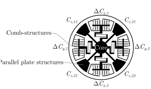
The sensor uses capacitive sensing structures. Figure 2.15 shows where the chosen capacitor structures are located.ΔCx,1
ΔCx,2
ΔCy,2
ΔCy,1
Cz,11 Cz,21
Cz,21 Cz,22
Comb-structures
Core
Parallel plate structures
Figure 2.15: Design of the device layer with declaration of all sensing capacitors.
There are large parallel electrode capacitors for normal force and torque measurements and comb-structures for shear force measurements. Both capacitor comb-structures can be modeled as gap closing parallel plate capacitors [14].
E A
d
a
b
Figure 2.16: A parallel plate capacitor with very large overlapping area compared to the distance between the plates.
The derivation for this capacitor is based on one of the Maxwell’s equations, i.e. Gauss’ law.
∇ ·E~ = ρ
ε (2.33)
In integral form and assuming uniform charge, this equation becomes:
‹
S ~
E·d~a=q
ε. (2.34)
For large overlapping plates, the integral can be solved in the following way:
‹
S ~
E·d~a=EA= q
ε →q=εEA. (2.35)
WithE the electric field normal to the surface. The capacitance is defined as:
2.4. MATHEMATICAL MODEL
And voltage between plateaand plate bis defined as:
u= ∆V =
ˆ b
a ~
E·d~l=Ed (2.37)
Substitution of 2.35 and 2.37 in 2.36 results in:
C=εA
d. (2.38)
For multiple parallel plates with equal area, e.g. comb fingers, it may be convenient to add a number of plate pairsNpto the equation.
C=Npε A d0−u
. (2.39)
Substituing Hooke’s law results in the following equation.
C(F) =Npε kA kd0−F
. (2.40)
Normal forces are measured non-differentially using the parallel plate capacitor structures. For small forces, the closing gap capacitor model can be linearized using the Maclaurin series:
Cz(Fz)≈ 1 X
n=0
Cz(n)(Fz) n! F
n z =
Np,zAz d2
0,zkz
Fz+Cz(0). (2.41)
All parameters can be put in factorβz:
Cz(Fz)≈βzFz+Cz(0), with βz=
Np,zAz d2
0,zkz
. (2.42)
C(F) is an expression for the total capacitance between two plates or two combs. As can be seen in the sensing structures in figure 2.15 and in the operating principles in figure 2.9 and 2.10, shear forces are measured differentially. The differential capacitance ∆Cxis defined as:
Cx,± =Cx,rest±Cx→∆Cx=
Cx,+−Cx,−
2 , (2.43)
i.e. the actual difference in capacitance due to displacement of one side, which can be measured by calculating half of the difference of the two measured structures (i.e. two plates or two combs). For small forces, the differential closing gap capacitor model may be linearized using the Maclaurin series:
Cx(Fx)≈ 1 X
n=0
∆Cx(n)(Fx) n! F
n
x (2.44)
=βxFx, with βx=
Np,xAx d2
0,xkx
. (2.45)
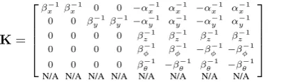
The invertedβ-factors are elements of calibration matrixK, which maps the measured capacitances (corresponding to the defined capacitances in figure 2.15) to forces and torques.
Fx Fy Fz Tx Ty Tz =K
∆Cx,1 ∆Cx,2 ∆Cy,1 ∆Cy,2 Cz,11 Cz,12 Cz,21 Cz,22
, with K∈R6×8 (2.46)
PART 2. THEORY
2.5
Design of the suspended core
The details of the design of the suspended core are described in this section.
2.5.1
Computer aided design
The suspended core with v-shaped springs is drawn in the CAD software SolidWorks Professional 2012 SP1.0. The circular core has a diameter of 2.5 mm. All v-shaped springs are point symmetrically oriented around the center of the core and consist of two beams with a length of 480 µm and a width of 108 µm.
The structures in the handle layer have rounded corners. This is done for two reasons:
• it reduces the maximum stress because the beams are thicker at places where the deformation would
be originally higher;
• the etching process does not allow very sharp corners. By using round corners in the simulations,
the simulations become more true to nature.
A 2D-top drawing is exported to the CleWin 5.0.13 Layout Editor. The stage is extended with a hexagon structure around it and two fixation points on both sides. Chapter 3 will go into more detail about this.
All parameters and the calculated stiffnesses are available in table 2.2.
Table 2.2: Dimensions of the suspended core.
Quantity Symbol Value
Length of one spring part L 480 µm
Width of the spring W 108 µm
Thickness of the spring T 400 µm Number of spring triplets N3s 5 Diameter of the core Dcore 2.5 mm Diameter of the sensor Dsensor 9.24 mm Stiffness in shear direction kx 7.2·106N m−1 Stiffness in normal direction kz 1.9·107N m−1
2.5.2
Stiffness and stress simulations
Two types of simulations were done. First, the sensor is simulated as if it is mounted on a very stiff supporting ring. This is done as verification of the mathematical model. Then, the sensor is simulated in a more realistic situation. The latter simulations are done to get an impression how the sensor will perform in the real world.
Ideally mounted
The simulations were done for a shear force of 10 N, a normal force of 10 N and a torque around a shear axis of 10 N mm. Table 2.3 shows the simulation results.
Table 2.3: FEM simulation results.
Quantity Symbol Value
Stiffness in shear direction kx 8.9·10−6N m−1 Maximum stress forFx= 10 N σmax,x 8.5 GPa Stiffness in normal direction kz 1.2·10−7N m−1 Maximum stress forFz= 10 N σmax,z 4.0 GPa Rotational stiffness around shear axes cx 41 N m rad−1 Maximum stress forTx= 10 N mm σmax,φ 0.92 GPa
2.5. DESIGN OF THE SUSPENDED CORE
Realistically mounted
The handle layer of the sensor is supported by a solid ring like is illustrated in figure 2.17. The material was unknown in the simulation phase and can vary between a plastic (∼4 GPa) and a ceramic (∼400 GPa).
Polysilicon (169 GPa) was used in these simulations. The ring has a thickness of 500 µm, the suspended core has a thickness of 380 µm. Latter property dates back to when it was assumed that SOI-wafers with a handle layer of 380 µm were going to be used.
Figure 2.17 shows the boundary conditions of the FEM simulation. The marked boundaries in figure 2.17a are fixed boundaries. The marked boundaries in figure 2.17b are loaded. By applying the loads in opposite shear direction at latter boundaries, a torque can be simulated.
(a) Fixed boundaries. (b) Force boundaries.
Figure 2.17: The model with boundary conditions.
The stiffness may be influenced by the supporting ring on top of the handle layer. Figure 2.18 shows the deformation of a section of the sensor with scale factor of 1000.
It appears that the support’s influence is negligible for shear forces. For normal forces, the compliance is for 0.77 % the consequent of the v-shaped springs. For torques, this is 0.81 %. It turns out that it is important to support the sensor with a stiff material, a ceramic printed circuit board (PCB) may be used for example.
The v-shaped springs have optimized shapes for stress distribution. The performance of this optimization is analyzed using figure 2.19a for shear forces, figure 2.19b for normal forces and figure 2.19c for torques. The v-shaped springs build up high stresses in the corners when loaded in the direction the v-shape points (figure 2.19a). In the other direction, the stress is minimal. In normal direction, the stress is especially consentrated at the corners (figure 2.19b), uniformly for all springs. The stress distribution for torques is almost the same as for shear forces (figure 2.19c).
The exact maximum stress before damage is not determined, for this is dependent of the direction. 10 N and 10 N mm are estimated as the maximum force and torque respectively.
2.5.3
Alternative designs
PART 2. THEORY
(a) Shear force of 10 N.
(b) Normal force of 10 N.
(c) Torque of 10 N mm.
Figure 2.18: Deformation analysis using FEM.
(a) Shear force of 10 N. At the top of the handle layer.
(b) Normal force of 10 N. Section in the middle of the handle layer.
(c) Torque of 10 N mm. At the top of the handle layer
Figure 2.19: Stress analysis using FEM for a shear force of 10 N pointed to the right.
Table 2.4: Three different spring systems for the suspended core.
Number of spring tripletsN3s Shear stiffness Normal stiffness Spring part lengthL Spring widthW
1 0.83 N µm−1 1.5 N µm−1 470 µm 84 µm
5 8.3 N µm−1 7.6 N µm−1 480 µm 108 µm
2.6. DESIGN OF THE SENSING STRUCTURES
2.6
Design of the sensing structures
The details of the design of the sensing structures are described in this section.
2.6.1
Computer aided design
The device layer with the sensing structures are drawn using the same software as the handle layer. SolidWorks was used to draw most parts of the device layer, including the comb-structures and the bond pads. The parallel plate structures were scripted and drawn in CleWin.
2.6.2
Comb-structures in the device layer
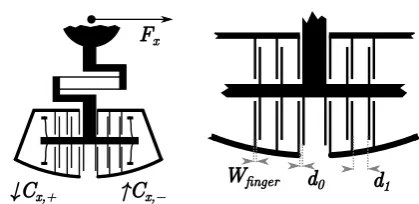
The comb-structures consist of two parts: the transmission from the mesa to the combs (the discriminating spring) and the finger-structures.
Discriminating spring and overload protection
The comb-structures consist of combs mounted on a one degree of freedom stage which is supported by eight single flexures. Spring and lever structures are used to seperate the different force components of the mesa into comb-structure movements (figure 2.20).
u
xu
x4
1
2
3
3
(a) Shear force in x-direction.
u
y4
1
2
3
3
(b) Shear force in y-direction.
u
z4
1
2
3
3
(c) Normal force in z-direction.
Figure 2.20: Transmission (2) from mesa (1) to comb-structures (4). There are bumps (3) to prevent snapping of the fingers due to overloading.
This spring system was modeled using equations 2.13 in MATLAB R2012b 8.0.0.783 and verified by simplified FEM simulation. The transmission has (for small displacements) very high stiffness in x-direction and therefore transfers the full x-displacement from the mesa to the comb-structures. In z-direction, the stiffness of the transmission springs are more than 80 times lower than the springs of the comb-structures, so less than 2 % of the z-displacement of the mesa is transferred to the comb-structures. In y-direction, the stiffness of the transmission springs are negligible compared to the the springs of the comb-structures making the comb-structures almost insensitive for y-displacements. In this way, crosstalk between the different force components is mechanically minimized.
All comb-structures have protection against snapping due to overloading: the stage will hit the bumps in figure 2.20 first before the fingers of the stage will snap to the fingers of the stator, as the distance between the finger pairs is 7 µm and the distance between the bumps and the stage is 5 µm.
Finger optimization
The shear displacements are measured differentially. The stator consists of two symmetric electrically isolated parts (figure 2.21). Displacement of the stage results in an increasing gap at one half of the comb-structures and a decreasing gap at the other half of the comb-structures.
The asymmetric positioning (d1/d0-ratio in figure 2.24b) of the shuttle-fingers between the stator-fingers is optimized, for a smaller d1/d0-ratio allows more finger structures but increases the parasitic capacitance and a largerd1/d0-ratio decreases the parasitic capacitance but takes more space. The curve in figure 2.22 is derived from equation 2.40, its maximum is where:
∂ ∂d1
1
d0+d1+ 2Wf inger 1
d0
− 1
d1
PART 2. THEORY
↓Cx+ ↑Cx− Fx
(a) Differential capacitance change when loaded.
Wfinger d0 d1
(b) Close-up of the finger structures with dimensions.
Figure 2.21: Electrical design of the comb-structures.
The fingers have a widthWf inger of 7 µm. The minimum distance between the fingers is 7 µm which is used for d0. Choosing ∼ 20 µm for d1 leads to maximum capacitance change. All parameters are summarized in table 2.5.
6e+08 8e+08 1e+09 1.2e+09 1.4e+09 1.6e+09 1.8e+09 2e+09 2.2e+09 2.4e+09
10 15 20 25 30 35 40 45 50
Factor
that
leads
to
higher
capacitance
Distanced1 [µm]
Figure 2.22: Optimization of the finger distances: choosingd0 the maximum of the function will conse-quent in the highest capacitance.
Table 2.5: Parameters of the comb-structures.
Quantity Symbol Value
Number of finger pairs Np, x 149
Average overlapping area per finger pair Ax 1.2·10−8m2
Distance between fingers d0 7 µm
Distance between finger pairs d1 20 µm
Width of a finger Wf inger 7 µm
Average length of a finger Lf inger 240 µm
Thickness of a finger Tdevice 50 µm
2.6.3
Parallel plate structures in the device layer
The parallel plate structures consist of flat plates that form a capacitor with the handle layer. The surface area of the plates is such that the capacitance is in the same order as the capacitance of the comb-structures.
Electrical connections