Abstract—The characteristics of Static Synchronous Series Compensator (SSSC) based on six-pulse Voltage Source Converter (VSC), which is inserted in series into a three phase inductive system, are analyzed and calculated in detail in its inductive and capacitive operation modes, including the AC, DC current and DC capacitor voltage in one period. And the expressions for them are derived in order to assess the compensator performance. The SSSC based on six-pulse VSC is specially studied because it gives an insight into the study of the more complex configurations. On the basis of calculations and simulations in PSCAD/EMTDC, the impact of current on DC capacitor charge and discharge is analyzed thoroughly. A methodology for the capacitor voltage control of SSSC is obtained. Meanwhile, a basis for choosing semiconductor devices of SSSC is presented in the paper.
Index Terms—control mechanism, impact of current on the capacitor, multi-pulse VSC, Static Synchronous Series Compensator (SSSC), Voltage Source Converter (VSC).
I. INTRODUCTION
Static Synchronous Series Compensator (SSSC) is a series type of Flexible AC Transmission System (FACTS) devices, which is based on self commutated converters formed by semiconductor switches with self turn-off capability. The main objective of the SSSC is the compensation of transmission lines. This device is inserted in series with the line to inject a voltage in quadrature with the line current in order to emulate a reactance. So it has a direct effect over the line current [1-2].
Voltage Source Converter (VSC) is the most crucial part of SSSC [3]. VSC has many types of topology configuration. The multi-pulse configuration is chosen in this paper due to its characteristics and applicability. Most of the existing VSC based FACTS devices rated above 80 MVAR use either 24 or 48-pulse converters [4], because they exhibit several advantages over other VSC configurations, e.g., better harmonic property, lower switching frequency, lower rated
This work was supported by the National Basic Research Program of the People’s Republic of China (973 Program) under Grant 2004CB217907.
Guanjun Ding is with the Department of Electrical Engineering, Hefei University of Technology. He is now studying in China Electric Power Research Institute, Beijing, 100192 P. R. China (phone: 13810818695; fax: 010-62913127; e-mail: [email protected]).
Guangfu Tang is with the Power Electronics Applying Technique Institute, China Electric Power Research Institute, Beijing, 100192 P.R. China (e-mail: [email protected]).
Ming Ding is with the Department of Electrical Engineering, Hefei University of Technology, Hefei, 230009 P. R. China (e-mail: [email protected]).
voltage level of DC capacitor, etc [5].
SSSC based on multi-pulse VSC has been researched in the past few years by some well-known scholars. For instance, Kalyan K. Sen researched on the SSSC based on 24-pulse VSC [6], and L. Sunil Kumar, Arindam Ghosh studied on the SSSC based on 48-pulse VSC [7]. But they didn’t analyze the AC and DC current of VSC and the impact of current on DC capacitor charge and discharge. These aspects are important because such analyses lead to full understanding of the converter and its mechanism for controlling and implementing it. And this is exactly the aim of the paper.
II. CHARACTERISTICS OF SSSC BASED ON SIX-PULSE VSC, ONLY REACTIVE POWER EXCHANGE
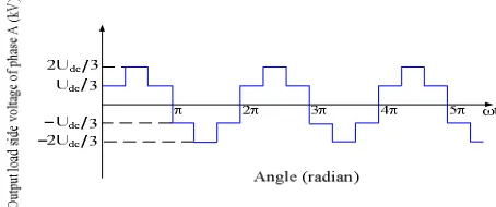
[image:1.595.312.539.461.556.2]The basic topology of VSC is six-pulse configuration, when the gate pulse pattern of its devices is fundamental switching mode, the output load side voltage of phase A is shown as Fig. 1.
Fig. 1. Output load side voltage of phase A of six-pulse VSC.
The transmission line impedance has resistive and inductive components, is mostly inductive. And it is such inductive component that the SSSC attempts to modify by injecting a voltage with controllable magnitude. So in the following, a three phase inductive system with pure inductive line is used to perform the analyses, in which SSSC based on six-pulse VSC is inserted in series representing a sinusoidal voltage source, shown as Fig. 2. The analyses include the AC, DC current and DC capacitor voltage of the VSC, and the impact of current on DC capacitor charge and discharge. The SSSC based on six-pulse VSC is specially studied because it gives an insight into the study of the more complex configurations.
Research on the Control Mechanism of DC
Capacitor Voltage of SSSC Based on Multi-pulse
VSC
Fig. 2. SSSC embedded in an inductive circuit.
In Fig. 2, the AC system voltage is “u=Um⋅sin
( )
ωt ”, the current i lags the voltage u by 90° due to the pure inductive line. “uSSSC” denotes the injected voltage with controllable [image:2.595.312.551.305.555.2]magnitude of SSSC. In real circuits it is a common practice to connect a star-star transformer with a turn ratio of 1:1 to the VSC in order to couple the VSC with an external circuit. The AC voltages are taken from the secondary side of the coupling transformer. Neglecting losses the current flowing in the secondary side equals the current in the primary side of each single phase transformer. Therefore the SSSC currents are the line currents. The vector diagram of voltages and current in inductive and capacitive operation modes of SSSC is shown in Fig. 3.
Fig. 3. Vector diagram of voltages and current.
In Fig. 3, uSSSC( )L denotes the injected voltage in inductive
operation mode of SSSC; uSSSC( )C denotes the injected
[image:2.595.101.237.318.417.2]voltage in capacitor operation mode of SSSC.
Fig. 4 depicts the AC system voltage u and the injected voltage uSSSC of phase A in one period.
Fig. 4. AC system voltage u and injected voltage uSSSC of phase A in one
period.
A. Analysis of AC side Current
The expression that describes the circuit shown in Fig. 2 is as (1), i.e., the current flowing between SSSC and the AC system is determined by the voltage across the inductor L.
( )
SSSCL t Ldtdi u u
u = = − (1) Taking into account the injected voltage uSSSC over each 60° conduction interval (see Fig. 4), the equation that describes the AC side current ia
( )
t is derived. The specific analysis is as follows:1) Interval: 0≤ωt≤π 3
( )
= ⋅( ) ( )
− − ⇒ 3 1S dcm
a U sinωt U
dt t di L
( )
=∫
( )
−∫
( )
− + 0 ⇒ 00 1 3L dt I
U dt
t
ω
sin L U t
i t m t S dc
a
( )
[
( )
]
( )
03 1
1 t I
L U t
ω
cos L
ω
U t
i m S dc
a = − − − ⋅ + (2)
where I0 is the initial condition at t=0, i.e., I0=ia
( )
0 . S isa marked sign, if SSSC is in its inductive operation mode, the value of S is zero, i.e., S=0; if SSSC is in its capacitive operation mode, the value of S is one, i.e., S=1. In the following expressions, S has the same meaning as abovementioned.
2) Interval: π 3≤ωt≤2π3
( )
= ⋅( ) ( )
− − ⇒ 3 2 1S dcm
a U sinωt U
dt t di L
( )
=∫
( )
−∫
( )
− + 1 ⇒3
3 3
2
1 dt I
L U dt
t
ω
sin L U t
i t
ω
π S dc
t
ω
π m
a
( )
t UωL 21 cos( ) ( )
ωt 1 2U3L t 3πω I1ia m S dc +
−
− −
−
= (3)
where
=i πω I1 a 3 .
3) Interval: 2π 3≤ωt≤π
( )
=( ) ( )
− − ⇒dc S m
a U sinωt U
dt t di L
3 1 1
( )
=∫
( )
−∫
( )
− + 2 ⇒3 2 3
2 3
1
1 U dt I
L dt
t
ω
sin L U t
i t dc
ω π
S t
ω
π m
a
( )
( ) ( )
3 22 3
1 1 2
1
I
ω π
t U L t
ω
cos L
ω
U t
ia m S dc +
− ⋅ −
−
− −
= (4)
where
=
ω π
i I a
3 2
2 .
It is known that in steady state the AC current waveform is symmetric, therefore,
0 2 =
ω π
ia (5)
taking into account the above property, I0, I1 and I2 can be calculated as (6).
( )
( )
( )
− −
=
+ −
=
− −
=
+
L
ω
U U L
ω π
I
L
ω
U U L
ω π
I
L
ω
U U L
ω π
I
m dc S
m dc S
m dc S
9 2 1
2 9
1
2 9
1
0
1 2
1
(6)
[image:2.595.53.289.537.667.2]( )
( ) ( )
( ) ( )
( ) ( )
≤ ≤ ⋅ − ⋅ − − − ≤ ≤ ⋅ − ⋅ − − − ≤ ≤ ⋅ − ⋅ − − − = π t ω π U L ω π L t t ω cos L ω U π t ω π U L ω π L t t ω cos L ω U π ω U L ω π L t t ω cos L ω U t i dc S m dc S m dc S m a 3 2 9 3 1 3 2 3 3 3 2 1 3 t 0 9 2 3 1 (7)Over the interval π≤ωt≤2π, the waveform of AC side phase current ia
( )
t is the negative respect to that described in (7). The other two phase currents, ib( )
t and ic( )
t are identical except phase shifted by 120° and 240° from ia( )
t , respectively.B. Analysis of DC Capacitor Current
Once the SSSC currents are known it is possible to derive the DC capacitor current idc. The DC capacitor current is constructed by adding segments of AC phase currents. The segments depend on which transistor-diode (G−D) pair is conducting. Analyzing the upper G−D pairs of the six-pulse VSC, it is observed that the pairs G1−D1, G3− D3 and
5
G −D5 participate in the DC capacitor current, thus,
c b a
dc gs i gs i gs i
i = 1⋅ + 3⋅ + 5⋅ (8)
where gs1, gs3 and gs5 are the gate signals of G1, G3 and 5
G respectively, and take values of 0 and 1 when they are off
and on respectively.
When the gate signal is present in the transistor of a upper
G−D pair, the transistor conducts if the current is negative and the diode conducts if the current is positive. Analyzing the gate pulse patterns of gs1, gs3 and gs5, the following behavior of idc can be deducted for a cycle in the inductive
mode of operation. For the capacitive operating mode, the intervals are the same except that are phase shifted by 180°.
1) Interval: 0≤ωt<π 3
Signals gs1 and gs5 are activated, therefore idc is formed
of ia and ic, i.e.,
( )
t i( ) ( )
t i tidc = a + c (9)
where c
( )
m UdcL ω π t L π t ω cos L ω U t
i ⋅
⋅ + − + − = 9 3 1 3 2 . 2) Interval: π 3≤ωt<2π3
Only gs1 is present, consequently idc equals ia, i.e.,
( )
t i( )
tidc = a (10) 3) Interval: 2π 3≤ωt≤π
Signals gs1 and gs3 are activated, thus idc is constructed
of ia and ib, i.e.,
( )
t i( ) ( )
t i tidc = a + b (11)
where b
( )
m UdcL ω π t L π t ω cos L ω U t
i ⋅
⋅ − − − − = 9 4 3 1 3 2 . Taken together abovementioned and in combination with (7), the expression for DC capacitor current idc
( )
t is as follows.( )
( )
( )
( )
≤ ≤ ⋅ − − + − ≤ <⋅ − − − − < ≤ ⋅ − − − − =
+ U π ωt π
L ω π L t π t ω sin L ω U π t ω π U L ω π L t π t ω sin L ω U π t ω U L ω π L t π t ω sin L ω U t i dc m S dc m S dc m S dc 3 2 9 5 3 2 6 1 3 2 3 3 3 2 2 1 3 0 9 3 2 6 1 1 (12)
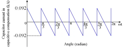
These expressions are equivalent except phase shifted by 60° among them; therefore the capacitor current waveform over each of the remaining three conduction periods is identical to that described by (12), and yields, in a repetitive waveform, six times the corresponding AC system frequency. When the parameters used are Um=220 2 V, L=6mH,
[image:3.595.314.550.52.146.2]f=50Hz and Udc =50V, the waveforms of idc
( )
t in the inductive operation mode and capacitive operation mode of SSSC are shown as Fig. 5 and 6, respectively.Fig. 5. DC capacitor current idc
( )
t in inductive operation mode of SSSC.Fig. 6. DC capacitor current idc
( )
t in capacitive operation mode of SSSC. As seen in Fig. 5 and 6, the capacitor current results in a periodic waveform with a period of 60°.C. Analysis of DC Capacitor Voltage
Assuming a lossless SSSC, the DC capacitor is initially charged and preserves its charge during the operation. The DC capacitor voltage is given by the following expression.
( )
( )
01 i tdt U C
t
udc =
∫
dc + (13) where U0 is the initial capacitor voltage, i.e., U0 =udc( )
0 .Assuming that the capacitor current remains significantly unchanged from that given by (12), the DC capacitor voltage can be estimated; under this condition a minimum DC ripple voltage is obtained [8]. The capacitor voltage over the first 60° period is given by:
( )
( )
00
1 i tdt U C
t
udc =
∫
tdc + (14) where t∈[0, T], andω π
T 3
= .
[image:3.595.309.545.404.497.2]( )
tudc can be obtained and shown as (15).
( ) ( )
−
− −
⋅ − =
6 2
3
1 2 cos ωt π
LC
ω
U t
u S m
dc
0 2
9
3 ωLCU t U
π
t LC U
dc
dc + ⋅ + (15)
At the same time the DC voltage level Udc =T
∫
Tudc( )
tdt0
1 ,
so the value of U0 can be calculated and shown as (16).
( )
S m dc UdcLC
ω
U .
LC
ω
U .
U = − ⋅ ⋅ − +
2 2
0 1 0089 006097 (16)
So (15) can be transformed into (17), it’s the expression for
( )
tudc .
( ) ( )
− +
−
− ⋅
−
= 2
2 0955 6 3
1 t
LC U
π
t
ω
cos . LC
ω
U t
u S m dc
dc
dc dc
dc U
LC
ω
U .
t U LC
ω π
+ −
⋅ 006097 2
9 (17)
From the relationship between udc
( )
t and idc( )
t , i.e., (13) or (14), it is known that when idc( )
t has the value of zero,( )
tudc has extremum value Upk of capacitor voltage shown
as follows.
( )
S m dc dcdc
pk U
LC
ω
U . LC
ω
U .
ω π
u
U = − ⋅ + +
= +
2 2
1 0045 00304 1
6 (18)
If SSSC is in its inductive operation mode, Upk is the
minimum value; if SSSC is in its capacitive operation mode,
pk
U is the maximum value. So there are two quantities are worth attention, i.e., the initial capacitor voltage in inductive operation mode (denoted as U0L) and Upk in capacitive
operation mode (denoted as UpkC ). Taking higher value
between U0L and UpkC, and this higher value is denoted as max
U , i.e., Umax =max
(
U0L,UpkC)
. Comparing correspondingexpressions of U0L in (16) and UpkC in (18), the following
can be got that if Udc≤0.482Um , Umax =U0L; if Udc ≥ m
U .482
0 , Umax =UpkC . Umax is very important to
semiconductor devices because the capacitor voltage is applied directly to the semiconductor devices, therefore those semiconductor devices must be able to support that voltage. And it is a basis for choosing semiconductor devices of SSSC.
The abovementioned parameters are still used, and
C=500µF, then the waveforms of udc
( )
t in the inductive operation mode and capacitive operation mode of SSSC are shown as Fig. 7 and 8, respectively. [image:4.595.44.294.51.434.2]Fig. 7. DC capacitor voltage udc
( )
t in inductive operation mode of SSSC.Fig. 8. DC capacitor voltage udc
( )
t in capacitive operation mode of SSSC.The DC capacitor current described as (12) and shown in Fig. 5 and 6 has an average value of zero. Thus, taking into account (13), the capacitor current does not have effect on the capacitor charge regardless the type of compensation the SSSC is providing. That is, when the compensator voltage is in quadrature with the line current only reactive power is exchanged between the compensator and the system. Otherwise, a different behavior is found. To show this, a phase shift in u is considered, i.e., u=Um sin
(
ωt−θ)
. The specific analyses are as follows.III. CHARACTERISTICS OF SSSC BASED ON SIX-PULSE VSC,
BOTH REAL POWER AND REACTIVE POWER EXCHANGE
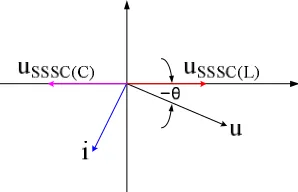
[image:4.595.310.542.51.138.2] [image:4.595.352.501.430.526.2]A phase shift θ is considered in u, i.e., u=Umsin
(
ωt−θ)
. The vector diagram of voltages and current in inductive and capacitive operation modes of SSSC in this case is shown in Fig. 9. Fig. 10 depicts the AC system voltage u and the injected voltage uSSSC of phase A in one period in this case. [image:4.595.311.541.565.683.2]Fig. 9. Vector diagram of voltages and current with θ>0.
Fig. 10. AC system voltage u with phase shift θ>0 and injected voltage
SSSC
u of phase A in one period.
A. Analysis of AC side Current
[image:4.595.54.285.655.741.2]in this case in steady state the AC current waveform has the following property.
( )
− = ω π iia0 a (19)
So I0, I1 and I2 can be calculated in this case. By means of calculations, the expression for ia
( )
t is described as (20) in this case.( )
(
) ( )
(
) ( )
(
) ( )
≤ ≤ − − − − − ≤ ≤ − − − − − ≤ ≤ − − − − − = π t ω π U L ω π L t θ t ω cos L ω U π t ω π U L ω π L t θ t ω cos L ω U π t ω U L ω π L t θ t ω cos L ω U t i dc S m dc S m dc S m a 3 2 9 3 1 3 2 3 3 3 2 1 3 0 9 2 3 1 (20)B. Analysis of DC Capacitor Current
A similar procedure to that presented in section Ⅱ.B is carried out. The expression for idc
( )
t is described as (21).( )
( )
( )
( )
≤ ≤ − − + − − < ≤ − − − − − < ≤ − − − − − =+ U π ωt π
L ω π L t π θ t ω sin L ω U π t ω π U L ω π L t π θ t ω sin L ω U π t ω U L ω π L t π θ t ω sin L ω U t i dc m S dc m S dc m S dc 3 2 9 5 3 2 6 1 3 2 3 3 3 2 2 1 3 0 9 3 2 6 1 1 (21)
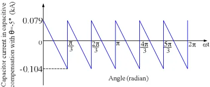
[image:5.595.322.533.62.150.2]The abovementioned parameters are still used, the waveforms of idc
( )
t in the inductive and capacitive operation mode of SSSC with θ=5°, θ=−1° and θ=−5° are shown as Fig. 11-14, respectively.Fig. 11. DC capacitor current (inductive compensation with θ=5°).
[image:5.595.348.504.248.342.2]Fig. 12. DC capacitor current (inductive compensation with θ=−1°).
Fig. 13. DC capacitor current (capacitive compensation with θ=5°).
Fig. 14. DC capacitor current (capacitive compensation with θ=−5°).
C. Analysis of DC Capacitor Voltage
The waveforms of udc
( )
t in the inductive and capacitive operation mode of SSSC with θ=−1°and θ=5° are shown as Fig. 15 and 16, respectively.0.06 0.07 0.08 0.09 0.10 0.11 0.12
-0.05 0.00 0.05 0.10 0.15 0.20 0.25 0.30 C ap ac ito r v olta ge in in du ctiv e co mp en sa ti on w ith θ =-1 ° (kV ) Time (S)
Fig. 15. DC capacitor voltage (inductive compensation with θ=−1°).
[image:5.595.50.291.296.395.2]0.065 0.070 0.075 0.080 0.085 0.090 0.095 0.100 -0.10 -0.05 0.00 0.05 0.10 0.15 0.20 0.25 0.30 0.35 0.40 0.45 0.50 Ca pa cito r v olta ge in c ap ac itiv e co m pen sat io n w ith θ =5 ° (k V ) Time (S)
Fig. 16. DC capacitor voltage (capacitive compensation with θ=5°).
IV. CONCLUSION
The theoretical calculations and simulation results lead to the following three conclusions:
1) When the injected voltage of the SSSC is in quadrature with the line current, the capacitor current has an average value of zero. So the capacitor current doesn’t have effect on the capacitor charge regardless the type of compensation the SSSC is providing. Only reactive power is exchanged between the SSSC and the system. If the injected voltage leads the line current by 90°, it acts as a reactor, and it only absorbs reactive power. If the injected voltage lags the line current by 90°, it acts as a capacitor. Thus, it only provides reactive power. 2) When the injected voltage is out of quadrature with
[image:5.595.350.504.377.462.2] [image:5.595.64.274.452.538.2]absorbs reactive power while provides active power. 3) When the injected voltage is out of quadrature with the line current, if the voltage lags the current by an angle between 0° and 90°, the capacitor current has a positive average value, thus the capacitor will be charged. At this time, the SSSC acts as a capacitor reactance providing reactive power while absorbing active power. If the voltage lags the current by an angle greater than 90°, the capacitor current has a negative average value that discharges the capacitor, so the SSSC not only provides reactive power, but provides active power.
The degree of compensation of SSSC is proportional to the magnitude of the injected voltage, and, withal, the injected voltage is proportional to the DC capacitor voltage. With the above conclusions, a procedure to charge or discharge the capacitor can be easily applied. Therefore, the degree of compensation can be adjusted by charging or discharging the capacitor to the desired level easily. In addition, in practical circuits, VSC configurations are not losses, so the SSSC angle has to be varied a few degrees to be out of quadrature with the line current, enabling the flow of positive average capacitor current to compensate for the losses maintaining the desired capacitor voltage level.
REFERENCES
[1] N. G. Hingorani, "High Power Electronics and flexible AC Transmission System," IEEE Power Engineering Review, vol. 18, pp. 3-4, July 1988.
[2] N. G. Hingorani, and L. Gyugyi, Understanding FACTS: Concepts and Technology of Flexible AC Transmission Systems, vol. I. New York: IEEE Press, 2000, pp. 1-26.
[3] L. Gyugyi, C. D. Schauder, and K. K. Sen, "Static synchronous series compensator: a solid-state approach to the series compensation of transmission lines," IEEE Trans. Power Delivery, vol. 12, pp. 406-417, Jan. 1997.
[4] C. Schauder, M. Gernhardt, E. Stacey, T. Lemak, L.Gyugyi, T. W. Cease, and A. Edris, "Development of a ±100MVAR static condenser for voltage control of transmission systems," IEEE Trans. Power Delivery, vol. 10, pp. 1486-1493, July. 1995.
[5] D. Soto, and T. C. Green, "A comparison of high-power converter topologies for the implementation of FACTS controllers," IEEE Trans. Industrial Electronics, vol. 49, pp. 1072-1080, Oct. 2002.
[6] K. K. Sen, "SSSC-Static synchronous series compensator: theory, modeling and applications," IEEE Trans. Power Delivery, vol. 13, pp. 241-246, Jan. 1998.
[7] L. S. Kumar, and A. Ghosh, "Modeling and control design of a static synchronous series compensator," IEEE Trans. Power Delivery, vol. 14, pp. 1448-1453, Oct. 1999.