Abstract—For the scenarios with moderate data throughput and low area overhead, this paper designs a compact SM4 encryption and decryption algorithm circuit based on reusing the S-box in key schedule and round transformation. In addition, the area of proposed circuit could be further reduced by Composite Field Approach and optimizing the critical path of the circuit by dividing timing. Finally, the design of state machine that controls the encryption and decryption process is presented. Under the SMIC 0.18μm CMOS process, the synthesized circuit occupies only 0.057 mm2 of resources. Compared with other implementations, the proposed design has a higher ratio of throughput/gate, which is very suitable for low area overhead applications such as smart IC cards.
Index Terms—Encryption and decryption, SM4, Composite Field, reusing
I. INTRODUCTION
ITH the development of 5G and the Internet of Things (IoT), a large amount of information needs to be transmitted between the IoT terminals and the base station, which leads to the challenge of the security of the transmitted information. The SM4 algorithm is a block cipher algorithm issued by the National Cryptographic Authority of China and was identified as the national cryptographic industry standard in March 2012 [8]. With the rapid development of integrated circuit technology, the implementation of cryptographic algorithms using hardware circuits has received widespread attention. Compared with traditional software encryption methods, hardware encryption has the advantages of fast operation and high efficiency. Since the SM4 algorithm structure has the advantages of clear steps and easy hardware
Manuscript received July 17, 2019. This work was supported by the National Natural Science Foundation of China (No. 61774086), the Fundamental Research Funds for Central Universities (No. NP2019102, NS2017023), and the Natural Science Foundation of Jiangsu Province (No.BK20160806).
Xiangli Bu is with College of Electrical and Information Engineering, Nanjing University of Aeronautics and Astronautics (NUAA), Nanjing 210016, China (e-mail: [email protected]).
Ning Wu is with the College of Electronic and Information Engineering, Nanjing University of Aeronautics and Astronautics (NUAA), Nanjing 210016, China (e-mail: [email protected]).
Fang Zhou is with the College of Electronic and Information Engineering, Nanjing University of Aeronautics and Astronautics (NUAA), Nanjing 210016, China (e-mail: zfnuaa@ nuaa.edu.cn).
Muhammad Rehan Yahya is with the College of Electronic and Information Engineering, Nanjing University of Aeronautics and Astronautics (NUAA), Nanjing 210016, China (e-mail: [email protected]).
Fen Ge is with the College of Electronic and Information Engineering, Nanjing University of Aeronautics and Astronautics (NUAA), Nanjing 210016, China (e-mail: gefen@ nuaa.edu.cn).
implementation, it is of great significance to study the hardware circuit implementation of the SM4 algorithm.
Recently, lots of research have being done on the implementation of small-area SM4 algorithm circuits. Reusing the S-box in the encryption and decryption part to achieve the goal of reducing the area is proposed in [1]. However, it fails to fully optimize the circuit structure and reduce the critical path length of the circuit. Since the S-box is the only nonlinear operation in the SM4 algorithm [9], it acts on each round of encryption and decryption operations and key schedule, so the hardware implementation performance of the S-box largely determines the hardware implementation performance of the entire SM4 algorithm [10]. Such as circuit area, throughput and power consumption. In the hardware design process of the SM4 algorithm, the S-box is usually constructed by using the look up table (LUT) method, and the hardware implementation is simple, but the area overhead is large [11]. A technique for constructing an S-box based on a Composite Field Approach (CFA) is proposed in [2]. The S-box circuit implemented by CFA is not only easy to implement, but also has a much smaller area. Therefore, the inversion operation of the Finite Field GF(28) in the S-box can be mapped to the Composite Field GF((24) 2) to reduce circuit area overhead.
In this paper, based on the structure of reusing the S-box in key schedule and round transformation, we propose an optimization method to implement a compact SM4 encryption and decryption algorithm circuit. The S-box is implemented based on the CFA, and the critical path of the encryption and decryption circuit is optimized by dividing timing, thereby, implementing a small area SM4 circuit.
The rest of the paper is organized as follows: Section II introduces the overview of SM4 algorithm. Design of SM4 encryption and decryption circuit and their implementation are described in Section III. Section IV presents the performances and resource consumption of the design. Finally, the conclusions are drawn in Section V.
II. THE OVERVIEW OF SM4 ALGORITHM
Similar to the DES and AES algorithm, SM4 is a block cipher algorithm with 128-bits block length, and its key length also consists of 128 bits. Both the round transformation algorithm and the key schedule algorithm adopt a 32-round nonlinear iterative structure. The round transformation operation is performed in units of words (32 bits), and each iteration operation is a conversion function [6]. The SM4 encryption algorithm and decryption algorithm have the same structure except that the round key is reversed, wherein the decryption round key is the reverse order of the
A Compact Implementation of SM4 Encryption
and Decryption Circuit
Xiangli Bu, Ning Wu, Fang Zhou, Muhammad Rehan Yahya, Fen Ge
encryption round key (rki) [7]. Detailed key schedule algorithm and round transformation algorithm is shown as Algorithm 1 and 2 respectively.
As we can see from Algorithm 1, Key schedule generates
rki which is needed in the round transformation. In Algorithm 1 and 2, the “Ze
2” represents e-bit vector set and the “<<<”
represents a loop left shift operation. T´(·) in Algorithm 1 is a synthetic replacement and reversible. It is composed of a nonlinear transformation τ(·) and a linear transformation L´(·).
Round transformation in Algorithm 2 calculates the plaintext which uses 32 rounds round function Xi+4 = Xi⊕ T(Xi+1⊕Xi+2⊕Xi+3⊕rki). T(·) is also composed of a nonlinear transformation τ(·) and a linear transformation L(·). The Sbox in both Algorithm 1 and 2 is exactly the same, which is composed of a nonlinear operation with 8-bit input and output. It has been realized using CFA and discussed in Section III.
III. DESIGN AND IMPLEMENTATION OF SMALL AREA SM4
CIRCUIT
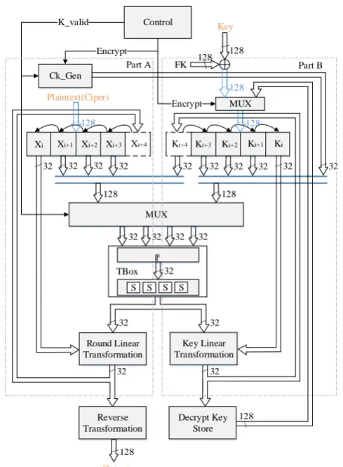
It can be observed from the structure of SM4 algorithm discussed in Section II, that there are identical S-boxes in key schedule and round transformation. Therefore, to realize compact SM4 encryption and decryption circuit, we first reduce the circuit by the overall structure of reusing S-box. Combined with the principle of SM4 algorithm, the overall block diagram of the SM4 encryption and decryption circuit shown in Fig. 1.
In Fig. 1, the Control module is used to control the operation of the entire encryption and decryption process. The Ck_Gen module is used to generate the parameters CKi,
required for key schedule. The designs of the Control and CK_Gen module are discussed in later part of this Section. The middle TBox reuses the same part of the round conversion and key schedule, and it consists of XOR gate and S-box. The Mux module is a multiplexer for selecting
whether the data entering the TBox is Round transformation data or Key schedule data. The Round Linear Transformation module and the Reverse Transformation module respectively refer to the linear transformation L(·) and the reverse transformation R(·) mentioned in Algorithm 2 in Section II. The Key Linear Transformation mod le refers to the Linear transformation L (·) mentioned in Algorithm 1. We can also see that the graph is divided into two parts by the curve box, where PartA is the round transformation part, and PartB is the key schedule part. As for why CK_Gen module is placed in the Round transformation section, it will be discussed below. Based on the structure shown in Fig. 1, we first optimize the S-box in the SM4 encryption and decryption circuit. The
Cki generation circuit is then optimized. Finally, the state machine that controls the timing is designed to implement a fully usable compact SM4 encryption and decryption circuit.
A. The optimization of S-box based on CFA
The area of the SM4 encryption and decryption circuit and the clock frequency largely depend on the implementation of its S-box. This is because S-box is non-linear and nonlinear operations require a lot of calculations. There are two ways to implement the S-box, one is to use a LUT, and the other is to use CFA. However, many studies have shown that a large number of hardware resources are required for use of the LUT method [2]. To reduce the area consumption, we chose the CFA technique to optimize the S-box.
The overall architecture of the S-box
The S-box operation of SM4 includes pre-affine operations, GF(28) inversion operations, and post-affine Algorithm 1 Key schedule
Input: key=(ZK0, ZK1, ZK2, ZK3), ZKi∈Z
32 2;
Use (K0, K1, K2, K3) = ( ZK0 ⊕ FK0, ZK1 ⊕ FK1, ZK2 ⊕ FK2, ZK3⊕ FK3) , Ki∈ Z
32 2;
Where FK3 = (B27022DC), FK2 = (677D9197), FK1 = (56AA3350), FK0 = (A3B1BAC6);
cki,j = (4i+j)×7(mod 256) (j=0,1,2,3;i=0,1,…,31); CKi = (cki,0, cki,1, cki,2, cki,3)∈( Z
8 2)4 ;
T´(·) = L´(τ(·));
C = (c0, c1, c2, c3)∈( Z
8 2)
4 ;
B = τ(C) = (Sbox(c0), Sbox(c1), Sbox(c2), Sbox(c3)) ∈( Z
8 2)4 ;
T´(C) = L´(B) = (B<<<23)⊕(B<<<13)⊕B;
Output: rki = Ki+4 = Ki ⊕T´(Ki+1⊕Ki+2⊕Ki+3⊕CKi) ∈ Z
32 2
(i=0,1,…,31);
Algorithm 2 Round transformation
Input: ciper=(X3, X2, X1, X0), Xi∈Z
32 2 ;
Xi+4 = Xi⊕T(Xi+1⊕Xi+2⊕Xi+3⊕rki);
T(·) = L(τ(·));
C = (c0, c1, c2, c3)∈( Z
8 2)
4 ;
B= τ(C) = (Sbox(c0), Sbox(c1), Sbox(c2), Sbox(c3)) ∈( Z
8 2)4 ;
T(C) = L(B)=(B<<<24)⊕(B<<<18)⊕(B<<<10)⊕(B<<<2)⊕B; Output: Y=R(X32, X33, X34, X35)=(X35, X34, X33, X32) ∈( Z
8 2)4;
Round Linear Transformation
Key Linear Transformation MUX
Xi Xi+1 Xi+2 Xi+3 Xi+4 Ki+4 Ki+3 Ki+2 Ki+1 Ki
32 32 32 32 32 32 32 32
128 128
32 32
32 32 32 32
32 32
Control
Ck_Gen
Reverse Transformation
\ 128
Output
32 32
Encrypt K_valid
Part A Part B
S S S S
\ 32
128 128
Plaintext(Ciper)
Decrypt Key Store
128 \
FK
\
Key
128 128
MUX
128
[image:2.595.307.552.51.384.2]TBox
operations, and the corresponding Finite Field operations are expressed as (1).
Y
T TX
C
1
C
(1) Where X and Y is the input and output of the S-box respectively. T and C represent the affine matrix of the SM4 S- box and the constants in the affine operation, respectively. Both T and C are constants and can be expressed as (2).1 1 0 1 0 0 1 1
1
1 1 1 0 1 0 0 1
1
1 1 1 1 0 1 0 0
0
0 1 1 1 1 0 1 0
1
=
,
0 0 1 1 1 1 0 1
0
1 0 0 1 1 1 1 0
0
0 1 0 0 1 1 1 1
1
1 0 1 0 0 1 1 1
1
T
C
(2)
Since the inversion operation in the Finite Field is very resource-intensive, studies have shown that mapping the inversion operation in the Finite Field to the Composite Field can greatly reduce the amount of computation. Using CFA technique, the following irreducible polynomial is used to decompose the multiplicative inverse operation (MIO) on the Finite Field into a Composite Field expressed as (3).
2
4 2
1
4 4 3 2
2
2
:
2
:
1
GF
f x
x
x
k
GF
f
y
y
y
y
y
(3)
Where k = {0010}2. Using CFA, the SM4 S-box can be
expressed as (4).
1 1
Y
T
TX
C
C
(4)Where δ–1=[0x3a, 0x52, 0xa5, 0xc5, 0x77, 0x2a, 0x26, 0x01]. To reduce hardware resource consumption, we combine matrix T and matrix δ-1 into a single matrix, i.e. M =
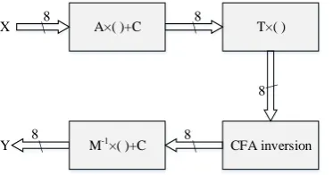
T × δ–1. According to (4), the new architecture of the S-box is shown in Fig. 2.
The implementation of the multiplicative inverse operation Over GF((24)2)
Let γ be a root of the irreducible polynomial f2(y)=0 in (3), then (γ, 1) forms the polynomial basis of the GF((24
)2). The polynomial basis expression of an element A in GF((24)2) can be represented as A=Ahγ+Al, wherein {Ah, Al}∈GF(24). Then, the polynomial inverse operation expression of the GF((24)2) based on the polynomial basis is derived by Finite Field operation expressed as (5).
1 2
1 2
h h h h l l
l h l h h l l
B
A
A
A
A A
B
B
A
A
A
A
A A
(5)
Where B = Bhγ + Bl. According to (5), we can get the circuit structure shown in Fig. 3. As it can be seen from Fig. 3, the MIO over GF((24)2) includes three multiplications, one square, one constant multiplication, one MIO, and two additions. These operations are all over GF(24). We can use bitwise XOR operations to replace the two additions. To reduce the number of gates, we implement the constant multiplication and square as one module.
Suppose a=a3ω3+a2ω2+a1ω+a0, b=d3ω3+ d2ω2+ d1ω+ d0 and c=c3ω3+c2ω2+c1ω+c0, they are all over GF(24).
According to the second irreducible polynomial in (3), the MIO a = b-1 can be expressed as (6), and the multiplication a =
b × c can be expressed as (7). S bstit ting ε= {0010}2 into (7),
we can see that the ()2×ε does not consume any hardware resources [5].
3 3 2 0 3 1 0 3 1 2 0 2 1 2 3 2 0 2 1 0 2 0 1 0 3 1
1 3 2 1 3 1 0 2 1 0 3 0 2 1 2 0 1 0 3 2 1 3 2 0 3 2 2 0 1 0
a b b b b b b b b b b b b a b b b b b b b b b b b b
a b b b b b b b b b b b b b b b b a b b b b b b b b b b b b
(6)
3 3 1 1 3 3 0 0 3 2 1 1 2 2 2 2 3 1 1 3 2 0 0 2 2 2 1 1 1 3 1 1 3 1 0 0 1 3 3 2 2 0 3 2 2 3 3 1 1 3 2 2 0 0
a b c b c b c b c b c b c b c a b c b c b c b c b c b c a b c b c b c b c b c b c a b c b c b c b c b c b c
(7)
As we can see from (6) and (7), there are still some redundant gates in the direct implementation. To reduce the
A×( )+C
X \ \ T×( )
CFA inversion
\
\ M-1×( )+C
Y \
8
8
8
8
[image:3.595.64.290.197.340.2]8
Fig. 2. the new architecture of the S-box
Ah 4
Al
()2×ε
()-1
Bh
Bl
4 4
4
[image:3.595.77.264.680.778.2]
hardware complexity, we use the DACSE algorithm [4] to optimize the multiplication on GF(24). After optimization, the circuit takes only 15 XORs and 16 ANDs, requiring 69 equivalent gates. Compared to direct implementation, the total resource consumption is reduced by 31%.
B. The optimization of Cki generation circuit
Using Algorithm 1, the formula for generating Cki parameters is shown in (8).
,
4
7 mod(256)
i j
ck
i
j
(8)The circuit can be implemented in two ways. One is to place the pre-generated parameters in the hardware circuit and use the multiplexer to select. Another way is to use the circuit to generate the current Cki parameters in order. The former method brings huge area overhead, but the generation of Cki is fast. The area occupied by the latter approach is much smaller than the former approach, but there is a circuit delay. Since we mainly focus area consumption, we use latter approach in our design.
According to the characteristics calculated by the hardware circuit, equation (8) can be converted into (9), which can reduce the area of the circuit. However, problem of critical path delay for circuit still exists.
,
2
3
i j
a
i
j
ck
a
a
(9)Since Cki parameter is required to generate the key, the round key conversion operation needs to input the current round key value. In theory, if the Cki generation is added to the key schedule cycle, the key schedule process consumes more time, resulting longer delay in the critical path of the entire design. However, considering the parallelism of the hardware, the update of CKi and the round conversion operation can be performed in the same cycle. The Cki is updated and outputted during the round conversion cycle. While in the absence of increasing the number of pipeline stages, achieves a reduction in critical paths and increases the throughput of the system.
C. The design of Control module
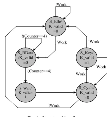
Since the design of this paper is based on the SM4 encryption and decryption circuit of the cyclic structure, and there is a reusable part in the circuit, an efficient state machine is required to control the entire encryption and decryption process. The flow of state machine for proposed design is shown in Fig. 4.
If the circuit is not working, the state machine is in the S_IDLE state, and the K_valid signal is 0. When the circuit starts the encryption operation, the state transition process is as follows: After the Work signal is 1, the state transitions to the S_RData state, at that time the circuit receives 32-bit plaintext serial data for four times and store it in the registers Xi, Xi+1, Xi+2, Xi+3. At the same time, 32-bit initial key data is
serially received for four times and performs XOR operation with FK and store it in registers Ki, Ki+1, Ki+2, Ki+3. After the
reception is completed, the state is switched to the S_Wait state, and the first round of key schedule operation is
performed. At this time, K_valid is 1. Then the next step is to perform key schedule and round transformation in turn under the control of the state machine. When the Work signal becomes 0, that end the encryption task, then the state machine re-enters the S_IDLE state. In proposed design, the decryption operation is almost the same as the encryption operation. However, in order to implement the decryption function, an encryption operation must be performed to obtain a decryption key and store it.
The Ck_Gen module performs the generation of Cki during
the cycle in which the round transformation is performed to reduce the critical path when performing key schedule. Each clock cycle determines whether key schedule or round conversion is determined based on whether K_valid is valid or not. When K_valid is 1, the input of TBox is Xi+1, Xi+2,
Xi+3, rki, and the round transformation operation is
performed; when K_valid is 0, the input of TBox is Ki+1, Ki+2,
Ki+3, Cki and the key schedule operation is performed. Then,
the key schedule and the round transformation are performed in the reused TBox, the input result is divided into two paths for linear operation.
IV. COMPARISONS AND RESULTS
In order to evaluate the resource consumption for proposed circuit architecture and verify the circuit function and performance, the above design is implemented using Verilog HDL. The functional simulation is carried out using Modelsim to verify the correct function. Using 100 random testcases, the circuit can correctly complete the SM4 encryption and decryption function everytime. Based on Xilinx Zynq-7000 platform, the proposed circuit is synthesized with Vivado 2017.4 and then implemented with constraints. The resource consumption and performance evaluation of the FPGA is shown in Table I and Table II, respectively.
S_RData /K_valid
=0
S_Wait/ K_valid=
1
S_Idle/ K_valid =0
S_Cycle/ K_valid
=0 S_Key/ K_valid =1 Work
!Work
!(Counter==4)
(Counter==4)
Work
Work !Work
[image:4.595.331.513.52.252.2]!Work
Fig. 4. State transition diagram
TABLE Ⅰ
THE RESOURCE OVERHEAD ON THE FPGA(XC7Z020CLG484)
Resource Type Overhead
LUT 539/53200(1.01%)
[image:4.595.308.545.727.771.2]Besides, based on SMIC 0.18 μm CMOS process, the design was synthesized using Synopsys Design Compiler with an area consumption of 57,290 μm2. Taking the NAND gate (9.9792 μm2) as the equivalent gate, the number of equivalent gates are 5740. The comparison between the proposed design and other architectures is given in Table III. It can be seen that the small-area SM4 encryption and decryption circuit is achieved which is superior in both circuit area and throughput/Gate, which further demonstrates that the design has good practicability.
V. CONCLUSIONS
In this paper, for the scenarios with strict requirements, an SM4 encryption and decryption algorithm circuit with low resource overhead and moderate data throughput is designed. This design allows 149 LUTs and 434 registers to achieve a data throughput rate of 147.82 Mbps on the Xilinx Zynq-7000 series FPGA. In SMIC 0.18μm CMOS process, our design can achieve 272.7Mbps throughput with an area of 0.057mm2. Compared with the implementation in [1], the proposed design reduces the area by 39.7%, and increased the throughput by 172%. It can be applied to sensor network nodes where the area, and power consumption are more stringent, as well as smart cards.
REFERENCES
[1] Chen-Guang W, Shu-Shan Q, Yong H. "Design of Low Complexity SM4 Block Cipher IP Core". Science Technology and Engineering, Vol.13, No.2, pp. 347-350, 2013.
[2] H. Fu, G. Bai and X. Wu, "Low-cost hardware implementation of SM4 based on composite field," 2016 IEEE Information Technology, Networking, Electronic and Automation Control Conference, Chongqing, 2016, pp. 260-264.
[3] Hao, Liang, et al. "Design and Implementation of SM4 Block Cipher Based on Composite Field." Microelectronics & Computer, Vol.32, No.5, pp. 16-20, 2015.
[4] Zhang X, Wu N, Zhou F, et al, "An optimized delay-aware common subexpression elimination algorithm for hardware implementation of binary-field linear transform." IEICE Electronics Express, vol. 11, No.22, pp. 1-8, 2014.
[5] Yaoping Liu, Ning Wu, Xiaoqiang Zhang, Fang Zhou. "A New Compact Hardware Architecture of S-Box for Block Ciphers AES and SM4", IEICE Electronics Express, Vol.14, No.11, pp. 1-6, 2017.
[6] Y. Shi, D. Zheng and C. Yang, "The Efficient Implementation of the Android Kernel with China Standard Cryptographic Algorithm," 2017 IEEE Second International Conference on Data Science in Cyberspace (DSC), Shenzhen, 2017, pp. 421-425.
[7] Y. Chen, Z. Zhang, L. Wu, X. Zhang and Y. Yang, "Analysis on Key-leakage Hardware Trojan of SM4 Algorithm," 2018 12th IEEE International Conference on Anti-counterfeiting, Security, and Identification (ASID), Xiamen, China, 2018, pp. 164-168.
[8] "National Institute of Standard and Technology. Advanced Encryption Standard. NIST FIPS PUB 197", 2001.
[9] Canright, David. (2005). A very compact S-box for AES. Lecture Notes in Computer Science. 3659. 441-455. 10.1007/11545262_32. [10] Satoh, Akashi & Morioka, Sumio & Takano, Kohji & Munetoh, Seiji.
(2001). A Compact Rijndael Hardware Architecture with S-Box Optimization. 239-254. 10.1007/3-540-45682-1_15.
[11] Y. XU, X.BAI, L. GUO, “A new algorithm of S-box for hardware implementation of SMS4,” Jo rnal of niversity of science and technology of china, Vol.39 No.11, pp. 1164-1170, 2009.
TABLE III PERFORMANCE COMPARISON
Proposed [1] [3]
Technology/μm 0.18 0.18 0.13
clock frequency/MHz 144.9 100 50
Area/μm2 57290 112976 46055
Equivalent-gate/gate 5740 8488 7612
Throughput/(Mb/s) 272.7 100 193.9 Throughput/gate/
(Mb·s-1·kgate-1) 47.51 11.78 25.47 TABLE Ⅱ
THE PERFORMANCE EVALUATION ON THE FPGA(XC7Z020CLG484)
Parameter Values
Highest clock frequency 78.5MHz
Critical path delay 12.734ns
Throughput 147.82Mb/s