Gate-Defined Quantum Confinement in InSe-based van
der Waals Heterostructures
Matthew Hamer*,1, 2, Endre Tóvári2, Mengjian Zhu1, Michael D. Thompson3, Alexander Mayorov4, Jonathon Prance3, Yongjin Lee5, Richard P. Haley3, Zakhar R. Kudrynskyi6, Amalia Patanè6, Daniel Terry1, 2, Zakhar D. Kovalyuk7, Klaus Ensslin5, Andrey V. Kretinin2,8, Andre Geim1,
Roman Gorbachev*,1, 2,
1School of Physics, University of Manchester, Oxford Road, Manchester, M13 9PL, UK
2National Graphene Institute, University of Manchester, Oxford Road, Manchester, M13 9PL, UK 3Department of Physics, University of Lancaster, Bailrigg, Lancaster, LA1 4YW, UK
4Centre for Advanced 2D Materials, National University of Singapore, 6 Science Drive 2, Singapore 5Solid State Physics Laboratory, ETH Zurich, Otto-Stern-Weg 1, 8093 Zürich, Switzerland
6School of Physics and Astronomy, University of Nottingham, NG7 2RD, UK
7National Academy of Sciences of Ukraine, Institute for Problems of Materials Science, UA-58001,
Chernovtsy, Ukraine
Indium selenide, a post-transition metal chalcogenide, is a novel two-dimensional (2D)
semiconductor with interesting electronic properties. Its tunable band gap and high electron
mobility have already attracted considerable research interest. Here we demonstrate strong
quantum confinement and manipulation of single electrons in devices made from few-layer crystals
of InSe using electrostatic gating. We report on gate-controlled quantum dots in the Coulomb
blockade regime as well as one-dimensional quantization in point contacts, revealing multiple
The electronic structure of two-dimensional (2D) metal chalcogenides (MCs) depends
strongly upon the number of atomic layers. In many MCs the bandgap can vary by as much as 1
eV and its type can change from direct to indirectF101,2. This opens many possibilities for band
gap engineering in the construction of complex electronic systems using the van der Waals
heterostructure platform3,4. In the last six years a large number of devices have been made from
few-layer MCs including photodetectors5, light emitting diodes6, field effect transistors7,8 and
indirect exciton devices9, to name but a few. There has also been a great deal of interest in charge
confinement within two-dimensional materials including one-dimensional (1D) channels in
quantum point contact (QPCs)10 and zero-dimensional quantum dots (QDs)11. Realizing such
systems could lead to novel quantum systems including spin-valley qubits12,13 and Luttinger
liquids14. The first laterally confined devices realized using 2D crystals were quantum dots
fabricated by etching graphene15,16. Those dots, however, suffered from limited performance and
poor reproducibility due to edge states and charge inhomogeneities introduced by plasma
etching17. The latter problem can be bypassed in semiconducting 2D crystals where the presence
of a band gap enables QDs to be electrostatically defined using gate electrodes. Successful
examples of gated defined quantum dots have been reported in 2D transition metal
dichalcogenides (TMDCs), i.e. WSe2 ,WS2 and most recently MoS2 18–20.
By contrast, 1D quantization has proven elusive: until very recently, graphene has been
the only 2D material to display signs of quantized conductance21–23. The difficulties in creating
QPCs that exhibit quality quantization are due to the following. First, series contact resistances
must be minimized to prevent 1D conductance steps from being obscured. Second, charge
transport needs to be ballistic with the mean free path exceeding the size of QPC constrictions.
Finally, the Fermi wavelength λF must be comparable to the constriction size, which typically
requires low charge densities. Therefore, the constriction size must be very small or the charge
carrier mobility very high: an imposing challenge from a fabrication perspective. In practical terms, these requirements rule out many 2D materials. Among the various TMDCs only a handful
up to ~5,000 cm2/Vs26 at T=4 K. Recently, however, improvements in device fabrication have led
to field-effect transistors made from MoS2 and InSe, which had over 20,000 cm2/Vs27,28, high
enough to observe the quantum Hall effect. Such mobilities make these materials promising
candidates for the observation of 1D quantization. Indeed, QPC conductance plateaus have been
reported in high-quality MoS2 channels20,29,30. .As for 2D InSe, this metal chalcogenide has a
semiconducting bandgap ranging from 1.25 eV in the bulk to 2.9 eV in single-layer samples28,31.
In addition, the bandgap remains quasi-direct down to few-layer thickness32, making InSe-based
devices promising for coupling with optics33,34. Less fortunately, 2D InSe degrades under ambient
conditions and, therefore, its exposure to air must be avoided, which requires fabrication in an
inert environment28.
In this report, we describe the first low-dimensional InSe devices defined by local
electrostatic gating. To avoid the degradation of the layers under ambient conditions, few-layer
InSe crystals were encapsulated in hexagonal boron nitride (hBN) using the dry peel transfer
technique inside an argon-filled glovebox chamber35. The top hBN encapsulation layer also serves
as a dielectric for the top gates deposited later. Ohmic contacts to 2D InSe were formed by
depositing the InSe crystals on top of two graphene flakes27,36, which subsequently were
contacted by Cr/Au electrodes as shown in Fig. 1a. To minimize the contact resistance, additional
top gates were deposited above each InSe/graphene interface to increase the carrier density and
suppress the Schottky barrier. The QDs and QPCs were electrostatically defined with a series of
top gates depicted in Fig. 1b. The overall carrier density n was controlled by the global back gate formed by the heavily doped silicon substrate. 2D InSe exhibits highest for a thickness of 5-6 layers28 and, accordingly, we focus below on results obtained from devices with these
thicknesses. The onset of Shubnikov-de Haas oscillations observed in devices (see Supplementary
Information) yields in the order of 10,000 cm2/Vs at T=1.5 K for electron densities of 𝑛 5x10¹²
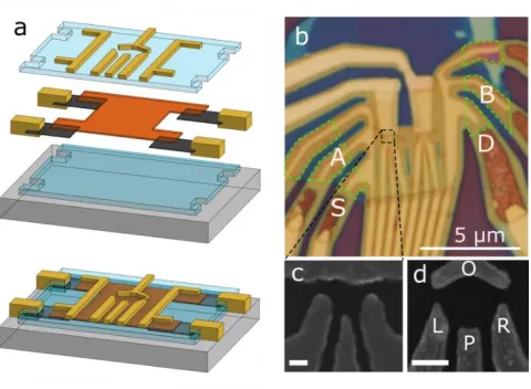
Figure 1. hBN/InSe/hBN heterostructure with graphene contacts and multiple top gates. (a) Schematic showing individual layers: 2D InSe (red), graphene (dark grey), hBN (blue), Cr/Au contacts and top gates (yellow), Si/SiO2 substrate (light grey). (b) Optical micrograph showing one of our van der Waals
heterostructures containing 6-layer InSe (dark yellow central region) which is sandwiched between thick (20-40nm) hBN crystals. The overlapping graphene contacts are outlined by the dashed green lines. Top gates serve to electrostatically define the quantum dot region and, also, tune the carrier density at the graphene/InSe interface. (c,d) Close-up SEM images of QD gates. Labels O, L, P, R stand for overall, left, plunger and right gates, respectively. Scale bars, 100 nm.
To define the QPCs, a negative voltage was applied to the top gates marked overall (O)
and left (L) in Fig. 1d, meanwhile the other top gates (P and R) were held at zero potential. The
total charge density was controlled by the back gate. Fig. 2a plots an example of the differential
conductance G of such QPCs as a function of the split gate voltage VLO simultaneously applied to
both O and L top gates (see Fig. 1d) at several fixed back-gate voltages VBG. All of the curves exhibit step-like features close to integer multiples of the conductance quantum 2e2/h 77.46
µS, which suggests 1D spin-degenerate channels (h is the Planck constant and e the elementary charge). The shift of the conductance curves towards negative VLO at higher VBG is due to the
increasing electron density induced by the back gate. The quality of quantization is similar to, if
not better than, that observed in graphene-based QPCs in zero magnetic field21–23. It is of note,
that the step-like features are more pronounced at higher n (dark blue curve in Fig. 2a), which makes it unlikely that mesoscopic conductance fluctuations contribute to these steps. The
decrease in quality of the QPC features at lower 𝑛 can be attributed to shortening of the mean
The latter value is comparable to the size of our constrictions (see below). For the above
estimates, we have used a reference device made in the Hall bar geometry and exhibiting similar
(see SI), and applied the Drude formula 𝑙 = ℎσ √2𝜋𝑛𝑒⁄ 2, where σ is the conductivity. The conductance steps were reproducible for different constrictions and devices however, the
quantization quality could notably differ (orange curve in Fig. 2a), presumably because of
[image:5.612.77.540.257.421.2]disorder within the QPC regions.
Figure 2. Conductance quantization in InSe point contacts. (a) Differential conductance of a QPC made
from 6-layer InSeat 2K (lines with symbols). The series (parasitic) resistance 𝑅p≈ 1kΩ was subtracted for each VBG (See Supplementary Information: Methods). Dashed red line: calculated positions and widths of plateaus in the ideal case. Solid black curve: plateau shapes expected in our devices. Orange curve: another QPC device. (b) Electrostatic simulation of a symmetric constriction, showing the offset φ of the
conductance band. White lines: =0. (c) One dimensional potential extracted from (b) across the dashed line. (d) Uncorrected (Rp = 0) conductance of QPC1 at VBG=75 V as a function of the applied DC voltage VDC
along the constriction. VLO changes from -4.5 to -3.8 V in steps of 0.02 V (no offset). For all the
measurements, the AC excitation was 100 μV, and 6 V was applied to the overlap gates above the
InSe/graphene contacts.
-4.0 -3.5 -3.0 -2.5 -2.0 0 2 4 6 8 10
QPC 1, Vbg (V) 70 68 66 64 62 60 QPC 2, Vbg (V)
70 Gc o rr (e 2/h)
VLO (V)
-6 -4 -2 0 2 4 61 2 3 4 5 6 G xx (e 2 /h)
VBG= 70 V
d
VLO= -3.8 V
VLO= -4.5 V
VDC (mV)
VBG=75 V
a
VO= -4.15 V
-100 0 100 -100
-50 0 50
VL= -4.15 V
b
y
(n
m)
x (nm)
0.0 0.2 0.4 0.6 0.8
(eV)
-25 0 25
-40 -20 0
y (nm)
c
VLO:
To support our observations, we calculated numerically the 1D quantization conductance
expected in our experimental constrictions, with SEM and AFM imaging being used to extract the
size and shape of the constrictions. The self-consistent potential, 𝛷, was calculated using the 3D
Poisson equation with boundary conditions based on the electron density of states in the InSe
layer:
𝜌 = −𝑒𝑚
𝜋ℏ2𝑒𝛷 H(𝛷),
Where 𝑚 = 0.14𝑚𝑒 is the effective mass in 2D InSe28, 𝑚𝑒 is the free electron mass, H(𝛷) is a
step function that is zero when the potential is negative (fully depleted) and unity otherwise
(when charge carriers are present) and 𝛷 is essentially the Fermi energy with respect to the
conduction band edge. The potential calculated for the QPC narrowing (dashed line in Fig. 2b)
was then used to solve the 1D Schrödinger equation and find the number of transverse modes
propagating through the QPC. Except for the QPC pinch-off voltage, this model has no adjustable
parameters. The resulting conductance plateaus are shown by the red dashed curve in Fig. 2a.
For a more realistic description of the QPC, we used the parabolic saddle-point potential
model37. The potential cuts were taken from our simulations of 𝛷 for V
BG = 70 V and then
approximated with parabolas within the vicinity of the constriction center (Fig. 2b). This was
repeated for different values of VLO, which allowed us to find the dependence G(VLO). A result of
this modelling is shown in Fig. 2a by the black solid curve (for clarity, it is shifted by –0.5 V along
the x-axis), showing good agreement with the experimental dependence. Note that our
approximation of the parabolic saddle-point potential gets progressively worse with increasing
VLO range.
For completeness, Fig. 2d shows the bias voltage spectroscopy for one of our QPCs at VBG
=75 V and various split-gate voltages VLO. These measurements allow us to estimate the energy
spacing between the 1D subbands i.e. 5-10 meV, in good agreement with our solution to the 1D Schrödinger equation, which gives a separation of =10 meV between the first and second
1D subband.
In further experiments, quantum dots were formed by the depletion of the 2D electron
gas underneath all four top gates in Figs 1c,d. The coupling of such QDs to the source and drain
fixed throughout the measurements. The plunger gate was used to tune the chemical potential
inside the QDs. Initial tuning and symmetrization were carried out by recording the two-terminal
differential conductance through the QD as a function of both VL and VR, as shown in Fig. 3a. The
conductance plot exhibits a series of bright lines that correspond to a finite conductance in the
Coulomb blockade (CB) regime. We use this plot to select the gate voltages that lead to
lithographically defined QDs and, thus, to avoid unintentional QDs due to disorder. The latter can
appear inside the two constrictions. We expect that CB oscillations with a slope close to -1 in Fig.
3a originate from the intentional, lithographically defined QDs because the CB oscillations are
equally affected by both gates. This indicates that the dot is localized somewhere between the
two gates (an example is indicated by the white line in Fig. 3a). In contrast, horizontal or vertical
lines in Fig. 3a correspond to unintentional QDs which are controlled by only one of the gates
and, therefore, are localized in proximity. The latter QDs were discarded from our analysis. The
[image:7.612.87.538.382.537.2]region of gate voltages used in our analysis is marked by the circle in Fig. 3a.
Figure 3. Gate-defined quantum dots in 2D InSe. (a) Map of the two-terminal differential conductance as a function of voltages VR and VL which control the left and right barriers. Other gates were fixed at VBG = 50 V, VO= -4.51 V, VP= -2 V; 10 μV AC excitation. The diagonal lines are due to gate defined QDs and therefore react to both side gates, as designed. Accidental QDs are caused by disorder and are more sensitive to one gate. (b) Conductance in the region highlighted by the circle in (a). Coulomb diamonds extend to the edges of the scanned range (dashed white lines). Temperature, 50 mK. (c) Charge carrier
-3.2 -3.1 -3.0 -2.9 -2.8 -2.7 -3.7 -3.6 -3.5 -3.4 -3.3 VSD (m V)
G (S)
VR (V)
VL
(V)
0.0 0.5 1.0 1.5 2.0
-200 -100 0 100 200 -200 -100 0 100 200 -3.6V -3.6V
VBG=23 V
-4.5V
x (nm)
y
(nm)
-2.7V
0 4 8 12
-2.35 -2.30 -0.8 -0.4 0.0 0.4 0.8
n (1011cm-2)
G (S)
VP (V)
Fig. 3b shows Coulomb diamonds observed in this region. The InSe QD exhibits an average
plunger gate periodicity ΔVP of 19 mV. Using these measurements, we estimate an average charging energy Ec of 0.8 meV, which yields the dot’s self-capacitance of CΣ = e2/Ec of 177 aF
and plunger capacitance CP = e/VP ≈ 8 aF. However, the irregular shape of the diamonds suggests
that the charging energy is comparable to the QD’s confinement energy ΔE, which makes the above values only an approximation38. This is the case because the estimates are based on the
assumption ΔE≪Ec. No additional resonance lines indicating excited states were observed within the conducting regions. This can be explained by a large tunneling amplitude t over the left and right barriers at nonzero VSD, which leads to a decrease in the lifetime of localized states and blurs fine features. The finite t is also the reason why the conductance is finite within the diamonds (t≪Ec implies no conductance). We have also calculated a charge density map for realistic values of our gate voltages (Fig. 3c). The figure shows an island in the electron gas which has a size of
100 nm and contains 60 electrons, in qualitative agreement with the above estimate for R. Changing the plunger gate values in our model, we have found similar gate coupling of CP ≈ 6 aF
The found value of CΣ can be used to estimate the QD size by evoking the self-capacitance
of an isolated disk with radius R in a dielectric medium11, Cdisc=8Rε
0εr, where ε0 andεr10 are the
permittivity’s of a vacuum and InSe, respectively39. The total capacitance defining the charging
energy is the sum of all the gate capacitances and the QD self-capacitance. For the purpose of
our estimation, we assume that the barrier and plunger gate capacitances are approximately the
same (10 aF) and the overall gate capacitance is three times larger. Consequently, the self-capacitance of the InSe disk, Cdisk, should be around 120 aF, yielding R 170 nm.
In conclusion, we have demonstrated both one-dimensional and zero-dimensional
confinement in few-layer InSe. The relatively small in-plane electron mass and high electron
mobility in 2D InSe enables the one-dimensional quantization of electrons by electrostatic gating.
In addition, using local top gates strategically placed over the InSe/graphene overlap, we have
been able to significantly reduce contact resistance to InSe. Following from these promising
results, it seems that two-dimensional materials are an excellent platform to study 1D and 0D
physics. As such we envisage that InSe will play a strong role in the future of two-dimensional
Corresponding Author
*Email: [email protected], [email protected]
Funding Sources
This project has received funding from the European Union’s Horizon 2020 research and
innovation programme under grant agreement No 696656, and under the Marie
Skłodowska-Curie grant agreement No 751883 (PTMCnano). In addition, funding has been received from the
Engineering and Physical Sciences Research Council [grant number EP/M012700/1] (EPSRC).
Acknowledgements
We acknowledge the support of “The Wolfson Foundation”, the “J P Moulton Charitable
Foundation”, and the “Garfield Weston Foundation” in establishing the IsoLab facility. We also
References
(1) Splendiani, A.; Sun, L.; Zhang, Y.; Li, T.; Kim, J.; Chim, C.; Galli, G.; Wang, F. Emerging Photoluminescence in Monolayer MoS2. Nano Lett.2010, 10 (4), 1271–1275.
(2) Tongay, S.; Zhou, J.; Ataca, C.; Lo, K.; Matthews, T. S.; Li, J.; Grossman, C.; Wu, J. Thermally Driven Crossover from Indirect toward Direct Bandgap in 2D Semiconductors: MoSe2
versus MoS2. Nano Lett.2012, 12 (11), 5576–5580.
(3) Geim, A. K.; Grigorieva, I. V. Van Der Waals Heterostructures. Nature 2014, 499 (7459), 419–425.
(4) Novoselov, K. S.; Mishchenko, A.; Neto, C.; Carvalho, A.; Castro Neto, A. H. 2D Materials and van Der Waals Heterostructures. Science (80-. ).2016, 353 (6298).
(5) Choi, W.; Cho, M. Y.; Konar, A.; Lee, J. H.; Cha, G.; Hong, S. C.; Kim, S.; Kim, J.; Jena, D.; Joo, J.; et al. High-Detectivity Multilayer MoS 2 Phototransistors with Spectral Response from Ultraviolet to Infrared. Adv. Mater.2012, 24 (43), 5832–5836.
(6) Withers, F.; Del Pozo-Zamudio, O.; Mishchenko, A.; Rooney, A. P.; Gholinia, A.; Watanabe, K.; Taniguchi, T.; Haigh, S. J.; Geim, A. K.; Tartakovskii, A. I.; et al. Light-Emitting Diodes by Band-Structure Engineering in van Der Waals Heterostructures. Nat. Mater.2015, 14 (3), 301–306.
(7) Ovchinnikov, D.; Allain, A.; Huang, Y.-S.; Dumcenco, D.; Kis, A. Electrical Transport Properties of Single-Layer WS2. ACS Nano2014, 8 (8), 8174–8181.
(8) Roy, T.; Tosun, M.; Kang, J. S.; Sachid, A. B.; Desai, S. B.; Hettick, M.; Hu, C. C.; Javey, A. Field-Effect Transistors Built from All Two-Dimensional Material Components. ACS Nano 2014, 8 (6), 6259–6264.
(9) Rivera, P.; Schaibley, J. R.; Jones, A. M.; Ross, J. S.; Wu, S.; Aivazian, G.; Klement, P.; Seyler, K.; Clark, G.; Ghimire, N. J.; et al. Observation of Long-Lived Interlayer Excitons in Monolayer MoSe2–WSe2 Heterostructures. Nat. Commun.2015, 6, 6242.
(10) Ando, T. Quantum Point Contacts in Magnetic Fields. Phys. Rev. B1991, 44 (15).
(11) Kouwenhoven, L. E. O. P.; Marcus, C. M.; Mceuen, P. L.; Tarucha, S.; Robert, M. Electron Transport In Quantum Dots; 1997.
(13) Kormányos, A.; Zólyomi, V.; Drummond, N. D.; Burkard, G. Spin-Orbit Coupling, Quantum Dots, and Qubits in Monolayer Transition Metal Dichalcogenides. Phys. Rev. X2014, 4 (1), 1–16.
(14) Braunecker, B.; Simon, P.; Loss, D. Nuclear Magnetism and Electron Order in Interacting One-Dimensional Conductors. Phys. Rev. B2009, 80 (16), 165119.
(15) Ponomarenko, L. A.; Schedin, F.; Katsnelson, M. I.; Yang, R.; Hill, E. W.; Novoselov, K. S.; Geim, a K. Chaotic Dirac Billiard in Graphene Quantum Dots. Science (80-. ).2008, 320 (5874), 356–358.
(16) Güttinger, J.; Frey, T.; Stampfer, C.; Ihn, T.; Ensslin, K. Spin States in Graphene Quantum Dots. Phys. Rev. Lett.2010, 105 (11), 116801.
(17) Bischoff, D.; Varlet, A.; Simonet, P.; Eich, M.; Overweg, H. C.; Ihn, T.; Ensslin, K. Localized Charge Carriers in Graphene Nanodevices. Appl. Phys. Rev.2015, 2 (3), 31301.
(18) Song, X.-X.; Liu, D.; Mosallanejad, V.; You, J.; Han, T.-Y.; Chen, D.-T.; Li, H.-O.; Cao, G.; Xiao, M.; Guo, G.-C.; et al. A Gate Defined Quantum Dot on the Two-Dimensional Transition Metal Dichalcogenide Semiconductor WSe2. Nanoscale2015, 7 (40), 16867–16873.
(19) Song, X.-X.; Zhang, Z.-Z.; You, J.; Liu, D.; Li, H.-O.; Cao, G.; Xiao, M.; Guo, G.-P. Temperature Dependence of Coulomb Oscillations in a Few-Layer Two-Dimensional WS2 Quantum Dot. Sci. Rep.2015, 5 (1), 16113.
(20) Wang, K.; De Greve, K.; Jauregui, L. A.; Sushko, A.; High, A.; Zhou, Y.; Scuri, G.; Taniguchi, T.; Watanabe, K.; Lukin, M. D.; et al. Electrical Control of Charged Carriers and Excitons in Atomically Thin Materials. Nat. Nanotechnol.2018, 1.
(21) Tombros, N.; Veligura, A.; Junesch, J.; Guimarães, M. H. D.; Vera-Marun, I. J.; Jonkman, H. T.; van Wees, B. J. Quantized Conductance of a Suspended Graphene Nanoconstriction. Nat. Phys.2011, 7 (9), 697–700.
(22) Allen, M. T.; Martin, J.; Yacoby, A. Gate-Defined Quantum Confinement in Suspended Bilayer Graphene. Nat. Commun.2012, 3, 934.
(25) Iqbal, M. W.; Iqbal, M. Z.; Khan, M. F.; Shehzad, M. A.; Seo, Y.; Park, J. H.; Hwang, C.; Eom, J. High-Mobility and Air-Stable Single-Layer WS2 Field-Effect Transistors Sandwiched
between Chemical Vapor Deposition-Grown Hexagonal BN Films. Sci. Rep.2015, 5 (April), 9.
(26) Cao, Y.; Mishchenko, A.; Yu, G. L.; Khestanova, E.; Rooney, A. P.; Prestat, E.; Kretinin, A. V.; Blake, P.; Shalom, M. B.; Woods, C.; et al. Quality Heterostructures from Two-Dimensional Crystals Unstable in Air by Their Assembly in Inert Atmosphere. Nano Lett.2015, 15 (8), 4914–4921.
(27) Cui, X.; Lee, G.; Kim, Y. D.; Arefe, G.; Huang, P. Y.; Lee, C.; Chenet, D. A.; Zhang, X.; Wang, L.; Ye, F.; et al. Multi-Terminal Transport Measurements of MoS2 Using a van Der Waals Heterostructure Device Platform. Nat. Nanotechnol.2015, 10 (6), 534–540.
(28) Bandurin, D. A.; Tyurnina, A. V.; Yu, G. L.; Mishchenko, A.; Zólyomi, V.; Morozov, S. V.; Kumar, R. K.; Gorbachev, R. V.; Kudrynskyi, Z. R.; Pezzini, S.; et al. High Electron Mobility, Quantum Hall Effect and Anomalous Optical Response in Atomically Thin InSe. Nat. Nanotechnol.2016, 50 (17), 1–18.
(29) Epping, A.; Banszerus, L.; Güttinger, J.; Krückeberg, L.; Watanabe, K.; Taniguchi, T.; Hassler, F.; Beschoten, B.; Stampfer, C. Quantum Transport through MoS2 Constrictions Defined by
Photodoping. 2016.
(30) Pisoni, R.; Lee, Y.; Overweg, H.; Eich, M.; Simonet, P.; Watanabe, K.; Taniguchi, T.; Gorbachev, R.; Ihn, T.; Ensslin, K. Gate-Defined One-Dimensional Channel and Broken Symmetry States in MoS2 van Der Waals Heterostructures. Nano Lett.2017, 17 (8), 5008–
5011.
(31) Zólyomi, V.; Drummond, N. D.; Fal’ko, V. I. Electrons and Phonons in Single Layers of Hexagonal Indium Chalcogenides from Ab Initio Calculations. Phys. Rev. B2014, 89 (20), 205416.
(32) Mudd, G. W.; Molas, M. R.; Chen, X.; Zólyomi, V.; Nogajewski, K.; Kudrynskyi, Z. R.; Kovalyuk, Z. D.; Yusa, G.; Makarovsky, O.; Eaves, L.; et al. The Direct-to-Indirect Band Gap Crossover in Two-Dimensional van Der Waals Indium Selenide Crystals. Sci. Rep. 2016, 6 (39619), 1–10.
(33) Kosaka, H.; Shigyou, H.; Mitsumori, Y.; Rikitake, Y.; Imamura, H.; Kutsuwa, T.; Arai, K.; Edamatsu, K. Coherent Transfer of Light Polarization to Electron Spins in a Semiconductor. Phys. Rev. Lett.2008, 100 (9), 96602.
Oiwa, A.; Tarucha, S. Single Electron-Photon Pair Creation from a Single Polarization-Entangled Photon Pair. Sci. Rep.2017, 7 (1), 16968.
(35) Ponomarenko, L. A.; Geim, A. K.; Zhukov, A. A.; Jalil, R.; Morozov, S. V.; Novoselov, K. S.; Grigorieva, I. V.; Hill, E. H.; Cheianov, V. V.; Fal’ko, V. I.; et al. Tunable Metal–insulator Transition in Double-Layer Graphene Heterostructures. Nat. Phys.2011, 7 (12), 958–961.
(36) Mudd, G. W.; Svatek, S. A.; Hague, L.; Makarovsky, O.; Kudrynskyi, Z. R.; Mellor, C. J.; Beton, P. H.; Eaves, L.; Novoselov, K. S.; Kovalyuk, Z. D.; et al. High Broad-Band Photoresponsivity of Mechanically Formed InSe – Graphene van Der Waals Heterostructures. Adv. Mater. 2015, 27 (25), 3760–3766.
(37) Büttiker, M. Quantized Transmission of a Saddle-Point Constriction. Phys. Rev. B1990, 41 (11), 7906–7909.
(38) Sapmaz, S.; Jarillo-Herrero, P.; Kouwenhoven, L. P.; Zant, H. S. J. van der. Quantum Dots in Carbon Nanotubes. Semicond. Sci. Technol.2006, 21 (11), S52–S63.