Matthew D. Watson,1,∗ Adam M. Beales,1 and Philip D. C. King1,† 1
SUPA, School of Physics and Astronomy, University of St. Andrews, St. Andrews KY16 9SS, United Kingdom (Dated: May 8, 2019)
Resistivity measurements of TiSe2typically show only a weak change in gradient at the charge density wave
transition atTCDW ≈200 K, but more prominently feature a broad peak at a lowerTpeak ∼165 K, which has remained poorly understood despite decades of research on the material. Here we present quantitative simulations of the resistivity using a simplified parametrization of the normal state band structure, based on recent photoemission data. Our simulations reproduce the overall profile of the resistivity of TiSe2, including
its prominent peak, without implementing the CDW at all. We find that the peak in resistivity corresponds to a crossover between a low temperature regime with electron-like carriers only, to a regime around room temperature where thermally activated and highly mobile hole-like carriers dominate the conductivity. Even when implementing substantial modifications to model the CDW below the transition temperature, we find that these thermal population effects still dominate the transport properties of TiSe2.
Phase transitions such as charge density waves (CDWs) are often first characterized by the observation of anomalies in re-sistivity measurements. Such phase transitions can influence the resistivity via Fermi surface reconstructions, changes in scattering rates, and/or a loss of free carriers due to the for-mation of an energy gap. However in TiSe2, which exhibits a much-studied CDW-like phase transition atTCDW ≈200 K [1, 2], transport measurements show a highly unusual and non-monotonic temperature-dependence. Samples which are close to stoichiometry typically shown-type metallic-like be-havior at low temperatures, followed by a prominent broad peak atTpeak ∼165 K, distinct fromTCDW, beyond which the resistivity decreases with increasing temperature in a semiconductor-like fashion, with a positive Hall coefficient at room temperature [1]. Surprisingly little change occurs at TCDW, with at most a modest change in slope observed at
≈200 K [1,3], even though the CDW involves changes to the band structure on energy scales as large as 100 meV [4]. The resistivity is known to be highly sensitive to the sample stoi-chiometry, and the observation of the anomalous broad peak atTpeak ∼165 K in resistivity measurements has sometimes been taken as an indicator of sample quality [1,3,5,6]. On the other hand, some studies have interpreted the peak feature as a signature of the role of excitons in the CDW ordering [7–
11]. Given the resurgence of interest in TiSe2in recent years, it is worthwhile to revisit the long-standing problem of its un-usual transport properties [5,12–14], aided by the availability of recent characterizations of its 3D electronic structure by angle-resolved photoemission spectroscopy (ARPES) [15].
In this paper, we show that the overall temperature-dependence of the resistivity of TiSe2, including the anoma-lous peak, can be reasonably reproduced without accounting for the CDW at all. Our model is very simple, but it cap-tures the essential ingredients necessary to qualitatively un-derstand the transport properties of TiSe2. While TiSe2 has been variously discussed as either an indirect semiconduc-tor or semimetal [4], we start from a picture of a narrow-band gap semiconductor, with a small extrinsic electron dop-ing, based on the most recent experimental electronic struc-ture studies. The unusual resistivity profile is mainly due to
the temperature-dependent thermal populations of the 2D hole and 3D electron bands, which vary significantly since the band gap is only∼ 3 ×kBT at room temperature. The appar-ently anomalous transport behavior of TiSe2can thus be intu-itively understood as a consequence of the thermal activation of mobile hole-like carriers above a characteristic temperature of∼150 K, which sets the scale ofTpeak. Tpeakthus repre-sents a crossover from electron-dominated to hole-dominated transport properties, which also manifests as a sign change in the Hall coefficient at a similar temperature, as found in ex-periments. We show that changes in the band structure due to the CDW may modulate the resistivity belowTCDW and shiftTpeak a little, but the qualitative understanding of the anomalous peak remains unchanged. We finally discuss the appropriate criteria for extractingTCDW from resistivity ex-periments, with implications for the determining the bound-aries of phase diagrams based on TiSe2.
Model parameters and carrier densities
Energy (meV) 0
1 2 3
DOS (10
22 cm -3/eV)
T = 300 K
Energy (meV)
T = 10 K
0 0.5 1
k (Å-1) 400
300 200 100 0
Binding Energy
(meV)
T = 300 K nh ne nh = 0 ne = Nd
T (K) 0 20 40 60 80
-100 -50 0 50 100 150 200 -100 -50 0 50 100 150 200
µ
(meV)
0 100 200 300
[image:2.612.71.561.52.173.2](a) (b) (c) (d)
FIG. 1. Model band structure of TiSe2. (a) ARPES data at 300 K, adapted from [15], overlaid with parabolas corresponding to the assumed
dispersions of the hole and electron-like carriers respectively. (b) Available Density of States for the 2D hole band (cyan line) and 3D electron band (orange line), also showing the thermally occupied population of each carrier type (shaded areas) at 300 K, and (c) 10 K. The dashed line indicates the location of the chemical potential. (d) Chemical potential as a function of temperature. Note that in (b-d), the top of the valence band is defined to be at zero energy, whereas in (a) the data is referenced to the experimental chemical potential.
measurements in the normal phase [15]. Parabolas represent-ing the assumed dispersions are plotted on top of ARPES data at 300 K in Fig. 1(a). TiSe2 samples are never exactly sto-ichiometric, and to the best of our knowledge are always at least slightly n-doped, as indicated by the negative value of the Hall coefficient at low temperatures [1]. We therefore al-low for a finite, temperature-independent, number of donors into our model. We set the extrinsic carrier density such that 1/Nd|e|equals the low-temperature Hall coefficient reported in Ref. [1], givingNd= 7.6×1019cm−3.
While the model is clearly a simplification, we are careful to retain two key ingredients: the temperature-dependence of the chemical potential, and the corresponding thermal pop-ulations of hole and electron carriers [7]. At each tempera-ture, the chemical potential is determined by the requirement thatne(T)−nh(T) =Nd. This charge compensation condi-tion leads to a downward shift of the chemical potential with increasing temperature (Fig. 1(d)). At low temperatures, in Fig.1(c), there is essentially zero thermal population of the hole-like carriers, and ne = Nd. However, by room tem-perature, since the band gap is only ∼ 3×kBT, the tails of the Fermi-Dirac state occupation function extend into the hole-like DOS and thermally populate a significant number of hole-like carriers, as shown in Fig.1(b). This thermal popula-tion of hole-like carriers plays a leading role in the following simulations.
Simulation of resistivity
We simulateρ(T), the resistance as a function of tempera-ture, using the two-carrier Drude model:
1 ρ(T) =
ne(T)|e|2τ(T) m∗
e
+nh(T)|e|
2τ(T)
m∗h (1)
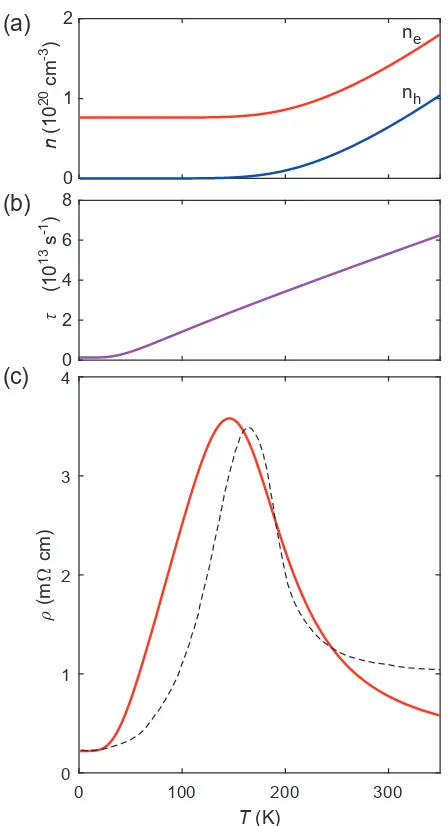
The temperature-dependence of the electron and hole pop-ulationsne,h(T)is shown in Fig.2(a). For the scattering time,
τ(T), we take inspiration from the resistivity of TiTe2, a sister material which is semimetallic, with a band overlap of several hundred millivolts. In Ref. [16] it was shown that the resis-tivity of TiTe2followed the Bloch-Gr¨uneisen (B-G) formula-tion which models the scattering of electrons from acoustic phonons. We therefore adopt this form of scattering rate for our model of TiSe2: the coefficient of the B-G scattering term is a free parameter which we set for good agreement on the absolute value of resistivity aroundρpeak, and the Debye tem-perature of the B-G term is set to 250 K [2,14]. We also add a constant scattering term from elastic impurity scatter-ing, which is set such thatρexpT→0 = me∗/Ne|e|2τ0. Notably, this scattering rate, plotted in Fig.2(b), is almost linear in tem-perature across an appreciable range, and featureless through-out the region of interest. We make the assumption that this scattering rate is identical for both electron and hole-like car-riers. Importantly, however, the two types of carrier will have quite different mobilities [13], sinceµe,h = |e|τ /m∗e,h, and the effective masses of the electrons are much higher than the holes.
The simulatedρ(T)is shown in Fig.2(c), plotted in com-parison to the experimental literature data from Di Salvo et al. [1] [17]. The simulation reproduces the low-and high-temperature regimes reasonably well, and importantly in-cludes a peak at 146 K, close toTpeak = 165 K in the ex-perimental data. Given the crudeness of the model, and the total neglect of CDW effects, the agreement is remarkable.
0 100 200 300 T (K)
0 1 2 3 4
(m
cm)
0 1 2
n
(10
20 cm -3 )
ne
nh
0 2 4 6 8
τ
(10
13 s -1 )
(a)
(b)
(c)
FIG. 2. (a) Temperature-dependence of electron- and hole-like car-rier densities (see Fig.1(b-c) for visualization at two selected tem-peratures). (b) The assumed scattering rates, following the Bloch-Gr¨uneisen formula for electron-phonon scattering with an additional elastic impurity scattering term. (c) Corresponding simulation of re-sistivity. Dashed line is the experimental resistivity, from Ref. [1].
increases above∼150 K (Fig.2(b)). These two effects com-bine to overcome the near-linearly increasing scattering rate in this regime, yielding a maximum in resistivity atTpeak. This is followed by a regime of negativedρ/dT up to room tem-perature and beyond, as the hole-like carrier density increases at a greater rate than the scattering.
While the overall agreement in Fig 2 is good, at high tem-peratures the modelled resistivity is somewhat less flat than the experimental case. The temperature-dependence of the resistivity in this regime reflects the balance between the temperature-dependent changes in the carrier densities due to thermal population effects with the temperature-dependent changes of the scattering rate. The deviations between the
model and experiment observed in this range thus likely re-flect simplifications made in our choice of the scattering rate, which is the least constrained quantity from experiments here. In Fig. 3we show model calculations of the resistiv-ity upon making different assumptions for the scattering rate. Fig.3(c,d) shows that the additional consideration of scatter-ing from optical phonons tends to increase and flatten the re-sistivity at high temperature, giving a better match to the ex-periments in this regime, while also improving the agreement in the low-temperature limit. An alternative assumption of a Fermi liquid-likeT2scattering rate in Fig.3(e,f), attributable to electron-electron scattering, also yields a much flatter curve around room temperature and above. In practice, a num-ber of scattering mechanisms will simultaneously contribute, which also may not necessarily be equal for hole and elec-tron carriers. Our original formalism, including only acoustic phonons and an impurity scattering term, will thus generally underestimate the resistivity in the high-temperature regime, as shown in Fig.2 and reproduced in Fig.3(a,b). However, for simplicity in the following simulations we return to this assumption. The crucial observation is that for any reason-able monotonically-increasing scattering rate, a pronounced peak in the resistivity is found, the origin of which lies in the temperature-dependence of the carrier densities and not the scattering rate.
Variation with net carrier density
The net carrier density Nd is an extrinsic and variable parameter of TiSe2 samples. In the standard iodine vapor transport growth method, higher growth temperatures corre-spond to a larger density ofn−doping defects [18], drasti-cally changing the resistivity [1,11]. Post-growth annealing [19], deliberate introduction of other transition metal dopants or intercalants [6,20,21], and ionic gating [22] have also been used to control the carrier density. To gain some understand-ing into the variation of the transport properties with this key experimental parameter, in Fig.4(a) we consider the effect of varyingNdin our simulations.
[image:3.612.65.289.48.461.2]0 100 200 300
T (K)
(m
-cm)
0 100 200 300
T (K)
(m
-cm)
0 100 200 300
T (K) 0
1 2 3
(m
-cm)
0 5 10
acoustic optical
total
τ
(10
13 s
-1) (a) (c) (e)
(b) (d) (f)
FIG. 3. a) The scattering rate due to acoustic phonons according to the Bloch-Gr¨uneisen formula, and b) calculated resistivity (both reproduced from Fig.2). c,d) Equivalent plots, in which scattering from both acoustic and optical phonons is considered. e,f) Equivalent plots in which the scattering rate is assumed to be proportional toT2. In all cases a constant impurity scattering term is also included.
sample quality [1,3,6]. Our simulations show that there is a monotonic inverse dependence ofρpeak/ρ300KonNd, show-ing that this is indeed a useful indicator of the closeness of the sample to charge compensation. For a substantial doping of Nd = 5×1020 cm−3, corresponding to 0.033 carriers per formula unit, the peak behavior disappears and the resistivity appears generally metallic below room temperature. This is in line with the measured metallic-like resistivity of samples with the highest doping levels [1,5,11,19,20]. Conversely, our model suggests that any sample which has an extrinsic electron doping of less than 0.01 electrons per formula unit will display a prominent peak.
The second trend in Fig.4(a) is that the lower the carrier density, the lower Tpeak. In the model, we find the fewer the number of doped electrons, the fewer thermally activated hole-like carriers are needed to influence the resistivity, and so the peak occurs at a lower temperature. Our simulations may exaggerate this effect somewhat since, as we show later, the CDW transition modulates the exact position ofTpeak, which may tend to dampen the variation found in Fig.4(a). Still, the trend is consistent with experimental evidence. For example, the sample grown by sublimation in Di Salvoet al. [1] with Tpeak≈149 K, and the sample grown in Se flux by Campbell
et al. (Tpeak = 150 K [14]), which are likely to be the most
stoichiometric samples (i.e. lowest extrinsic carrier densities), both display a higherρpeakand a lowerTpeakcompared with samples grown by iodine vapor transport, in whichTpeak is typically 165 K [1].
Robustness of the peak feature
In addition to the net carrier density, another important pa-rameter in our model is the band gap. We take our value of 74 meV from high-resolution ARPES measurements at 300 K [15], but there is considerable disagreement on the magnitude of the normal state band gap in the prior literature [4]. In Fig.4(b) we vary the band gap and find that a peak feature in the resistivity is generically expected, for any relatively nar-row band gap. Gap values of 50-100 meV giveTpeak compa-rable with the experimental data, correlating with the determi-nation of 74 meV from ARPES [15]. It is intuitive thatTpeak scales with the gap, since for a larger gap, higher temperatures are required to activate a significant hole carrier density.
Furthermore, we show in Fig. 4(b) that for a small band overlap (negative band gap), no peak appears in our simula-tions and the resistivity is a monotonically increasing function of temperature, in total disagreement with the experimental re-sistivity. The simulations thus support the simple intuition that the negativedρ/dT around room temperature is indicative of a narrow band gap in the normal state. While a semimetal-lic scenario for the normal state was proposed by Velebit
et al.[24], this could only be reconciled with the resistivity
[image:4.612.70.549.52.283.2](a)
0 50 100 150 200 250 300
T (K)
0 2 4 6 8
(m
-cm)
2.5×10¹⁹
7.5×10¹⁹
1.5×10²⁰
5×10²⁰
0 50 100 150 200 250 300
T (K)
0 1 2 3 4 5 6
-2525 50 75 100 125
0 50 100 150 200 250 300
T (K)
0 1 2 3 4
3.8 2.5 1.25
x10 Nd (cm-3) = E
g (meV) = m*e (me) =
(c) (b)
FIG. 4. (a) Simulated resistivity curves for various values of the extrinsic dopingNd. All other parameters are held fixed, including the elastic impurity scattering term, which in reality would be likely to scale withNd. (b) Variation of the resistivity with the band gap. Note that for the case of the band overlap, the resistivity is multiplied by a factor of 10 for greater visibility. (c) Simulations with various assumed values of the electron mass.
of the successful simulations in this paper, as well as the ev-idence from photoemission [15], we would argue that a nar-row band gap and a conventional temperature-dependence of the scattering rates (apart from, perhaps, at temperatures very close toTc) is the scenario that best accounts for the normal state electronic structure and transport properties of TiSe2. We note that it is possible that a band overlap may be induced under pressure, where above 2 GPa the peak feature is sup-pressed, and the resistivity drops in magnitude and becomes monotonic [25].
To further test the robustness of the peak feature in resistiv-ity, in Fig.4(c) we vary the electron effective mass. So far, we have used an effective mass which matches the electron band dispersion in the L-A direction (Fig.1(a)). This is likely an over-estimate, however, since the band is anisotropic and the effective mass is expected to be lighter in the L-M (and L-H) direction, as is evidenced by the elliptical-shaped Fermi sur-faces observed by ARPES at high temperature [15]. Fig4(c) shows that the peak is slightly more pronounced for heavier electrons, in which case the thermally-activated holes are rel-atively more mobile. However qualitrel-atively, the appearance of a peak in resistivity is robust under even substantial variation of this parameter. This remains generally true under moder-ate variations in all other parameters, so long as the holes are substantially more mobile, the band gap is positive, and the extrinsic electron-like carrier density is not too large.
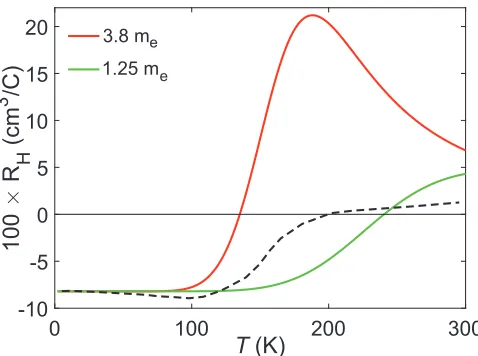
Sign-change of the Hall coefficient
Our model also gives insight into the Hall effect in TiSe2. A long-standing problem has been why the samples, known to ben-doped, show a crossover from a negative Hall coefficient at low temperatures to a positive value at room temperature [1,3,12]. As shown in Fig.5, we also find a sign-change of the Hall effect in our model without CDW order, where we use the standard two-carrier transport equations to calculate the Hall response in the low-field limit:
RH=
µ2hnh−µ2ene
|e|(µhnh+µene)2
(2)
Once again, the relevant physics is the freezing-out of hole like carriers; below∼100 K, there are no thermally activated holes, and the Hall effect reduces to the simple one carrier model,RH ≈ −1/Nd|e|. However, as the holes become ac-tivated, due to their relatively high mobility, they quickly be-come very relevant in the Hall effect. By room temperature, even thoughnh < ne due to the extrinsic electron doping, the Hall coefficient is positive due to the higher hole mobility. Similar logic can likely account for the positive Seebeck coef-ficient at high temperatures [1]. We note that the Hall effect is particularly sensitive to the relative mobilities of electrons and holes, and here our assumption that the holes and electrons have the same scattering rate may cause a greater discrepancy
0 100 200 300
T
(K)
-10 -5 0 5 10 15 20
100
R
H(cm
3
/C)
[image:5.612.55.562.53.191.2]3.8 me 1.25 me
[image:5.612.320.559.486.664.2]with the experimental data, compared with the resistivity sim-ulations. In Fig.5we also show a simulation with a lowerm∗e, which gives better agreement at higher temperatures, reflect-ing the fact that the ratio of mobilities in our simple model may not be optimal. In addition, using the simple two-carrier equations may not completely encode the fact that there is one hole and three electron bands in the model. Nonetheless, the qualitative agreement in the crossover behavior again adds va-lidity to our simplified model approach, and points again to the key role played by thermally-activated carriers.
The sign change of the Hall effect was reported to occur at 181 K [3]. This proximity toTCDW might naively suggest a connection with changes in the Fermi surface atTCDW. How-ever, our simulations show that a sign-change of the Hall ef-fect, somewhere between 100 and 300 K, is generically to be expected simply from thermal activation of hole-like carriers. A sign-change of the Hall coefficient, or any slope-change, therefore is not a good metric ofTCDW[22], due to the dom-inance of thermal population effects in the measurements.
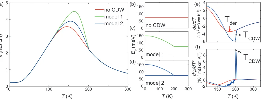
Effects of CDW order on resistivity
Having shown that the resistivity can be reasonably under-stood even without any CDW order, we now consider what effects the CDW could have on the transport properties. The CDW of TiSe2 significantly reconstructs the band structure, changes the effective masses of both the holes and the elec-tron bands, will have an impact on scattering rates, and more [4, 15]. Given the crude level of our model, it is not real-istic to attempt to simulate all of these effects, but we can gain some intuition on the possible effects of the CDW or-der with two simplified models. At TCDW, the hole bands hybridize across the band gap with the conduction bands. In the simplest case, therefore, one might consider simply
mod-ifying the band gap as Eg(T) = qE2
g0+ ∆(T)2, where
∆(T)takes an order-parameter-like form; we choose∆(T) =
∆0tanh (1.16
q TCDW
T −1)following Ref. [26]. This is en-coded by our model 1 in Fig.6, which is similar in spirit to the approach of Ref. [7]. AtTCDW, there is a change of slope below which resistance rises more rapidly than for the non-CDW case. Despite the large energy scale of the coupling (∆0 = 130 meV), however, the effects on the resistivity are not particularly dramatic: model 1 only moderately increases Tpeakand the absolute magnitude of the resistivity, while the overall shape remains similar.
Model 1 in fact overestimates the effects of the CDW. In fact, when the CDW occurs, the hybridization iskz-selective; the hole bands atΓhybridize strongly and get shifted to higher binding energies, while the hole bands at A are only weakly affected [15]. This idea is implemented in model 2, where we shift half of the density of states of the hole band belowTCDW according to the increased gap of model 1, but leave the other half at an unchanged energy. As one might expect, this has an even more muted effect on the total resistivity, with only a
weak change of slope atTCDW. This subtle deviation of the resistivity belowTCDW is consistent with the experimental changes in resistivity throughTCDW, where at most a modest change of slope is detected.
Neither of these simple models is even close to account-ing for all of the CDW physics, and in particular we do not consider any modifications to the electron bands through the transition. In fact, experimentally it is found that the elec-tron bands substantially change shape throughTCDW, and the conduction band minimum sinks to higher binding en-ergies, causing the band gap to actually be smaller in the CDW phase [15]. However, the most physically relevant pa-rameter is not the band gapper se, but the binding energy of the hole-like states, and especially in the case of model 2, these are reasonably consistent with the ARPES measure-ments. Thus, in the spirit of emphasizing the temperature-dependence of thermally-populated hole-like carriers, one can come to a qualitative understanding. Upon cooling the sam-ple, the CDW accelerates the freezing-out of hole-like car-riers as they are shifted to higher binding energy, increas-ing resistance below TCDW and bringing Tpeak to slightly higher temperatures; for example, model 2 increases Tpeak from 146 to 154 K. However, this freezing out of hole-like carriers would have happened even without the CDW order. We would therefore argue that, although the peak in resistiv-ity may be somewhat modulated by the CDW ordering, this is only a secondary effect. Fundamentally, there is no causal link between the peak in resistivity and the CDW, and the peak should primarily be understood it in terms of the thermal pop-ulation effects described earlier.
Criteria for the determination of CDW temperature
As in the simulations, a change of slope in resistivity mea-surements is a mark of the onset of CDW order, but in prac-tice a variety of procedures have been used in the literature to extractTc from experimental data. While the comparison of such criteria may seem a little mundane, the reliable deter-mination ofTc becomes crucial for the construction of phase diagrams based on tuning the properties of TiSe2. Supercon-ductivity has been found in TiSe2close to the critical point for the suppression of long-range CDW order via pressure [25], charge carrier doping [22], or intercalation [20,21,27]. How-ever, for a full understanding of the interplay of CDW and superconducting orders, it is important to be confident of the determination of the CDW phase boundary, which in some studies has been partially or solely delineated by the analy-sis of transport measurements. Thus there is a need to firmly establish the appropriate criterion for the determination ofTc from such measurements.
noth-0 50 100
Eg
(meV)
T (K) T (K)
0 1 2 3 4 5
no CDW model 1 model 2
-2 0 2 4 6
8
T
CDW -6
-4 -2 0 2 4
T
CDWT
der150
0 100 200 300
0 50 100 150
0 50 100 150
model 2 model 1 no CDW
T (K)
0 100 200 300 150 200 300
d
ρ
/dT
(10
-2 m
Ω
cm K
-1)
d
2ρ/dT
2
(10
-3 m
Ω
cm K
-2)
(a) (b)
(c)
(d)
(e)
(f)
ρ
(m
Ω
cm)
FIG. 6. (a) Resistivity curves, in which different approaches to the CDW are implemented below TCDW=202 K. (b-d) Corresponding temperature-dependence of the band gap in each case; in model 1 the band gap fully opens up, while in model 2 the hole DOS is split into two components belowTCDW, one of which doesn’t evolve with temperature. (e) Derivative of resistivity with respect to temperature, for model 2 and without CDW. Even without any CDW,dρ/dT shows a minimum atTder, which in this case is meaningless. (f) A sharp peak in the second derivative is the better indicator forTCDW.
ing is physically happening at this temperature. Moreover, in the simulations including CDW order, the minimum ofdρ/dT does not coincide withTCDW. The minimum of dρ/dT is therefore not an appropriate criterion. A more physical ap-proach is to look for a discontinuity in dρ/dT, since this should jump across TCDW [1]. While our simulations sup-port this idea in principle, in practice it may be difficult to precisely identify the midpoint of the step-like feature in the first derivative, given there is a substantially varying back-ground. Taguchiet al.[3], and more recently Campbellet al.
[14], argued that looking for a small but sharp peak in the sec-ond derivative is a better criterion for determiningTCDW. In agreement with this, our analysis presented Fig.6(f) shows a sharp peak centred atTcin the second derivative, although we note that discerning this peak in practice may often be com-plicated by the amplification of experimental noise in such second derivative analysis. Identifying the CDW onset tem-perature in TiSe2may, in general, therefore require additional measurements such as specific heat [2], or the observation of superlattice reflections in scattering measurements [31].
Discussion
In our simulations, the resistivity in the low temperature limit is always metallic-like (dρ/dT >0). For experimental samples grown by iodine vapor transport this is also usually the case, with the electron carriers coming from a finite ex-trinsic carrier density Nd. Experimentally, this arises from crystal imperfections: Se vacancies, intercalation of excess Ti, and residual iodine inclusions [18]. Correspondingly, a coherent electron-like Fermi surface is observed by ARPES at low temperatures [15], and there is a small but finite
Som-merfeld term in specific heat [2]. Such samples typically show an approximately constant Hall coefficient below 100 K [1], indicating thatNddoes not change significantly down to low temperature.
However, different methods of extrinsic doping lead to strongly varying results. For example Ti1−xTaxSe2 shows metallic-like behavior withdρ/dT > 0and a superconduct-ing dome, but Ti1−xNbxSe2gives insulating-likedρ/dT <0 all the way to room temperature [6,21], even though the Nb and Ta dopants are nominally isoelectronic. The details of how the dopant species interacts with the host matrix are thus highly relevant, as Nb dopants appear to cause substantially more disorder than Ta [21]. In other cases, such as lightly-doped PdxTiSe2[27] and some of the pressure-grown TiSe2 samples reported by Campbellet al.[14], the resistivity shows similar behavior to the iodine vapor transport-grown samples, with a slope-change atTcand a broad peak, but then exhibits a steep upturn in resistivity below 80-100 K, while the Hall coefficient only saturates at a much lower temperature, and at a larger magnitude [14]. This may reflect a significant fraction of the donated electrons becoming localized at low tempera-tures. Indeed, Moyaet al.[32] have recently shown evidence for weak localisation in iodine-free polycrystalline samples very close to stoichiometry. We note thatNd is treated as a constant in our simulations, and so no such upturn of the re-sistivity is found.
To our knowledge, there has been no successful synthesis of p-type TiSe2: all reported samples have a negative Hall coefficient at low temperatures, despite efforts by Levyet al.
[image:7.612.61.561.51.243.2]Much of the more recent literature on TiSe2has addressed the question of whether it is a semiconductor or semimetal, especially in the normal state [4,8,13,24,33–35]. Here, we have shown that the presence of a narrow band gap can natu-rally account for the overall form of the resistivity including the broad peak. In combination with recent high-resolution photoemission [15], this provides compelling evidence in fa-vor of a narrow band gap scenario.
In conclusion, we have shown that a minimal model based on the normal-state electronic structure of TiSe2can qualita-tively reproduce its known temperature-dependent transport behavior. Starting from the assumption of a narrow band gap, a crucial component is the temperature-dependence of the hole and electron carrier densities. Without incorporating any CDW-related changes, the broad peak in resistivity can be reproduced, and a sign-change in the Hall effect is also found. Thus neither of these experimental signatures is directly re-lated to the CDW. We included CDW order into the model with crude approximations, and showed that, despite large en-ergy scales being involved, the effect on resistivity was rela-tively muted, qualitarela-tively accounting for the typically weak signatures observed in transport at Tc. While the CDW in TiSe2 remains a highly interesting problem, our simple but robust simulations show that there is another effect which is more relevant for the overall understanding of the transport data of TiSe2, which is the thermal activation of mobile hole-like carriers.
ACKNOWLEDGMENTS
We thank K. Rossnagel for useful discussions, and all the authors of Ref. [15] who contributed to the photoemission data shown in Fig. 1. We gratefully acknowledge support from The Leverhulme Trust (Grant No. RL-2016-006) and The Royal Society. A.B. acknowledges support from The Physics Trust and the Student Staff Council of the School of Physics and Astronomy, University of St Andrews.
∗
†
[1] F. J. Di Salvo, D. E. Moncton, and J. V. Waszczak, “Electronic properties and superlattice formation in the semimetalTiSe2,”
Phys. Rev. B14, 4321–4328 (1976).
[2] R.A. Craven, F.J. Di Salvo, and F.S.L. Hsu, “Mechanisms for the 200 K transition inTiSe2: A measurement of the specific
heat,”Solid State Communications25, 39 – 42 (1978). [3] I. Taguchi, M. Asai, Y. Watanabe, and M. Oka, “Transport
properties of iodine-free TiSe2,”Physica B+C105, 146 – 150
(1981).
[4] K Rossnagel, “On the origin of charge-density waves in select layered transition-metal dichalcogenides,” Journal of Physics: Condensed Matter23, 213001 (2011).
[5] F. J. Di Salvo and J. V. Waszczak, “Transport properties and the phase transition inTi1−xMxSe2(M = Ta or V),”Phys. Rev.
B17, 3801–3807 (1978).
[6] F Levy, “The influence of impurities on the electrical proper-ties of TiSe2single crystals,”Journal of Physics C: Solid State
Physics13, 2901 (1980).
[7] C. Monney, H. Cercellier, C. Battaglia, E.F. Schwier, C. Didiot, M.G. Garnier, H. Beck, and P. Aebi, “Temperature dependence of the excitonic insulator phase model in 1T-TiSe2,”Physica B:
Condensed Matter404, 3172 – 3175 (2009).
[8] C. Monney, E. F. Schwier, M. G. Garnier, N. Mariotti, C. Did-iot, H. Beck, P. Aebi, H. Cercellier, J. Marcus, C. Battaglia, H. Berger, and A. N. Titov, “Temperature-dependent photoe-mission on1T-TiSe2: Interpretation within the exciton
conden-sate phase model,”Phys. Rev. B81, 155104 (2010).
[9] C Monney, E F Schwier, M G Garnier, N Mariotti, C Didiot, H Cercellier, J Marcus, H Berger, A N Titov, H Beck, and P Aebi, “Probing the exciton condensate phase in 1T-TiSe2with
photoemission,”New Journal of Physics12, 125019 (2010). [10] S. Koley, M. S. Laad, N. S. Vidhyadhiraja, and A. Taraphder,
“Preformed excitons, orbital selectivity, and charge density wave order in1T−TiSe2,”Phys. Rev. B90, 115146 (2014).
[11] B. Hildebrand, T. Jaouen, C. Didiot, E. Razzoli, G. Monney, M.-L. Mottas, A. Ubaldini, H. Berger, C. Barreteau, H. Beck, D. R. Bowler, and P. Aebi, “Short-range phase coherence and origin of the1T −TiSe2charge density wave,”Phys. Rev. B 93, 125140 (2016).
[12] J. A. Wilson, “Modelling the contrasting semimetallic charac-ters of TiS2 and TiSe2,” physica status solidi (b) 86, 11–36
(1978).
[13] K. Rossnagel, L. Kipp, and M. Skibowski, “Charge-density-wave phase transition in 1T −TiSe2 :Excitonic insulator
versus band-type Jahn-Teller mechanism,” Phys. Rev. B 65, 235101 (2002).
[14] D. J. Campbell, C. Eckberg, P. Y. Zavalij, and J. Paglione, “In-trinsic Insulating Ground State in Transition Metal Dichalco-genide TiSe2,”arXiv:1809.09467 (2018).
[15] Matthew D. Watson, Oliver J. Clark, Federico Mazzola, Igor Markovi´c, Veronika Sunko, Timur K. Kim, Kai Rossnagel, and Philip D. C. King, “Orbital- andkz-Selective Hybridization of Se4pand Ti3dStates in the Charge Density Wave Phase of TiSe2,”Phys. Rev. Lett.122, 076404 (2019).
[16] Philip B. Allen and N. Chetty, “TiTe2: Inconsistency between
transport properties and photoemission results,”Phys. Rev. B 50, 14855–14859 (1994).
[17] We compare our resistivity simulations with the sample grown at 575 C in Di Salvo 1976, and our Hall effect simulations with the data in the same reference on a sample grown at 600 C. [18] B. Hildebrand, C. Didiot, A. M. Novello, G. Monney,
A. Scarfato, A. Ubaldini, H. Berger, D. R. Bowler, C. Renner, and P. Aebi, “Doping Nature of Native Defects in1T−TiSe2,”
Phys. Rev. Lett.112, 197001 (2014).
[19] S. H. Huang, G. J. Shu, Woei Wu Pai, H. L. Liu, and F. C. Chou, “Tunable Se vacancy defects and the unconventional charge density wave in1T−TiSe2−δ,”Phys. Rev. B95, 045310 (2017).
[20] E. Morosan, H. W. Zandbergen, B. S. Dennis, J. W. G. Bos, Y. Onose, T. Klimczuk, A. P. Ramirez, N. P. Ong, and R. J. Cava, “Superconductivity in CuxTiSe2,”Nature Physics2, 544
(2006).
[21] Huixia Luo, Weiwei Xie, Jing Tao, Ivo Pletikosic, Tonica Valla, Girija S. Sahasrabudhe, Gavin Osterhoudt, Erin Sut-ton, Kenneth S. Burch, Elizabeth M. Seibel, Jason W. Krizan, Yimei Zhu, and Robert J. Cava, “Differences in Chemical Doping Matter: Superconductivity in Ti1−xTaxSe2but Not in
[22] L. J. Li, E. C. T. O’Farrell, K. P. Loh, G. Eda, B. ¨Ozyilmaz, and A. H. Castro Neto, “Controlling many-body states by the electric-field effect in a two-dimensional material,”Nature529, 185 (2015).
[23] Note that in Fig.3(a) the impurity scattering rate is held con-stant for all carrier densities, although experimentally it is likely to scale inversely withNe.
[24] K. Velebit, P. Popˇcevi´c, I. Batisti´c, M. Eichler, H. Berger, L. Forr´o, M. Dressel, N. Bariˇsi´c, and E. Tutiˇs, “Scattering-dominated high-temperature phase of1T−TiSe2: An optical
conductivity study,”Phys. Rev. B94, 075105 (2016).
[25] A. F. Kusmartseva, B. Sipos, H. Berger, L. Forr´o, and E. Tutiˇs, “Pressure Induced Superconductivity in Pristine 1T−TiSe2,”
Phys. Rev. Lett.103, 236401 (2009).
[26] P. Chen, Y.-H. Chan, X.-Y. Fang, Y. Zhang, M. Y. Chou, S.-K. Mo, Z. Hussain, A.-V. Fedorov, and T.-C. Chiang, “Charge density wave transition in single-layer titanium diselenide,” Na-ture Communications6, 8943 (2015).
[27] E. Morosan, K. E. Wagner, Liang L. Zhao, Y. Hor, A. J. Williams, J. Tao, Y. Zhu, and R. J. Cava, “Multiple electronic transitions and superconductivity in PdxTiSe2,” Phys. Rev. B 81, 094524 (2010).
[28] A. Wegner, J. Zhao, J. Li, J. Yang, A. A. Anikin, G. Kara-petrov, D. Louca, and U. Chatterjee, “Evidence for breathing-type pseudo Jahn-Teller distortions in the charge density wave phase of 1T-TiSe2,”arXiv: 1807.05664 (2018).
[29] John-Paul Castellan, Stephan Rosenkranz, Ray Osborn, Qing’an Li, K. E. Gray, X. Luo, U. Welp, Goran Karapetrov, J. P. C. Ruff, and Jasper van Wezel, “Chiral Phase Transition
in Charge Ordered1T−TiSe2,”Phys. Rev. Lett.110, 196404
(2013).
[30] L. J. Li, W. J. Zhao, B. Liu, T. H. Ren, G. Eda, and K. P. Loh, “Enhancing charge-density-wave order in 1T-TiSe2 nanosheet by encapsulation with hexagonal boron
nitride,” Applied Physics Letters 109, 141902 (2016), https://doi.org/10.1063/1.4963885.
[31] A. Kogar, G. A. de la Pena, Sangjun Lee, Y. Fang, S. X.-L. Sun, D. B. Lioi, G. Karapetrov, K. D. Finkelstein, J. P. C. Ruff, P. Ab-bamonte, and S. Rosenkranz, “Observation of a Charge Den-sity Wave Incommensuration Near the Superconducting Dome inCuxTiSe2,”Phys. Rev. Lett.118, 027002 (2017).
[32] Jaime M. Moya, C. L. Huang, Jesse Choe, Gelu Costin, Matthew S. Foster, and E. Morosan, “Weak-localization ef-fects reveals intrinsic semiconductor ground state in iodine-free-TiSe2,”arXiv:1903.12375 (2019).
[33] G. Li, W. Z. Hu, D. Qian, D. Hsieh, M. Z. Hasan, E. Morosan, R. J. Cava, and N. L. Wang, “Semimetal-to-Semimetal Charge Density Wave Transition in1T−TiSe2,”Phys. Rev. Lett.99,
027404 (2007).
[34] Matthias M. May, Christine Brabetz, Christoph Janowitz, and Recardo Manzke, “Charge-Density-Wave Phase of1T−TiSe2:
The Influence of Conduction Band Population,”Phys. Rev. Lett. 107, 176405 (2011).
![FIG. 1. Model band structure of TiSe2. (a) ARPES data at 300 K, adapted from [15], overlaid with parabolas corresponding to the assumeddispersions of the hole and electron-like carriers respectively](https://thumb-us.123doks.com/thumbv2/123dok_us/8983008.394668/2.612.71.561.52.173/structure-overlaid-parabolas-corresponding-assumeddispersions-electron-carriers-respectively.webp)