of Solid Oxide Fuel Cell Cathodes
Thesis by
Robert Ezra Usiskin
In Partial Fulfillment of the Requirements for the Degree of Doctor of Philosophy
CALIFORNIA INSTITUTE OF TECHNOLOGY
Pasadena, California
2015
© 2015
Acknowledgments
I owe thanks to a number of collaborators who made important contributions to
this work. Shingo Maruyama prepared several initial samples for the scanning
impedance probe. Chris Kucharczyk turned my Matlab data reduction routine from
a functional tool into a tour de force. Tim Fister and Kee-‐Chul Chang at Argonne
National Laboratory provided invaluable support for the synchrotron
measurements. Richard Wang helped with the SCN measurements.
I'm grateful to the Resnick Sustainability Institute at Caltech for the fellowship they
provided me and for the many interesting people they helped bring together.
Additional funding was provided by the National Science Foundation, the
California Institute of Technology Summer Undergraduate Research Fellowship
program, and the National Central University of Taiwan.
Many thanks to my research advisor Sossina Haile for sharing her scientific talent
and judgment and for being such an eminently reasonable advisor. Northwestern
will be lucky to have you.
I dedicate this thesis to my parents, Zalman and Karen Usiskin. This work would
never have happened without their devotion and support and the high value they
Abstract
In the first half of this thesis, a new robotic instrument called a scanning impedance probe is presented that can acquire electrochemical impedance spectra in automated fashion from hundreds of thin film microelectrodes with systematically
varied properties. Results from this instrument are presented for three catalyst
compositions that are commonly considered for use in state-‐of-‐the-‐art solid oxide
fuel cell cathodes. For (La0.8Sr0.2)0.95MnO3+δ (LSM), the impedance spectra are well
fit by a through-‐the-‐film reaction pathway. Transport rates are extracted, and the
surface activity towards oxygen reduction is found to be correlated with the
number of exposed grain boundary sites, suggesting that grain boundaries are
more surface-‐active than grains. For La0.5Sr0.5CoO3-‐δ (LSC), the surface activity
degrades ~50x initially and then stabilizes at a comparable activity to that of
previously measured Ba0.5Sr0.5Co0.8Fe0.2O3-‐δ films. For Sr0.06Nb0.06Bi1.87O3 (SNB), an
example of a doped bismuth oxide, the activity of the metal-‐SNB boundary is
measured.
In the second half of this thesis, SrCo0.9Nb0.1O3-‐δ is selected as a case study of
perovskites containing Sr and Co, which are the most active oxygen reduction
catalysts known. Several bulk properties are measured, and synchrotron data are
presented that provide strong evidence of substantial cobalt-‐oxygen covalency at
high temperatures. This covalent bonding may be the underlying source of the high
Table of Contents
CHAPTER 1 OVERVIEW ... 1
1.1 SUMMARY... 1
1.2 WHY STUDY SOLID OXIDE FUEL CELL (SOFC) MATERIALS?... 1
1.3 WHY STUDY THIN FILMS OF SOCF CATALYSTS?... 2
1.4 WHY STUDY BULK DEFECT CHEMISTRY?... 5
1.5 WHY FOCUS ON THE BULK DEFECT CHEMISTRY OF SRCO0.9NB0.1O3-‐Δ?... 7
CHAPTER 2 HIGH THROUGHPUT CHARACTERIZATION OF (La0.8Sr0.2)0.95MnO3+δ THIN FILM MICROELECTRODES... 8
2.1 INTRODUCTION... 8
2.2 OVERVIEW OF THE SCANNING IMPEDANCE PROBE... 11
2.3 EXPERIMENTAL PROCEDURES... 12
2.4 RESULTS OF PHYSICAL CHARACTERIZATION... 15
2.5 RESULTS OF ELECTROCHEMICAL CHARACTERIZATION... 20
2.6 DISCUSSION... 36
2.7 CONCLUSION... 38
CHAPTER 3 HIGH THROUGHPUT CHARACTERIZATION OF TWO OTHER MATERIAL SYSTEMS: La0.5Sr0.5CoO3+δ AND PLATINUM - Sr0.06Nb0.06Bi1.87O3...52
3.1 SUMMARY... 52
3.2 TWO MATERIAL SYSTEMS... 52
3.2.1 La0.5Sr0.5CoO3... 53
3.2.2 Sr0.06Nb0.06Bi1.87O3... 54
3.3.2 Film preparation... 56
3.3.3 Impedance characterization... 57
3.4 ELECTROCHEMICAL MODELS... 58
3.5 LA0.5SR0.5COO3 RESULTS... 60
3.5.1 Structural characterization... 60
3.5.2 Impedance data... 65
3.6 SR0.06NB0.06BI1.87O3 RESULTS... 73
3.6.1 Structural characterization... 73
3.6.2 Impedance spectra ... 74
3.7 CONCLUSIONS... 79
CHAPTER 4 MORE DETAIL ABOUT THE SCANNING IMPEDANCE PROBE...82
4.1 SUMMARY... 82
4.2 PARALLEL CHARACTERIZATION... 82
4.3 PARALLEL FABRICATION... 84
4.4 SCANNING IMPEDANCE PROBE: DETAILS... 88
4.4.1 Mechanical... 88
4.4.2 Thermal... 90
4.4.3 Gas Control ... 92
4.4.4 Electronic ... 93
4.4.5 Software... 93
4.5 SOME OBSTACLES TO OBTAINING GOOD DATA, AND HOW TO OVERCOME THEM... 94
4.5.1 Tip Cooling... 94
4.5.4 Contamination ... 99
4.5.5 Sheet resistance... 99
CHAPTER 5 BULK PROPERTIES OF SCN ...101
5.1 SUMMARY...101
5.2 WHY STUDY THE BULK DEFECT CHEMISTRY OF SRCO0.9NB0.1O3-‐Δ (SCN)? ...101
5.3 EXPERIMENTAL DETAILS...102
5.4 RESULTS AND DISCUSSION...104
5.5 CONCLUSIONS...115
CHAPTER 6 ELECTRONIC BEHAVIOR OF SrCo0.9Nb0.1O3-δ...117
6.1 SUMMARY...117
6.2 BACKGROUND...117
6.3 EXPERIMENTAL DETAILS...119
6.3.1 Synthesis ...119
6.3.2 Quenching ...120
6.3.3 Initial characterization...121
6.3.4 X-ray absorption spectroscopy ...121
6.3.5 Non-resonant inelastic x-ray scattering...122
6.4 RESULTS AND DISCUSSION...124
6.4.1 Quenching ...124
6.4.2 X-ray photoelectron spectra ...127
6.4.3 X-ray absorption fine structure ...128
6.4.4 Non-resonant inelastic x-ray scattering...132
List of Figures
FIGURE 2.1. SCHEMATIC OF THE TEST CONFIGURATION IN THE SCANNING IMPEDANCE PROBE. DIMENSIONS ARE NOT
TO SCALE. ...11
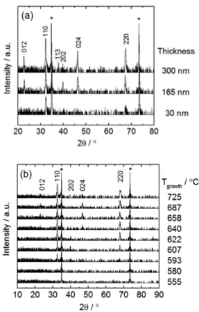
FIGURE 2.2. X-‐RAY DIFFRACTION PATTERNS ACQUIRED FROM VARIOUS REGIONS OF TWO (LA0.8SR0.2)0.95MNO3+Δ
THIN FILM LIBRARIES: (A) LIBRARY #1, 30 -‐ 300 NM THICKNESS, 650 ˚C GROWTH TEMPERATURE, 10 MTORR
O2 GROWTH PRESSURE, 1 HZ LASER PULSE RATE. (B) LIBRARY #3, 135 NM THICKNESS, 555 -‐ 725 ˚C
GROWTH TEMPERATURE, 30 MTORR O2 GROWTH PRESSURE, 5 HZ LASER PULSE RATE. THE ORIENTATION OF
EACH LSM REFLECTION IS INDICATED. REFLECTIONS MARKED WITH AN ASTERISK ARE FROM THE YSZ
SUBSTRATE...16
FIGURE 2.3. TYPICAL LIBRARY OF (LA0.8SR0.2)0.95MNO3+Δ THIN FILM MICROELECTRODES GROWN ON A 5 MM X 10
MM Y0.15ZR1.85O1.93 SUBSTRATE. LEFT: SCHEMATIC LAYOUT. RIGHT: OPTICAL PHOTO OF LIBRARY #1 DURING
IMPEDANCE MEASUREMENTS...17
FIGURE 2.4. ATOMIC FORCE MICROGRAPHS ACQUIRED AFTER PATTERNING FROM A THICKNESS LIBRARY OF
(LA0.8SR0.2)0.95MNO3+Δ MICROELECTRODES (LIBRARY #1, UNIFORM 650 ˚C GROWTH TEMPERATURE). THE
CORRESPONDING THICKNESS AND ROOT-‐MEAN-‐SQUARED ROUGHNESS ARE LISTED UNDER EACH MICROGRAPH.
...18
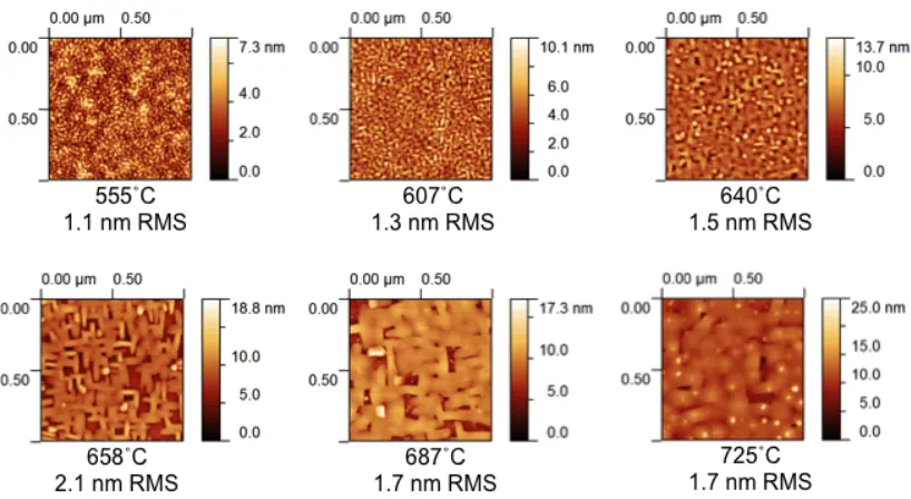
FIGURE 2.5. ATOMIC FORCE MICROGRAPHS ACQUIRED AFTER PATTERNING FROM A GROWTH TEMPERATURE LIBRARY
OF (LA0.8SR0.2)0.95MNO3+Δ MICROELECTRODES (LIBRARY #3, UNIFORM 135 NM THICKNESS). THE
CORRESPONDING GROWTH TEMPERATURE AND ROOT-‐MEAN-‐SQUARED ROUGHNESS ARE LISTED UNDER EACH
MICROGRAPH. ...19
FIGURE 2.6. FIB-‐SEM CROSS-‐SECTION ACQUIRED FROM A GROWTH TEMPERATURE LIBRARY OF
(LA0.8SR0.2)0.95MNO3+Δ FILMS (LIBRARY #3) AFTER IMPEDANCE TESTING. THE SAMPLE WAS COATED WITH
CONDUCTIVE AND PROTECTIVE LAYERS OF CARBON AND PLATINUM PRIOR TO FIB MILLING TO FACILITATE
IMAGING. THIS IMAGE WAS ACQUIRED USING A TILT ANGLE OF 52˚ OFF NORMAL. ...20
FIGURE 2.9. TYPICAL IMPEDANCE SPECTRA (A), ZOOMED VIEW OF THE SAME SPECTRA (B), AND GAIN/PHASE PLOTS
(C, D) PLOTS ACQUIRED FROM (LA0.8SR0.2)0.95MNO3+Δ MICROELECTRODES. SPECIFIC PARAMETERS FOR THESE
SPECTRA: LIBRARY #1, 200 ΜM DIAMETER, 192 NM THICKNESS, MEASURED AT ~710 ˚C OVER THE
FREQUENCY RANGE 10 KHZ -‐ 32 MHZ. FOR THE 1 ATM O2 DATA, THE RESULTS FROM A FULL 7-‐PARAMETER
FIT TO EQUATION 1 (DASHED RED LINE) AND A 6-‐PARAMETER FIT HOLDING RION FIXED (SOLID BLACK LINE)
ARE SHOWN; THEY FALL SO CLOSELY ON TOP OF EACH OTHER IN THESE PLOTS AS TO BE INDISTINGUISHABLE.
...24
FIGURE 2.10. (A) IMPEDANCE SPECTRA MEASURED AT ~710 ˚C AND 0.01 ATM O2 FROM LA0.8SR0.2)0.95MNO3+Δ
MICROELECTRODES OF VARIOUS THICKNESSES IN LIBRARY #1. (B) ZOOMED VIEW OF A SUBSET OF THE SAME
SPECTRA. ...25
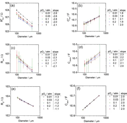
FIGURE 2.11. DIAMETER DEPENDENCE OF THE SIX FIT PARAMETERS MEASURED FROM A THICKNESS LIBRARY OF
(LA0.8SR0.2)0.95MNO3+Δ FILMS (LIBRARY #1) AT ~710 ˚C UNDER VARIOUS OXYGEN PARTIAL PRESSURES
WITH 246 NM MICROELECTRODE THICKNESS. THE LINES ARE LINEAR FITS, THE SLOPES OF WHICH ARE
INDICATED NEXT TO THE LEGEND. 95% CONFIDENCE INTERVALS FROM THE FITS ARE SHOWN, EXCEPT WHERE
THEY ARE SMALLER THAN THE DATA POINTS...27
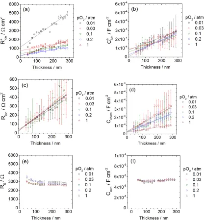
FIGURE 2.12. THICKNESS DEPENDENCE OF THE SIX FIT PARAMETERS MEASURED FROM A THICKNESS LIBRARY OF
(LA0.8SR0.2)0.95MNO3+Δ FILMS, LIBRARY #1, AT ~710 ˚C AND THE INDICATED OXYGEN PARTIAL PRESSURES.
WHEN FITTING THE SPECTRA ACQUIRED UNDER 0.2 ATM O2 AND 1 ATM O2, RION WAS HELD FIXED AT THE
VALUE DETERMINED BY AVERAGING THE RION VALUES OBTAINED FROM THE FITS TO IMPEDANCE SPECTRA
ACQUIRED FROM THE SAME MICROELECTRODE AT 0.01 ATM O2, 0.03 ATM O2, AND 0.1 ATM O2. 95%
CONFIDENCE INTERVALS FOR THE FITS ARE SHOWN, EXCEPT WHERE THEY ARE SMALLER THAN THE DATA
POINTS. ...30
FIGURE 2.13. AMBIPOLAR DIFFUSIVITY DCHEM (LEFT) AND VOLUME-‐NORMALIZED CHEMICAL CAPACITANCE CCHEM
(RIGHT) OF (LA0.8SR0.2)0.95MNO3+Δ AT ~710 ˚C. THE ORANGE BOX BOUNDS THE RANGE OF VALUES FOR DCHEM
PREVIOUSLY MEASURED FROM BULK SAMPLES OF LA0.8SR0.2MNO3+Δ.29 COMPARABLE LITERATURE DATA IS
(LA0.8SR0.2)0.95MNO3+Δ LIBRARY UNDER 0.2 ATM O2, ~710 ˚C, 200 ΜM DIAMETER ELECTRODES, OVER THE
FREQUENCY RANGE 10 KHZ -‐ 32 MHZ. POINTS ARE RAW DATA, CURVES ARE FITS TO EQUATION 1. ...33
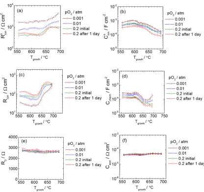
FIGURE 2.15. FIT PARAMETERS MEASURED FROM THE GROWTH TEMPERATURE LIBRARY OF (LA0.8SR0.2)0.95MNO3+Δ
FILMS, LIBRARY #3, AT ~710 ˚C AND THE INDICATED PO2. THE MICROELECTRODE DIMENSIONS WERE 200
ΜM DIAMETER AND 135 NM THICKNESS THROUGHOUT. LINES CONNECT THE POINTS AS GUIDES FOR THE EYE.
95% CONFIDENCE INTERVALS ARE SHOWN, EXCEPT WHERE THEY ARE SMALLER THAN THE DATA POINTS...34
FIGURE 2.16. ELECTROCHEMICAL ACTIVITY MEASURED AT ~710 ˚C UNDER 0.01 ATM O2 FROM LIBRARIES OF
(LA0.8SR0.2)0.95MNO3+Δ MICROELECTRODES WITH 200 ΜM DIAMETER AND VARIOUS GROWTH TEMPERATURE
(BLUE SQUARES, 10 MTORR O2 GROWTH) OR VARIOUS THICKNESSES (ORANGE, TRIANGLES AND CIRCLES ARE
SAMPLES GROWN IN 30 MTORR O2 AND 10 MTORR O2, RESPECTIVELY). ...36
FIGURE S17. PRIMARY CHAMBER OF THE SCANNING IMPEDANCE PROBE. LEFT: EXTERNAL PHOTO. RIGHT: COMPUTER
MODEL CROSS-‐SECTION SHOWING THE CHAMBER INTERIOR. ...40
FIGURE S18. OPTICAL PHOTO OF THE STAGE USED TO ASYMMETRICALLY HEAT SUBSTRATES DURING PREPARATION
OF THE LIBRARY OF GROWTH TEMPERATURES...40
FIGURE S19. SEEBECK VOLTAGE MEASURED BETWEEN THE COUNTER ELECTRODE AND AN OXIDE MICROELECTRODE
CONTACTED BY A PALINEY7 PROBE TIP. RESCALING THE VOLTAGE BY THE SEEBECK COEFFICIENT OF YSZ
YIELDS AN ESTIMATE FOR THE ASSOCIATED TEMPERATURE DROP BETWEEN THE ELECTRODES, ALSO SHOWN.
CURVES ARE POWER-‐LAW FITS TO THE DATA AT EACH TEMPERATURE...42
FIGURE S20. XRD PATTERNS ACQUIRED FROM A THICKNESS LIBRARY OF (LA0.8SR0.2)0.95MNO3+Δ
MICROELECTRODES, LIBRARY #2, GROWN AT 650 ˚C UNDER 10 MTORR O2. THE CORRESPONDING FILM
THICKNESS IS LISTED TO THE RIGHT OF EACH PATTERN. THE ORIENTATION OF EACH LSM REFLECTION IS ALSO
INDICATED. REFLECTIONS MARKED WITH AN ASTERISK ARE FROM THE YSZ SUBSTRATE. ...44
FIGURE S21. LEFT: TYPICAL ROCKING CURVE ACQUIRED FROM THE (LA0.8SR0.2)0.95MNO3+Δ GROWTH TEMPERATURE
LIBRARY IN A REGION WHERE TGROWTH = 725 ˚C. THE TWO FIT COMPONENTS ARE SHOWN IN RED AT BOTTOM;
THE FIT RESIDUAL IS SHOWN IN GREEN AT TOP. RIGHT: FULL WIDTH AT HALF MAXIMUM (FWHM) VALUES
LIBRARY OF (LA0.8SR0.2)0.95MNO3+Δ MICROELECTRODES GROWN AT 650 ˚C UNDER 10 MTORR O2. THE
CORRESPONDING FILM THICKNESS AND ROOT-‐MEAN-‐SQUARED ROUGHNESS ARE LISTED UNDER EACH
MICROGRAPH. ...45
FIGURE S23. SEM IMAGES FROM THE (LA0.8SR0.2)0.95MNO3+Δ GROWTH TEMPERATURE LIBRARY AFTER EXPOSURE
FOR 2 DAYS AT ~710 ˚C IN THE SCANNING IMPEDANCE PROBE. SOME OF THE OBSERVED CONTRAST IS DUE TO
MILD SAMPLE CHARGING...46
FIGURE S24. EXPONENT OF THE CONSTANT PHASE ELEMENT USED TO REPRESENT THE SURFACE CAPACITANCE
(CIONS) WHEN FITTING IMPEDANCE SPECTRA ACQUIRED FROM THE THICKNESS LIBRARY AT ~710 ˚C, 200 ΜM
DIAMETER TO THE MODEL SHOWN IN EQUATION 1. 95% CONFIDENCE INTERVALS ARE SHOWN...47
FIGURE S25. THICKNESS DEPENDENCE OF THE FIT PARAMETER RION MEASURED FROM THE (LA0.8SR0.2)0.95MNO3+Δ
THICKNESS LIBRARY AT ~710 ˚C AT VARIOUS OXYGEN PARTIAL PRESSURES. THIS PLOT IS IDENTICAL TO THE
PLOT OF RION IN FIGURE 2.12, EXCEPT HERE ALL SEVEN PARAMETERS WERE FREE TO VARY IN ALL FITS,
INCLUDING THE 0.2 ATM AND 1 ATM FITS. 95% CONFIDENCE INTERVALS ARE SHOWN...47
FIGURE S26. THICKNESS DEPENDENCE OF THE AMBIPOLAR DIFFUSIVITY DCHEM CALCULATED FROM THE
(LA0.8SR0.2)0.95MNO3+Δ THICKNESS TRENDS SHOWN IN FIGURE 2.12 FOR ~710 ˚C. 95% CONFIDENCE
INTERVALS ARE SHOWN. (THEY ARE ARTIFICIALLY SMALL FOR THE 0.2 ATM AND 1 ATM ISOBARS, SINCE RION
WAS HELD FIXED IN THOSE FITS.)...48
FIGURE S27. TYPICAL IMAGES USED TO ESTIMATE THE SURFACE GRAIN BOUNDARY LENGTH. FILMS GROWN AT TWO
DIFFERENT TEMPERATURES ARE SHOWN. LEFT: AFM MICROGRAPHS. RIGHT: SAME MICROGRAPHS AFTER
IMAGE PROCESSING. THE SURFACE GRAIN BOUNDARY LENGTH WAS ESTIMATED BY SUMMING THE LENGTH OF
THE BORDERS BETWEEN THE GREEN REGIONS...49
FIGURE S28. SURFACE ROUGHNESS AND OUT-‐OF-‐PLANE (110) PLANE SPACING MEASURED FROM THE AS-‐GROWN
(LA0.8SR0.2)0.95MNO3+Δ TEMPERATURE LIBRARY USING AFM, XRD, AND AFM, RESPECTIVELY. ...49
FIGURE S29. SURFACE GRAIN BOUNDARY LENGTH ESTIMATED USING AFM IMAGES FROM THE GROWTH
TEMPERATURE LIBRARY (BLUE) AND TWO THICKNESS LIBRARIES GROWN AT 10 MTORR O2 (CIRCLES) AND 30
THIS PARTICULAR PROFILE WAS ACQUIRED FROM AN 80 ΜM DIAMETER MICROELECTRODE IN LIBRARY #1..50
FIGURE S31. SURFACE RESISTANCE RIONS EXTRACTED FROM IMPEDANCE SPECTRA AT 710 ˚C IN 0.2 ATM O2 USING
200 ΜM DIAMETER MICROELECTRODES FROM TWO THICKNESS-‐GRADIENT LIBRARIES GROWN ON DIFFERENT
SUBSTRATES AND MEASURED SEPARATELY. 95% CONFIDENCE INTERVALS ARE SHOWN. LINES ARE LINEAR
FITS. ...51
FIGURE 3.1. POSSIBLE ELECTROCHEMICAL PATHWAYS. (A) MIXED CONDUCTING PELLET, (B) MIXED CONDUCTING
MICROELECTRODE, (C) ELECTRONICALLY CONDUCTING MICROELECTRODE WITH SURFACE DIFFUSION ON
ELECTROLYTE, AND (D) ELECTRONICALLY CONDUCTING MICROELECTRODE WITH ELECTRON MIGRATION
THROUGH ELECTROLYTE...59
FIGURE 3.2. EQUIVALENT CIRCUITS FOR (A) MIXED CONDUCTING PELLET, (B) LA0.5SR0.5COO3 MICROELECTRODE, (C)
(LA0.8SR0.2)0.95MNO3 MICROELECTRODE, AND (D) PT MICROELECTRODE ON SR0.06NB0.06BI1.87O3...59
FIGURE 3.3. XRD PATTERNS ACQUIRED FROM A SINGLE YSZ SUBSTRATE CONTAINING LA0.5SR0.5COO3 FILMS WITH
THICKNESSES IN THE RANGE 30 NM -‐ 300 NM. COURTESY OF SHINGO MARUYAMA...60
FIGURE 3.4 LA0.5SR0.5COO3-‐δ FILMS AS GROWN BY PLD WITH THICKNESSES OF 30 NM (UPPER LEFT), 84 NM (UPPER
RIGHT), LOWER LEFT (192 NM), AND LOWER RIGHT (300 NM). COURTESY OF SHINGO MARUYAMA. ...61
FIGURE 3.5. OPTICAL PHOTOS OF TYPICAL LSC SAMPLES. FROM LEFT TO RIGHT: VARIOUS THICKNESSES RANGING
FROM 300 NM -‐ 30 NM; A SAMPLE CONTAINING EXACTLY TWO FILM THICKNESSES, 300 NM AND 30 NM; AND
UNIFORM 200 NM THICKNESS. SOME DARK SMUDGES ARE VISIBLE; THIS IS RESIDUAL SILVER PASTE ON THE
BACKSIDE OF THE TRANSPARENT SUBSTRATE (USED TO AFFIX THE SUBSTRATE DURING DEPOSITION)...61
FIGURE 3.6. AFM PROFILE SCAN OF AN LSC MICROELECTRODE WITH 300 NM NOMINAL THICKNESS, 30 UM
NOMINAL DIAMETER. COURTESY OF SHINGO MARUYAMA...62
FIGURE 3.7. EDGE QUALITY OF LSC FILMS AFTER PATTERNING BY ION MILLING. LEFT: SEM MICROGRAPH, TAKEN
FROM A SAMPLE WITHOUT CARBON COATING. RIGHT: AFM PROFILE SCAN, COURTESY OF SHINGO MARUYAMA.
LA0.5SR0.5COO3-‐δ FILM WITH 100 NM THICKNESS THAT DID NOT UNDERGO IMPEDANCE TESTING. SAMPLE IS
TILTED 52˚ IN THE CENTER AND RIGHT IMAGES...64
FIGURE 3.9 SEM MICROGRAPHS ACQUIRED AFTER IMPEDANCE TESTING OF LA0.5SR0.5COO3-‐δ FILMS WITH
THICKNESSES OF 30 NM (LEFT), 165 NM (MIDDLE), AND 300 NM (RIGHT). ...64
FIGURE 3.10. TYPICAL IMPEDANCE SPECTRA ACQUIRED FROM THIN FILM LA0.5SR0.5COO3-‐δ MICROELECTRODES OVER
THE FREQUENCY RANGE 10 KHZ -‐ 20 MHZ. POINTS ARE THE RAW DATA; CURVES ARE FITS TO THE
EQUIVALENT CIRCUIT SHOWN IN SECTION 3.4. THE DATA SHOWN HERE WERE ACQUIRED FROM
MICROELECTRODES WITH 200 ΜM DIAMETER AT THE INDICATED TEMPERATURES AND OXYGEN PARTIAL
PRESSURE. ...65
FIGURE 3.11. OFFSET RESISTANCE R0 EXTRACTED FROM IMPEDANCE SPECTRA MEASURED FROM LA0.5SR0.5COO3-‐
δFILMS OF VARIOUS THICKNESSES AT THE INDICATED TEMPERATURES AND OXYGEN PARTIAL PRESSURES. ...66
FIGURE 3.12. SURFACE RESISTANCE RS EXTRACTED FROM IMPEDANCE SPECTRA MEASURED FROM LA0.5SR0.5COO3-‐ δFILMS OF VARIOUS THICKNESSES AT THE INDICATED TEMPERATURES AND OXYGEN PARTIAL PRESSURES. ...67
FIGURE 3.13. TOTAL CAPACITANCE CCHEM EXTRACTED FROM IMPEDANCE SPECTRA MEASURED FROM LA0.5SR0.5COO3-‐
δFILMS OF VARIOUS THICKNESSES AT THE INDICATED TEMPERATURES AND OXYGEN PARTIAL PRESSURES. ...67
FIGURE 3.14. SURFACE RESISTANCE MEASURED ON A SECOND SAMPLE OF LSC MICROELECTRODES WITH
THICKNESSES OF 30 NM AND 300 NM, PROBED AT ~ 520˚C IN 0.01 ATM O2...68
FIGURE 3.15. AREA-‐NORMALIZED SURFACE RESISTANCE RS (UPPER LEFT), TOTAL CAPACITANCE CTOTAL (LOWER
LEFT), AND OFFSET RESISTANCE R0 (UPPER RIGHT) OF (200 ΜM DIAMETER) LA0.5SR0.5COO3-‐δ
MICROELECTRODES OF VARIOUS THICKNESSES AT 615˚C. LINES ARE LINEAR FITS TO THE RAW DATA POINTS.
THE FIT RESIDUALS ARE PLOTTED AS A SUBPLOT BELOW THE MAIN PLOT...70
FIGURE 3.16. COMPARISON OF THE VOLUME-‐NORMALIZED CHEMICAL CAPACITANCE OF THIN FILMS (THIS WORK)
AND BULK SAMPLES59 OF LA0.5SR0.5COO3-‐
δ. LINES CONNECTING THE DATA POINTS ARE GUIDES FOR THE EYE.
...72
FIGURE 3.17. SURFACE RESISTANCE RS OF LA0.5SR0.5COO3-‐δ FILMS AFTER DWELLING SEVERAL HOURS AT EACH GIVEN
MEASURED FROM SEVERAL FILM THICKNESSES. FOR COMPARISON, DATA AT 0.2 ATM FOR
BA0.5SR0.5CO0.8FE0.2O3-‐δ FILMS (GROWN ON SDC (100) ON YSZ (100)) ARE SHOWN AT RIGHT IN LIGHT GRAY
(FRANCISCO BARROSO, HAILE GROUP UNPUBLISHED)...72
FIGURE 3.18. OPTICAL (LEFT) AND SEM (RIGHT) IMAGES OF PLATINUM MICROELECTRODES ON AN SNB SUBSTRATE,
BEFORE IMPEDANCE TESTING. ...74
FIGURE 3.19. SEM IMAGES OF THE SNB SURFACE (LEFT) AND A PLATINUM MICROELECTRODE (RIGHT) AFTER
SEVERAL DAYS OF IMPEDANCE TESTING AT 575˚C -‐ 650˚C UNDER PO2 = 10-‐3 -‐ 1 ATM...74
FIGURE 3.20. IMPEDANCE SPECTRA ACQUIRED FROM PLATINUM MICROELECTRODES OF VARIOUS DIAMETERS ON
SNB AT ~ 625˚C IN 0.2 ATM O2. POINTS ARE RAW DATA; LINES ARE FITS TO THE EMPIRICAL EQUIVALENT
CIRCUIT DESCRIBED IN SECTION 3.4...75
FIGURE 3.21. OVERALL ARC WIDTH RDC-‐R0 (TOP) AND OFFSET RESISTANCE R0 (BOTTOM) MEASURED OVER TIME AT
THE INDICATED TEMPERATURES AND OXYGEN PARTIAL PRESSURES FROM PLATINUM MICROELECTRODES OF
VARIOUS DIAMETERS ON SNB. POINTS WERE EXTRACTED FROM THE IMPEDANCE SPECTRA; LINES CONNECT
THE POINTS AS GUIDES FOR THE EYE. ...76
FIGURE 3.22. OVERALL ARC WIDTH RDC-‐R0 MEASURED FROM PLATINUM MICRODOTS ON SNB AT ~625˚C AS A
FUNCTION OF DIAMETER (LEFT) AND OXYGEN PARTIAL PRESSURE (RIGHT). POINTS WERE EXTRACTED FROM
THE IMPEDANCE SPECTRA; LINES ARE LINEAR FITS ON A DOUBLE-‐LOGARITHMIC SCALE...77
FIGURE 3.23. ARRHENIUS PLOT OF THE ELECTROCHEMICAL REACTION RESISTANCE. THE FILM TEMPERATURES WERE
CORRECTED APPROXIMATELY FOR TIP COOLING. POINTS ARE EXTRACTED FROM THE IMPEDANCE SPECTRA;
LINES ARE LINEAR FITS TO THE POINTS. THE ACTIVATION ENTHALPY EXTRACTED FROM THE LINE SLOPES IS
SHOWN BESIDE THE LEGEND...79
FIGURE 4.1. SCHEMATIC OF THE TEST CONFIGURATION IN THE SCANNING IMPEDANCE PROBE. ...83
FIGURE 4.2. EXAMPLE LAYOUTS OF MICROELECTRODES ON A SAMPLE. LEFT: 17 X 21 = 357 MICROELECTRODES
(INCLUDING 11 DIFFERENT DIAMETERS) ON A 5 MM X 10 MM SUBSTRATE. RIGHT: 23 X 23 = 529
AND/OR COLUMNS OF A MICROELECTRODE ARRAY. ...86
FIGURE 4.4. SCHEMATIC OF A QUATERNARY LIBRARY THAT COULD BE MADE FROM FOUR BINARY TARGETS (BAFEOX,
SRFEOX, BACOOX, AND SRCOOX) TO SPAN THE FAMILY OF COMPOSITIONS BA1-‐XSRXCO1-‐YFEYO3-‐Δ, WHERE X,Y ε
[0,1]. ...88
FIGURE 4.5. SCANNING IMPEDANCE PROBE SYSTEM. ...89
FIGURE 4.6. PRIMARY CHAMBER OF THE SCANNING IMPEDANCE PROBE. LEFT: EXTERNAL PHOTO. RIGHT: COMPUTER
MODEL CROSS-‐SECTION, SHOWING THE CHAMBER INTERIOR. ...89
FIGURE 4.7. TYPICAL SAMPLE CONFIGURATIONS INSIDE THE SCANNING IMPEDANCE PROBE. LEFT: AT ROOM
TEMPERATURE WITH ADDED ILLUMINATION. RIGHT: A DIFFERENT SAMPLE AT ~800˚C SAMPLE
TEMPERATURE WITH NO ADDED ILLUMINATION. ...90
FIGURE 4.8. CALIBRATION OF THE SAMPLE SURFACE TEMPERATURE. LEFT: MEASUREMENT CONFIGURATION. RIGHT:
MEASURED "FILM" TEMPERATURE PLOTTED VS. THE STAGE (A.K.A. ELEMENT) TEMPERATURE. ...92
FIGURE 4.9. MEASURED VOLTAGE DROP VFILM -‐ VCOUNTER ELECTRODE ACROSS THE YSZ SUBSTRATE USING AN
LA0.5SR0.5COO3-‐D MICROELECTRODE AND A TIP MADE OF PALINEY7 (A NOBLE METAL ALLOY CONTAINING
PRIMARILY PALLADIUM)...95
FIGURE 4.10. LEFT: SPURIOUS INDUCTANCE AT HIGH FREQUENCIES, CAUSED BY IMPROPER CHOICE OF CURRENT
RANGE. RIGHT: SPURIOUS JUMP IN THE DATA UPON CHANGING CURRENT RANGES FOR LOW CAPACITANCE
SAMPLES...98
FIGURE 5.1. X-‐RAY POWDER DIFFRACTION PATTERNS FOR SCN AFTER CALCINATION AT 1200˚C (RED), AFTER A
SUBSEQUENT ANNEAL AT 750˚C IN AIR FOR 10 D (GREEN), AND AFTER A SUBSEQUENT ADDITIONAL ANNEAL
AT 1200˚C IN AIR FOR 10 H (BLUE). ... 105
FIGURE 5.2. OXYGEN STOICHIOMETRY 3-‐Δ OF BSCF AND SCN MEASURED BY THERMOGRAVIMETRY, PLOTTED FOR COMPARISON WITH DATA FROM OTHER REPORTS ON LA0.1SR0.9CO0.8FE0.2O3-‐Δ (LSCF 1982)70,
SRCO0.8FE0.2O3-‐Δ (SCF 082)71, SCN72, AND BSCF63,67,69... 106
ISOTHERMS, AND (D) SCN ISOBARS, PLOTTED WITH COMPARABLE LITERATURE DATA.72,73... 109
FIGURE 5.5. ELECTRONIC CONDUCTIVITY Σ OF BSCF AND SCN PLOTTED AS ISO-‐STOICHIOMETRIC CURVES. LINES
CONNECT THE DATA POINTS AS GUIDES FOR THE EYE. ... 111
FIGURE 5.6. LATTICE PARAMETER A0 OF EQUILIBRATED SCN MEASURED BY IN SITU X-‐RAY DIFFRACTION. CURVES
SHOWN ARE LINEAR FITS TO THE DATA. ALSO PLOTTED ARE COMPARABLE LITERATURE DATA FOR
EQUILIBRATED BSCF TAKEN BY NEUTRON DIFFRACTION.68... 112
FIGURE 5.7. LATTICE PARAMETER A0 OF EQUILIBRATED SCN, PLOTTED AS A FUNCTION OF OXYGEN NON-‐
STOICHIOMETRY Δ. CURVES SHOWN ARE LINEAR FITS TO THE DATA. ERROR BARS FOR D ARE ESTIMATED AS
±0.10 (ABSOLUTE) AND ±0.02 (RELATIVE)... 113
FIGURE 5.8. LINEAR EXPANSIVITY AL OF SCN PLOTTED WITH COMPARABLE LITERATURE DATA FOR BSCF.68... 114
FIGURE 5.9. LINEAR CHEMICAL EXPANSIVITY AC OF SCN PLOTTED WITH COMPARABLE LITERATURE DATA FOR
BSCF.68... 115
FIGURE 6.1. SCHEMATIC OF THE BEAMPATH IN THE NRIXS EXPERIMENT. ... 122
FIGURE 6.2. THE LERIX SPECTROMETER USED IN THE NRIXS MEASUREMENTS AND LOCATED AT BEAMLINE 20-‐ID
AT THE ADVANCED PHOTON SOURCE. TOP: OVERALL CONFIGURATION. LEFT: MOUNTING OF THE HIGH-‐
TEMPERATURE CHAMBER DURING THE NRIXS MEASUREMENT. RIGHT: SCN POWDER COMPACT USED IN THE
MEASUREMENT, BEFORE INSTALLATION INTO THE HIGH-‐TEMPERATURE CHAMBER... 123
FIGURE 6.3. TYPICAL MASS PROFILE OF AN SCN PELLET EQUILIBRATED IN THE TGA AT HIGH TEMPERATURE AND
THEN QUENCHED. SEE PELLET #5 IN TABLE 6.1 FOR PROCESSING PARAMETERS... 125
FIGURE 6.4. XRD PATTERNS TAKEN FROM THE SIX PELLETS SHORTLY AFTER QUENCHING. A VERTICAL BLACK LINE
WAS ADDED AT 67˚ TO MAKE THE PEAK SHIFTS BETWEEN SPECTRA EASIER TO SEE... 127
FIGURE 6.5. X-‐RAY PHOTOELECTRON SPECTRA MEASURED FROM SCN QUENCHED PELLETS WITH VARIOUS OXYGEN
STOICHIOMETRIES 3-‐Δ, SHOWING THE NIOBIUM 3D3/2-‐5/2 PEAKS (LEFT) AND COBALT 2P1/2-‐3/2 PEAKS (RIGHT).
RIGHT) K EDGES FOR SCN PELLETS QUENCHED WITH VARIOUS OXYGEN STOICHIOMETRIES. INSET PLOTS SHOW
AN ENLARGED VIEW OF THE EDGES AT THRESHOLD... 130
FIGURE 6.7. QUASI-‐CUBIC LATTICE PARAMETER A0 AND COBALT K EDGE THRESHOLD ENERGY AS A FUNCTION OF
OXYGEN STOICHIOMETRY... 131
FIGURE 6.8. OXYGEN K EDGES TAKEN BY NON-‐RESONANT INELASTIC X-‐RAY SCATTERING (NRIXS) ON SCN. DATA
INDICATED BY CIRCLES ARE A REPEAT RUN. ... 133
FIGURE 6.9. COBALT K EDGES FOR SCN TAKEN USING XAFS. GREEN = QUENCHED PELLET AT 25˚C WITH 3-‐Δ OF
2.55, RED = QUENCHED POWDER AT 25˚C WITH 3-‐ΔOF 2.57, PURPLE/BLUE = POWDER COMPACT
EQUILIBRATED AT 1000˚C WITH 3-‐Δ OF 2.45... 135
FIGURE 6.10. OXYGEN K EDGES ACQUIRED FROM LA0.6SR0.4FEO3-‐Δ BY NON-‐RESONANT INELASTIC X-‐RAY SCATTERING
(NRIXS). OXYGEN STOICHIOMETRIES LISTED IN THE LEGEND WERE CALCULATED FROM LITERATURE DATA86
AND IN-‐HOUSE THERMOGRAVIMETRY... 138
FIGURE 6.11. 57FE MÖSSBAUER SPECTRUM FROM LA0.6SR0.4FEO2.98 POWDER AT 25˚C. ... 138
List of Tables
CHAPTER 1 OVERVIEW
1.1 Summary
This thesis is divided into two halves. The first half describes a high throughput
approach for characterizing the electrochemical activity of thin film samples of solid oxide fuel cell (SOFC) catalysts. The second half contains investigations of
bulk samples that yield insight into the defect chemistry and electronic behavior of a model catalyst, SrCo0.9Nb0.1O3-‐δ (SCN). The two halves are linked by a common
motivation to understand the electrochemical properties of the most important
SOFC cathode materials. This motivation is explained below in more detail.
1.2 Why study solid oxide fuel cell (SOFC) materials?
Solid oxide fuel cells (SOFCs) are the most efficient devices yet invented for
converting fuel into electricity. Industrial systems that cogenerate electricity and
heat using SOFCs have projected efficiencies of up to ~75%, exceeding what is
possible in combustion systems.1 SOFC systems are also fuel flexible; they can
generate electricity from natural gas, hydrogen, ethanol, propane, biofuels, and
more. Furthermore, when operated in reverse, SOFCs are the most efficient
electrolyzers known, i.e., when supplied with electricity, an SOFC can efficiently
split water to generate hydrogen fuel. Despite the enormous promise of this
technology, commercial SOFC development has been hampered by inadequate
be improved. These technological capabilities and challenges are described in
detail elsewhere.1,2
The study of SOFC electrodes is also intricately linked to a number of fundamental
scientific questions in catalysis: What intrinsic material parameters determine the
rate of electrochemical charge transfer at an interface? What are the reaction
pathways? What chemical changes cause catalysts to improve or degrade with
time? These questions have been discussed in recent reviews pertaining to SOFC
cathode3-‐5 and SOFC anode5,6 materials. Among other conclusions, these reviews
make clear the importance of electrochemical impedance measurements on dense
patterned thin film electrodes for elucidating the redox activity and catalytic
pathways at the surfaces of these materials.
1.3 Why study thin films of SOCF catalysts?
The motivation for measuring dense patterned thin films is that in porous catalyst
microstructures, a consequence of porosity is that the intrinsic surface activity of
the catalyst is convoluted with extrinsic factors like surface area, microstructure
interconnectedness, tortuosity, length of the so-‐called "triple phase boundary" (the
boundary between the catalyst, the electrolyte, and the gas phase, where the rate-‐
limiting step is often thought to occur), and so on. It can be quite difficult to
characterize and deconvolute these geometry-‐dependent factors. The task has
been helped by recent advances in 3D characterization techniques like x-‐ray
microscopy. However, these methods remain fairly slow and expensive and often
include significant uncertainty. On the other hand, by using dense samples with well-‐characterized geometries, it becomes easier to normalize by geometry (e.g.,
scaling catalytic activity by surface area) to obtain intrinsic material properties.
A second common difficulty is that in typical electrochemical methods for
measuring activity (which involve current and voltage measurements and which
go by various names, including a.c. impedance spectroscopy and d.c. voltammetry),
it is challenging to decoupling the rates of the anode and cathode reactions, since
they occur simultaneously and both contribute to the overall measurement. In
electrochemical systems with a liquid electrolyte, this common problem is usually resolved by using a reference electrode, i.e., a third electrode that is placed in the
liquid electrolyte to help decouple the potential changes at the two electrodes.
Numerous workers have also tried to use a reference electrode to decouple the
anode and cathode overpotentials in systems with a solid electrolyte. However, papers by Adler and others have shown quantitatively that "minor errors in the
alignment of the anode and cathode can create significant errors in the measured
half-‐cell overpotential... [including] cross-‐contamination of anode and cathode
frequency response... [and] even if electrodes are perfectly aligned, differences [in
kinetics]... may cause inherent distortion of the impedance, including frequency
dispersion and inductive artifacts."7 For this reason, reference electrodes have
As an alternative, microelectrodes have emerged over the last fifteen years as a
reference-‐less way to decouple the anode and cathode behavior. In this approach,
the two electrodes are fabricated with vastly different surface areas: a small area
working electrode (~ 10-‐4 cm2) is dwarfed by a large area counter electrode (~ 1
cm2). In such a configuration, the measured electrochemical response can often be
attributed entirely to the small area electrode, a.k.a. the microelectrode, with
negligible error. The conditions under which this attribution is sufficiently
accurate have been estimated previously.8
These sample requirements -‐-‐-‐ dense, geometrically well-‐defined, and having tiny
area -‐-‐-‐ motivate the use of patterned thin film microelectrodes. First reported in
2000,9 such films are typically grown by physical vapor deposition (usually pulsed
laser deposition or sputtering) and then patterned into the desired shapes by
photolithography and subsequent dry etching (milling with argon ions) or wet
etching (dissolution in acid). The area/perimeter of the microelectrodes can be
systematically varied within a single pattern, which helps to identify scaling
relations and interpret the electrochemical results. Roughly 25 papers using this
approach have been published since 2000.
Despite its success, a number of issues have constrained the microelectrode
approach. First, sample preparation is slowed by the need to synthesize a different
hundreds of compositions can thus be quite cumbersome. (This constraint is not
unique to the microelectrode approach.) Varying other parameters besides
composition -‐-‐-‐ film thickness, surface decoration, growth conditions, substrate
orientation, and so on -‐-‐-‐ has also required growing numerous films one at a time,
in series. Acquiring impedance spectra from these samples also had to be done in
series, further adding to the experiment time. This time constraint likely explains
why studies typically report results for only two or three film thicknesses, even in
cases where film thickness appears to be a critical parameter.10,11 Another issue is
that subtle differences between samples prepared or characterized in series can
introduce experimental errors that mask trends of interest. Surface activity may be
sensitive to small changes in impurity content, for example. Also, prior to this
work, the acquisition of each of hundreds or potentially thousands of impedance
spectra required the cumbersome operator task of manually contacting each
microelectrode with a tiny metal probe tip every few minutes. Perhaps in part
because of the repetitive nature of this task, the stability and repeatability of
impedance measurements from microelectrodes are not always clearly reported in
the literature. Indeed, sometimes the stability is not mentioned at all,10,11 leaving
the reader to assume(perhaps incorrectly) that the material properties are entirely
stable over time.
1.4 Why study bulk defect chemistry?
The surface activity is arguably the single most important property of a catalyst,
but there are many reasons why understanding the bulk defect chemistry may also
be extremely useful:
First, bulk thermodynamic instability of a material can explain why its surface
properties change with time. Second, correlations between surface and bulk
transport rates (specifically, the oxygen tracer surface exchange coefficient k* and
the oxygen tracer bulk diffusion coefficient D*) have been observed over a wide
range of oxygen-‐conducting materials,12,13 suggesting that the surface and bulk
properties are closely linked. Third, in SrTi1-‐xFexO3-‐δ a strong correlation has been
observed between the surface activity and the Fermi level in bulk samples, again
suggesting that the surface catalystis and the bulk electronic structure can be
closely linked.14 Fourth, a knowledge of bulk properties helps with experimental
design. For example, the results of thin film studies of surface activity can be
distorted if electronic sheet resistance contributes significantly to the measured
impedance, and knowing the electronic conductivity helps in predicting and
avoiding this distortion.15 Fifth, a knowledge of bulk properties also helps with
device fabrication. For example, a nearly ubiquitous concern in developing
practical solid oxide fuel cell devices is that if the thermochemical expansivities of
the cathode and electrolyte are not well-‐matched, mechanical stresses can crack
the electrolyte and ruin the device.
1.5 Why focus on the bulk defect chemistry of SrCo0.9Nb0.1O3-δ?
As described further in Section 3.2, a large number of state-‐of-‐the-‐art SOFC
cathode catalysts are materials with the perovskite structure that contain the
elements Sr and Co. This category of materials includes such compositions as
Ba0.5Sr0.5Co0.8Fe0.2O3-‐δ (BSCF), La1-‐xSrxCo1-‐yFeyO3-‐δ (LSCF), La1-‐xSrCoO3-‐δ (LSC),
SmxSr1-‐xCoO3 (SSC), and others. The composition SrCo0.9Nb0.1O3-‐δ (SCN)16 also
exhibits extraordinary performance as a fuel cell cathode,17 yet its defect chemistry
is likely simpler than many of the above compositions, since it contains only three
cations, and the niobium cation is in relatively low concentration and is fixed-‐
valent (as shown in Chapter 6).18 For these reasons SCN is a reasonable choice as a
"model material" for fundamental studies of persovskites containing Sr and Co;
thus SCN is the focus of the bulk defect chemistry investigations in Chapter 5 and
Chapter 6.
CHAPTER 2 HIGH THROUGHPUT CHARACTERIZATION OF
(La0.8Sr0.2)0.95MnO3+δ THIN FILM MICROELECTRODES
This chapter introduces the scanning impedance probe, a robotic instrument that
can rapidly measure the electrochemical impedance response of hundreds of thin
film electrodes in automated fashion. This instrument is combined with a parallel
fabrication method that produces libraries containing hundreds of thin film
electrodes with systematically varied properties on a single substrate. Results are
presented from libraries of (La0.8Sr0.2)0.95MnO3+δ (LSM) microelectrodes with
systematically varied area, thickness, and growth temperature. The measured
impedance spectra are well fit by a physically derived electrochemical model, and
all trends are consistent with a pathway involving oxygen reduction over the
entire surface of the LSM microelectrode followed by diffusion through the film
and into the YSZ electrolyte. The surface activity is found to be correlated with the
number of exposed grain boundary sites, suggesting that grain boundaries are
more active than grains towards the rate-‐limiting surface process.
2.1 Introduction
As described in Chapter 1, in recent years many studies have probed patterned
thin film electrodes using electrochemical impedance spectroscopy to yield rich
including accurate measurements of the intrinsic surface activity of such materials
towards oxygen electro-‐reduction.5 This chapter builds on the success of the
patterned thin film electrode approach by adding two innovations that increase
throughput and reliability. First, a scanning impedance probe is described that can
perform data acquisition and processing with higher throughput. Second, libraries
of thin film microelectrodes with systematically varied film thickness or growth
temperature are fabricated and characterized on a single solid electrolyte
substrate. This parallel fabrication method helps to further improve throughput,
and it helps avoid unintended differences that can arise when samples are
prepared or measured in series. Such differences can mask trends with the
parameters of interest.
In the specific case of (La1-‐xSrx)1-‐yMnO3+δ, a heavily studied cathode material that is
commonly used in commercial applications,2,3 both patterned and unpatterned
thin film studies have reached agreement that the three phase boundary pathway,
wherein oxygen incorporation into the electrolyte occurs at the boundary of the
LSM, electrolyte, and gas phases, is not always dominant, but can be outcompeted
by a through-‐the-‐film pathway, wherein oxygen ions incorporate at the LSM
surface, diffuse through the LSM film, and then cross into the electrolyte.9,10,19,20
Moreover, the shapes of the impedance spectra reported in these studies are
broadly similar; the typical spectrum includes a high frequency feature that
with a characteristic resistance that scales approximately linearly with increasing
film thickness.
However, there is substantial disagreement in the interpretation of these spectra
and in the conclusions drawn about the rates of the surface and bulk steps. In light
of the thickness trends just described, several studies suggested that the high-‐
frequency feature corresponds to the surface incorporation process, and that the
low frequency semicircle corresponds to bulk diffusion through the film.20-‐22
However, these reports do not mention the possibility that surface properties (like
the number of exposed grain boundaries) may depend on thickness.
On the other hand, using fits by an equivalent circuit based on a physically derived
model for MIECs, Fleig et al. assigned the high frequency feature to bulk diffusion
and the low frequency semicircle to surface incorporation.10 These authors noted
that the resulting surface exchange rate increased somewhat with increasing
thickness, and they commented that there may be a "thickness-‐dependent film
structure and chemistry".
The present study seeks to resolve this disagreement, which is important because
of its direct implications for how to improve surface activity in an LSM-‐based
cathode. In particular, if the largest contribution to the electrode resistance comes
from surface incorporation, then modifying the LSM surface (e.g., by decoration
resistance contribution comes from diffusion through the film, then alternate
strategies would be more beneficial.
2.2 Overview of the scanning impedance probe
The configuration of the scanning impedance probe is shown schematically in
Figure 2.1 and to scale in Figure S17.
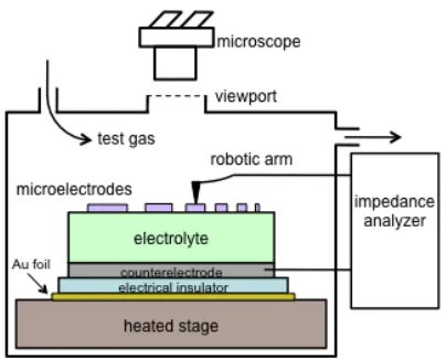
Figure 2.1. Schematic of the test configuration in the scanning impedance probe.
Dimensions are not to scale.
Compared to previously reported instruments for probing microelectrodes,9,23 the
most significant new feature here is the scanning capability: the position of the
alumina arm holding the metal probe tip is determined by three orthogonal lead
screws connected to stepper motors (Figure S17). Thus the metal probe tip can be
touched to a microelectrode simply by entering the coordinates of that
microelectrode in the control software. The temperature and gas environment are
the patterning process are small enough that the relative spacing of the
microelectrodes on the substrate surface can be accurately predicted, and three
points are sufficient to define the plane of that surface. Consequently, once the user
manually finds the coordinates of three reference microelectrodes in a library, the
coordinates of all the other microelectrodes can be readily computed. Hundreds of
microelectrodes can then be probed in any desired sequence over a range of
environmental conditions in automated fashion.
2.3 Experimental procedures
A sintered pellet of (La0.8Sr0.2)0.95MnO3 (LSM) was prepared for use as a pulsed
laser deposition target as follows. First, a dense compact was prepared from 20 g commercial powder (Fuel Cell Materials, 99.5% pure) with 1 wt% polyvinylpyrrolidone added to serve as a binder. The powder was subjected to uniaxial pressure under 20 MPa for 10 min in a 32 mm diameter die, followed by isostatic pressure under 350 MPa for 20 min. The edges and faces of this powder compact were shaved using a razor to remove any surface contamination from the die, then this powder compact was placed on an alumina support with excess powder spread below the compact to avoid reactivity with the alumina. The compact was then sintered at 1450 ˚C for 5 h in stagnant air in a dedicated alumina tube. The resulting pellet was polished on all sides with sandpaper down to 600 grit, sonicated in water and isopropanol to remove the residual grit, and finally measured as having 26 mm diameter and 6 mm thickness. X-‐ray diffraction (XRD, Philips X'Pert Pro, Cu Ka) patterns acquired from both faces of the pellet showed good agreement with patterns reported in the Inorganic Crystal Structure Database for a virtually identical composition (La0.8Sr0.2MnO3).
Using this target, (La0.8Sr0.2)0.95MnO3 films were grown on (100)-‐oriented single
crystal Y0.15Zr1.85O1.93 substrates (YSZ, 8 mol% Y2O3-‐stabilized ZrO2, 5 mm x 10 mm
x 0.5 mm, MTI Corporation) by pulsed laser deposition with a KrF excimer laser (248 nm, 0.8 J/cm2, 1 Hz). During film growth, each substrate was adhered to a
heated stage with silver paste, which was subsequently scraped off.
deposition parameters for Library #1 were as follows: 650 ˚C growth temperature, 10 mtorr O2 working pressure, 1 Hz ablation laser pulse frequency, 0.7 nm/min
deposition rate, and 100 ˚C/min cooling rate. For Library #2, all conditions were identical with the exception of the working pressure, which was held at 30 mtorr O2.
On a third substrate, the growth temperature of the LSM film was systematically varied using an asymmetric stage geometry (shown in Figure S18) heated at one end with infrared radiation. This procedure created a "growth temperature library", Library #3, in which the growth temperature varied continuously from 555 ˚C to 725 ˚C across the substrate. The substrate temperature was measured in numerous places during growth using an optical pyrometer. Other deposition parameters for Library #3 were as follows: uniform 135 nm thickness, 30 mtorr O2
pressure, 5 Hz ablation laser pulse frequency, 2.7 nm/min deposition rate (calibrated in advance by acquiring atomic force microscopy (AFM, Digital Instruments Nanoscope III) profiles from test films prepared with the same target and deposition parameters), and 20 ˚C/min cooling rate.
After growth, XRD patterns, rocking curves, and AFM micrographs were acquired from each film in several regions (Bruker D8 Discover, Cu Kα). Each film was then patterned into a library of microelectrodes using photolithography and ion milling. Specifically, two coats of photoresist (Shipley 1813) were applied by spin coating on top of each film, exposure to UV radiation through a photomask, and then development. The film then underwent ion milling for 45 min resulting in a milling depth of ~350 nm. The residual photoresist was then chemically stripped. In this way, each film was converted into a library of 337 circular microelectrodes. Each library included nine different values of microelectrode diameter spanning the range 50 μm -‐ 500 μm. The "growth temperature library" included twenty-‐one different values of growth temperature, unevenly spaced from 555 ˚C -‐ 725 ˚C, while the thickness libraries included twenty-‐one different values of film thickness, evenly spaced from 30 nm -‐ 300 nm. Because the thickness or growth temperature varied continuously across each library it also varied slightly across each microelectrode. However, the microelectrodes had small enough diameter that a single value of thickness or growth temperature (the local average value) could be assigned to each microelectrode with minimal loss of accuracy. Specifically, for Libraries #1 and #2 the difference in thickness across the largest microelectrode probed (500 μm) is 15 nm, while for Library #3 the difference in growth temperature across the largest microelectrode probed (200 μm) was ~ 5 ˚C.
air at 600 ˚C -‐ 700 ˚C for 1 h induced sintering of the paste into a porous counter electrode.
Thus prepared, Library #1 was installed in the scanning impedance probe and heated to a stage temperature of 750 ˚C, which corresponded to a microelectrode temperature during probing of ~710 ˚C. A more detailed discussion of the temperature calibration is given in the Supplemental Information. The oxygen partial pressure (pO2) in the chamber was varied over the range 10-‐3 atm -‐ 1 atm
by flowing bottled oxygen or oxygen-‐nitrogen mixtures through the chamber and then past a zirconia-‐based oxygen sensor (Setnag) housed in a quartz tube in a separate furnace. The pO2 was allowed to stabilize at each condition prior to the acquisition of impedance measurements; typical stabilization times were 0.5 h -‐ 3 h. The total pressure in the chamber was always 1 atm. The microelectrodes were contacted using a probe tip made of Paliney7, a commercial alloy containing 35% Pd, 30% Ag, 14% Cu, 10% Au, 10% Pt, 1% Zn (American Probe & Technologies, 20
µm tip radius). Several measurements were repeated using a probe tip made of
Pt0.7Ir0.3 (Moser, 10 µm tip radius); identical impedance results were obtained. The
former probe material was preferred because it did not scratch the microelectrodes.
Impedance spectra were acquired using a frequency response analyzer (Solartron Modulab) with an applied a.c. voltage of 30 mV, no applied d.c. bias, and a typical frequency range of 10 kHz -‐ 16 mHz. As described in the Supplemental Information, cooling of the sample by the probe tip generated a temperature drop between the electrodes that has an associated 5 mV -‐ 25 mV Seebeck voltage (with the exact value depending on the microelectrode diameter (Figure S19)), so in fact each impedance spectrum was effectively measured under 5 mV -‐ 25 mV anodic d.c. bias, which was verified to be negligibly small for this material system. The analyzer calibration was verified in advance by acquiring impedance spectra from test circuits containing precision megaohm resistors and nanofarad capacitors; fits to these spectra reproduced the resistance and capacitance values with < 3% error. Impedance spectra acquired from the LSM microelectrodes were fit by an expression first suggested by Fleig et al.10 and described in detail below.