© 2017 IJSRST | Volume 3 | Issue 6 | Print ISSN: 2395-6011 | Online ISSN: 2395-602X Themed Section: Science and Technology
Review of CMOS based XOR/XNORs using Systematic Cell Design
Methodology
Ashok Yadav
*1, Dr. Manish Jain
2*1Department of Electronics and Communication, RKDF Institute of Science & Technology, Bhopal, India [email protected]
2
Department of Electronics and Communication, RKDF Institute of Science & Technology, Bhopal, India [email protected]
ABSTRACT
The XOR and XNOR gates are the essential blocks of various digital arithmetic and logical units such as digital adder, digital parity generator/checker, digital comparator, and digital encryption processor. Many circuit topologies have been proposed till now of full adder and XOR/XNOR gate design that can be categorised in two categories. First one offers full swing output and second one offers partial swing output. The Systematic Cell Design Methodology is partial swing based logic design method which offers less delay and low power consumption at weak logic ‘0’ and logic ‘1’ generation at output. This paper concludes a partial swing and pass transistor based XOR/XNOR gate which gives less propagation delay and low power dissipation at a cost of poor driving capability as compared to existing full adder. In this work results are simulated at 1.2Volt and 130nm technology.
Keyword: Hybrid CMOS logic; XOR/XNOR gate; partial swing logic; full swing logic.
I.
INTRODUCTION
In digital integrated circuits as the technology is getting advanced and innovative day by day, power consumption and delay is also increasing dramatically; saving power is high in demand as it will reduce the overall cost for mobile computing and higher integration density as well as reduction in delay offers higher computation speed. But poor voltage swing offered at output of logic block misguides or malfunction the next stage.
With the explosive growth, the demand, and the popularity of portable electronic products, the designers are driven to strive for smaller silicon area, longer battery life, higher speed, and enhanced reliability is increases with technology scaling. As Technology scaling increases the transistor count and operating frequency, which push the market demand for more and more function in Integrated circuit. However scaling always increases leakage power dissipation. As channel length reduces which results in increase of power dissipation with respect to technology progresses. To reduce the power consumption different logic design techniques like CMOS complementary logic, Dynamic
CMOS, Pseudo NMOS, Dynamic CMOS, CMOS Domino logic, Cascade voltage switch logic (CVSL), Modified Domino logic, Pass Transistor Logic (PTL) have been proposed [1-3]. Power dissipation depend on device structure property like gate oxide thickness, channel length, doping profile etc. as they are due to different physical phenomena Although Static CMOS Logic has been the most popular design approach for the past three decades [4, 5]. By scaling down the feature size of MOSFET devices in nano-meter, the supply voltage should be scaled down to avoid hot- carrier effects in CMOS circuits. To enhance the speed of the CMOS circuits, threshold voltage of the circuits has to be scaled down.
frequency of dynamic XOR improves, dynamic power consumption becomes dominant that introduce heating problem as mentioned above. To overcome this problem, dynamic XOR gate proposed with minimum delay and smaller power consumption.
II.
PUBLISHED LITERATURE
The recently published novel work can be divided into two categories as they are extracted from the topic: 1) traditional three input XOR gate and 2) its operating methodologies. Cell design methodology (CDM) has been presented to design some limited functions, such as two-input XOR/XNOR and carry–inverse carry in the hybrid-CMOS style [5-7]. The predominant results persuade us to improve Cell Design Methodology (CDM) through two stages: 1) generating more complex functions and 2) rectifying some remaining flaws. The flaws in previously published CDM include containing some manual steps in the design flow and generating a large number of designs in which the predominant ones would be determined after the completion of simulations. Therefore, in the first stage, a three-input XOR/XNOR as one of the most complex and all-purpose three-input basic gates in arithmetic circuits have been chosen. If the efficiency of the circuits is confirmed in such a competitive environment, it can show the strength of the methodology. In the second stage, CDM is matured as systematic CDM (SCDM) in designing the three-input XOR/XNORs for the first time. It systematically generates elementary basic cell (EBC) using binary decision diagram (BDD), and wisely chooses circuit components based on a specific target. This takes place when the mentioned features are not considered in the CDM. Therefore, after the systematic generation, the SCDM considers circuit optimization based on our target in three steps: 1) wise selection of the basic cell; 2) wise selection of the amend mechanisms; and 3) transistor sizing. It should be noted that BDD can be utilized for EBC generation of other three-input functions. We consider the power-delay product (PDP) as the design target. It stands as a fair performance metric, precisely involving portable electronic system targets. The motivation to use this
The SCDM divides a circuit structure into a main structure and optimization-correction mechanisms. In the main structure, it considers features including the least number of transistors in critical path, fairly balanced outputs, being power ground- free, and symmetry. The mechanisms have the duty of completing the functionality of the circuits, avoiding any degradation on the output voltage, and increasing the
driving capability. The dynamic consumption
optimization comes from the fact of well-balanced propagation delay. This feature is advantageous for applications in which the skew between arriving signals is critical for proper operation, and for cascaded applications to reduce the chance of making glitches [8]. Power-ground-free main structure leads to power reduction.
The degradation in all output voltage swing can thus be
completely removed, which makes the design
sustainable in low VDD operations and low static power dissipation. The methodology has high flexibility in target and systematically considers it in the three design steps. This can lead to efficient circuits in terms of performance, power, power delay product, energy delay product, layout area.
six inputs (A, B, C and compliment of all three inputs) and two outputs (XOR and its compliment).
Figure 1 Three input XOR/XNOR using transmission gate(TG16T)[10]
Figure 2 Three input XOR/XNOR using transmission gate and mirror circuit (TGM16T)[10]
Figure 3 Three input XOR/XNOR using transmission gate and mirror circuit (TGM18T)[10]
III. RESULT ANALYSIS AND COMPARISON
To review the performance of three input XOR/XNOR gate, it is necessary to study the transient analysis and process variation. This comparison have been performed complete study using Hspice [11]. To investigate further several modules with complementary outputs of full
adders (FAs), TFA, Hernandez1, Hernandez2,
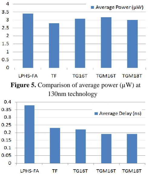
NEWHPSC, Hybrid, 18T_new_FS, and LPHS-FA have been analysed, whose excellence have been confirmed in [12] [13] and [14-16]. Therefore, an approximately fair comparison will take place by selecting them. Table-1 shows that TG16T[10], TGM16T[10] and TGM18T[10] technique have least PDP and delay than other existing conventional LPHS-FA and TF technique.
Figure 5. Comparison of average power (µW) at 130nm technology
Figure 6. Comparison of average delay (ns) at 130nm technology
Figure 7. Comparison of static power (µW) at 130nm technology
The comparison of Average PDP (fJ), Average Power (µW), Average Delay (ns) and Static Power (µW) are shown in Figure 4, Figure 5, Figure 6 and Figure 7 respectively. The layout area occupied by existing XOR/XNOR cells is shown in Table-1.
Table-1: Comparison of layout area at 130nm technology
Circuits Area(µm2)
LPHS-FA
NA (too
large)
TF 0.15
IV. CONCLUSION
Logic gate XOR/XNOR gates are frequently used in high performance data processing units. Logic gate with high speed gates, low power static power and low dynamic power are most demanded in modern integrated circuit. In recently published work TG16T, TGM16T and TGM18T offers smaller delay and low dynamic power consumption due to reduction no. of switching node but offers higher static power consumption due to transmission technology as compared to existing technique LPHS-FA and TG. We will improve this fault in future research work.
V.
REFERENCES
[1]. I. S. Abu-Khater, A. Bellaouar, and M. Elmasry, "Circuit techniques for CMOS low-power high-performance multipliers," IEEE Journal of solid-state circuits, vol. 31, pp. 1535-1546, 1996. [2]. U. Ko, T. Balsara, and W. Lee, "Low-power
design techniques for high-performance CMOS adders," IEEE Transactions on Very Large Scale Integration (VLSI) Systems, vol. 3, pp. 327-333, 1995.
[3]. A. Bellaouar and M. Elmasry, Low-power digital VLSI design: circuits and systems: Springer Science & Business Media, 2012.
[4]. A. M. Shams and M. A. Bayoumi, "A novel high-performance CMOS 1-bit full-adder cell," IEEE Transactions on circuits and systems II: Analog and digital signal processing, vol. 47, pp. 478-481, 2000.
[5]. D. Radhakrishnan, "Low-voltage low-power CMOS full adder," IEE Proceedings-Circuits, Devices and Systems, vol. 148, pp. 19-24, 2001. [6]. H. T. Bui, A. K. Al-Sheraidah, and Y. Wang,
"New 4-transistor XOR and XNOR designs," in ASICs, 2000. AP-ASIC 2000. Proceedings of the Second IEEE Asia Pacific Conference on, 2000, pp. 25-28.
[8]. H. Kaul, M. A. Anders, S. K. Mathew, S. K. Hsu, A. Agarwal, R. K. Krishnamurthy, et al., "A 320 mv 56 μw 411 gops/watt ultra-low voltage motion estimation accelerator in 65 nm cmos," IEEE Journal of Solid-State Circuits, vol. 44, pp. 107-114, 2009.
[9]. J.-M. Wang, S.-C. Fang, and W.-S. Feng, "New efficient designs for XOR and XNOR functions on the transistor level," IEEE Journal of solid-state Circuits, vol. 29, pp. 780-786, 1994.
[10]. T. Nikoubin, M. Grailoo, and C. Li, "Energy and Area Efficient Three-Input XOR/XNORs With Systematic Cell Design Methodology," IEEE Transactions on Very Large Scale Integration (VLSI) Systems, vol. 24, pp. 398-402, 2016. [11]. A. Eshra and A. El-Sayed, "An odd parity checker
prototype using DNAzyme finite state machine,"
IEEE/ACM Transactions on Computational
Biology and Bioinformatics, vol. 11, pp. 316-324, 2014.
[12]. C.-K. Tung, S.-H. Shieh, and C.-H. Cheng, "Low-power high-speed full adder for portable electronic applications," Electronics Letters, vol. 49, pp. 1063-1064, 2013.
[13]. M. Aguirre-Hernandez and M. Linares-Aranda, "CMOS full-adders for energy-efficient arithmetic applications," IEEE transactions on very large scale integration (VLSI) systems, vol. 19, pp. 718-721, 2011.
[14]. S. Goel, M. A. Elgamel, M. A. Bayoumi, and Y. Hanafy, "Design methodologies for high-performance noise-tolerant XOR-XNOR circuits," IEEE Transactions on Circuits and Systems I: Regular Papers, vol. 53, pp. 867-878, 2006. [15]. S. Goel, A. Kumar, and M. A. Bayoumi, "Design
of robust, energy-efficient full adders for deep-submicrometer design using hybrid-CMOS logic style," IEEE Transactions on Very Large Scale Integration (VLSI) Systems, vol. 14, pp. 1309-1321, 2006.
![Figure 2 Three input XOR/XNOR using transmission gate and mirror circuit (TGM16T)[10]](https://thumb-us.123doks.com/thumbv2/123dok_us/9108989.1445237/3.595.310.546.53.254/figure-input-xor-xnor-using-transmission-mirror-circuit.webp)