SRAM Interface and AHB-Lite
Interconnect Testing
K.Jamal*, Dr P. Srihari **, G. Kanakasri***
* Departement of Electronocs and Communication Engineering, GRIET, Hyderabad, India ** Departement of Electronocs and Communication Engineering, VNRVJIET, Hyderabad, India
***Departement of Electronocs and Communication Engineering, GRIET, Hyderabad, India
Abstract: The increase in the size of embedded memory for system-on-chip(SOC) and multicore processors has
a positive impact on performance yet an immense challenge is faced in terms of chip yield, power consumption, and overall cost. Now a days a major percentage (>than 60%) processors and SOC area in both 2-D (planar) and 3-D technologies, such as Through Silicon Via (TSV), are dedicated to memory. Most of the models of today’s embedded memories are not as simple as a storage area with single interface of data, address and control but rather they comprise of complex logic on their interface due to constraints in timing and interconnect technologies. Memory core testing strategy is well understood and has mature tools and methodologies to detect the defects such as Built-In-Self-Test (BIST). In addition, core and logic-based testing using scan and automatic test pattern generation tools and methodologies are used for flop based design. Yet, interface logic and complex interconnect like the one in 3-D chips are not thoroughly tested by using either by BIST or Automatic Test Pattern Generation as they are not designed for such logic. This becomes even more important for 3-D chips where a stack memory could have different testing strategies other than the base layer core which is interfacing with it. This presents a design for test methodology to reach good coverage on interface logic design for embedded and stack memory. The proposed approach uses AHB-Lite as interconnect and we use bypass logic to test both interface and interconnect.
Index Terms— Interface testing; Embedded memory; AHB-Lite; Flop based design; Interconnect testing
I INTRODUCTION
The increasing density of transistor per area provided by process technology scaling and recently by 3-D or through silicon via technology integration provides an opportunity to step-up embedded memory for SOC and multicore processors [2]. It is estimated that minimum 68% of typical System-On-Chip area will be dedicated to memory by 2017 as shown in Fig. 1[3]. Such increase in memory size coupled with the increase in process variation and voltage scaling creates a big challenge for memory yield [3]. Even though semiconductor companies do not publish any data regarding yield due to confidentiality, but, it is a well-known secret that for all digital System -On-Chip and multi-core, memory failures are big contributors for yielding losses.
Figure 1. Memory as a percentage of total die size [1]
time without impact on fault coverage or product quality. In this brief, we propose a Design For Testability (DFT) scheme that is compatible with industry standard tools aiming at increasing coverage on memory interface logic and interconnect. The proposed scheme is not only compatible with planar 2-D design, but it can be utilized for 3-D chip for interconnect testing. In this approach, we have used AHB-Lite as an interconnect.
This brief is organized as follows. Section II introduces AHB-Lite protocol, and operation. Section III summarizes the shortcomings of current testing approaches. Section IV proposes DFT scheme and its improvement on memory and interface coverage V results VI conclusion.
II AHB-Lite PROTOCOL AND ITS OPERATION
AMBA AHB-Lite [8] addresses the prerequisites of high-performance synthesizable circuits. It is a bus interface that supports a single bus master and it provides high-bandwidth operation.
AHB-Lite applies the features needed for high-performance, high clock frequency processors including: • Burst transfers of data
• Single-clock edge operation • Non-tri state implementation
• Wide data bus configurations like 64, 128, 256, 512, and 1024 bits.
The most commonly used AHB-Lite slaves are internal memory devices, external memory interfaces, and high bandwidth peripherals. Even though, low-bandwidth peripherals can be included as AHB-Lite slaves, for system performance reasons they typically reside on AMBA [8] Advanced Peripheral Bus (APB). The Bridging between this higher level of bus and APB is done by using a AHB-Lite slave known as APB bridge. Figure 2 shows a single master AHB-Lite system design with one AHB-Lite Master and two AHB-Lite Slaves. The AHB-Lite bus interconnect logic consists of one address decoder and a slave-to-master multiplexer. The main functionality of decoder is to monitor the address from the master so that the appropriate slave is selected and then the multiplexer routes the corresponding slave output data back to the master.
The main components of an AHB-Lite system are described in: • Master
• Slave • Decoder. • Multiplexer.
Figure 2. AHB-Lite block diagram
A. Operation
The master initiates a transfer by driving the address and controlling the signals. These signals provide information about the address, direction, width of the transfer, and indicates the transfer forms part of a burst. Transfers can be of the following types:
• Single
• Incrementing bursts that do not wrap at address boundaries • Wrapping bursts that wrap at particular address boundary limits.
The write data bus (HWDATA)[8] transfers data from the master to a slave, and the read data bus transfers data from the slave to the master. Every transfer must consist of: Address phase (one address and control cycle), and Data phase (one or more cycles for the data).
slave to gain extra time to provide or sample data. The slave uses HRESP (AHB Response)to indicate the success or failure of a transfer.
III CURRENT TESTING APPROACHES
This section discusses the main testing methodologies, and tools available for digital systems, and their suitability in testing embedded memory core, periphery, and interface.
A. Built-In Self-Test
Built-in Self-Test (BIST) is an effective and fastest way to test regular structures. BIST has been the golden standard for memory testing. It uses dedicated hardware engine that is implementing algorithm to test and stress memory [9]. The main features of BIST are that, it runs at high speed and requires small testing time. It can perform testing on multiple combinations of data and address to guarantee that the memory core is fully tested and is free of noise related problems. The basic principle of BIST depends on performing three functions: initially a WRITE operation of particular data patterns to a specific address in the memory. This operation followed by a READ operation to recall the written data. The next operation is to equate the written data with the currently READ data. As a result of testing, a pass or fail signature is generated after the completion of all BIST vectors are run. Another useful mode of BIST is effective in the debug mode, during this mode, the BIST identifies the exact failing address which can interface with other software tools to locate the exact location of the failing cells. Nevertheless, the disadvantage of BIST is that it impacts silicon area and timing. In addition to the requirement of having dedicated hardware for BIST engine for generating data patterns and result comparison at high speed, the routing resources from all memory interfaces to the BIST engine has a non-negligible cost. The main impact of BIST on functional timing is that all memory interface signals needs to be multiplexed between BIST signals and functional signals. In most cases, designers try to minimize this impact on chip timing by looking for a less critical timing stage to inject BIST data. Overall BIST is still important and provides a wide range coverage in testing the memory core with the basic address, data in, data out, READ, and WRITE control signals. However, BIST will not be able to deal some of the shadow logic that may be embedded in the memory interface logic (Figure. 3).
The memory model in Built In Self Test mode is the same as functional mode with the same RTL, gate level, and timing abstraction. Memory timing abstraction used for functional mode is also used during BIST simulation and verification. A major challenge in BIST mode is to minimize the effect of other components of the chip on the tested block. On one hand, it is significant to make sure that the rest of the chip, which is not referred to memory, does not memory functionality. On the other hand, the effect of injected noise on voltage supplies or memory related signals need to be considered. This is a source of discrepancy between functional and BIST mode. For example, a contention in logic, other than memory, would cause big power supply noise on the memory supply and may cause memory to fail, this could occur during BIST but not during functional mode.
B. Scan Design and Testing
There are two types of scan circuitry: 1) Internal scan and
2) Boundary scan.
Internal scan (also referred as scan design) is the internal change of design’s circuitry to increase its testability [4],[11]. Boundary scan adds scan circuitry around the periphery circuit of the block. That is to make the internal circuitry on the chip is accessible via a standard board interface. The added circuitry raises board testability of the chip, the chip I/O pads, and the interconnections of the chip to other board circuitry. Because the main focus of this brief is on embedded memory, only internal scan will be described as boundary scan and it can be applied only to stand-alone chips.
Scan-based testing methodology is combined with an ATPG CAD tools are effective testing methods for any flip-flop-based [5] digital design. Its durability comes from the fact that it translates a complex design with sequential elements to behave as combinational logic gates. Therefore, these gates’ models have been considered as state-of-the-art ATPG tools (such as Tmax), and have successfully detected faults with patterns which are generated from ATPG [12]. However, most processors and SoCs have a mixture of large and all memories, which are based on SRAMs, CAMs, ROMs, register-files, FIFOS, and many other regular structures. Even though the memory structure itself may be covered using other testing techniques like BIST, the periphery logic may not be tested with BIST.
Modeling of memory during ATPG differs from one design to another since it depends on the shadow logic that may exist and the memory interface. For example, a simple compiler memory or single ported custom SRAM-based memory has a minimum logic that is not covered by BIST. As such, during ATPG, this memory can be considered as a black box with no fault in memory during ATPG.
Figure 3. Block Diagram of Existing System [1]
Thus, a simple AND function of scan-mode and output of the memory insures that the output will be driven to a known value during ATPG and prevents X propagation. Another way for such modeling is to black box both of the core array and the sense amplifier. This approach tries to cover the glue logic around the array and the memory interface during ATPG. The X propagation is prevented through a complex logic added during test vector generation. All vectors that may result in READ before WRITE are marked as contention and get masked. Only vectors with a READ operation signal after a WRITE operation signal to the same address are allowed. This approach also requires sequential ATPG patterns. These patterns are complex and need special attention during ATPG mode.
C. Functional Testing
Functional testing is done by porting some of the high coverage tests used in verification phase of the design into test vectors. These tests are categorized as quality tests that focus on basic functionality of the design chip. The challenge in functional testing is in debugging failing tests. The failing point can be observed several cycles after the actual failure occurs. Even though the actual failure might not be identified, functional failure can give input to ATPG (scan)-based test to do further testing.
Since the functional test mode uses normal functional path, the functional model of memory is used and assert points can be identified from the RTL model. Because only few functional tests are run, the coverage to memory, interfaces, and glue logic is limited. In addition, the debugging of failures during functional mode can be challenging.
Traditionally, memory model for ATPG has been a black box where the WRITE-data-scannable flop, along with the control-signal flop, launch the data through the bypass path and not through the memory (Figure. 3). Then, they get sampled by the data output flop. As explained previously, SRAM-based memory array has only one operation each cycle, either READ or WRITE. This is true because the bit line and WL are shared between the two-operations.
In addition, in most design, the memory core gets blacked box and ATPG vectors stop at the boundary due to high cost, and added complexity (multi cycle ATPG patterns) of doing testing through the memory. The added complexity is due to the need for any READ operation to be preceded by a WRITE operation to the same address, otherwise the READ data will be unknown (X). Herein, the proposed approach seeks to change the memory array to do WRITE and READ in the same cycle throughtout ATPG. The complex multi cycle sequential patterns requirements to prevent x propagation will not be needed. From circuit point of view, the READ and WRITE operations can occur in the same cycle. Further, memory in this mode will pass the WRITE data into the output data through the memory bit line. As long as the WRITE driver is stronger than the bit cell, it will always direct the bit line to what the WRITE data value is. In addition, since the sense amplifier is triggered from the bit line value based on tracking circuitry [6], the result does not depend on the memory cell contents but rather it is determined by the WRITE data value. The memory core in this proposed scheme is behaving as a combinational circuit passing the WRITE data into output bus.
therefore, there is no special prerequisite needed on address bus. Also, the data input and output is the same as functional mode. The control signals will be modified accordingly to activate READ operation when WRITE operation is active, only during ATPG mode. The atpg_clk signal is OR-ed internally in the sub array to generate READ clock. As emphasized in previous Section, it is undesired to have an unknown data (X) out of the array. Thus, the READ operation is not allowed immediate WRITE is not asserted.
Most of the memory related BIST papers in the literature focus on optimizing BIST and memory repair. For example, Cao et al. focused on BIST in designing an efficient built-in self-repair strategy which can store each fault address only once. There are many challenges in 3-D chip testing [21] and this proposal can address some of the challenges especially testing the interconnect between the different chips.
One of the big advantages of utilizing ATPG for glue logic is that ATPG patterns are software generated and can be modified post silicon in which it does not add cost to hardware. In addition to the BIST hardware overhead and increased complexity, the memory interface still needs special attention during ATPG to prevent (X) propagation. The proposed method addresses this issue and the memory will be active during test mode. By this method we are testing simple interface and memory but we cannot test complex interfaces.
IV PROPOSED METHOD
Because of its high speed, high density, and its compatibility. The flop based 6T-SRAM cell is the preferred memory architecture for on-chip memory because of with CMOS logic process technology. In the proposed method AHB-Lite [8] is preferred to use as an interconnect. There are different types of interconnects available like AHB, ASB, APB. In this method, we are using AHB-Lite interconnect because it uses single master and multi slave. In this, masters can be any processing unit or CPU and the slaves can be internal memory devices or else external memory devices. In this memory and processing unit both are assumed as black boxes.
A. SRAM Operation
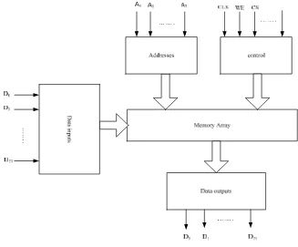
The main block is the memory core which consists of memory cells that are organized in 2-D arrays. The rest of the blocks are denoted to as periphery logic. The number of columns multiplied by the rows in the memory core gives the array size in bits. The 6T-SRAM cell is the preferred memory architecture for on-chip memory because of its high speed, high density, and compatibility with CMOS logic process technology. In addition, small signal swing on bit lines is desirable.
It is used in the majority of designs due to its unique properties, such as power efficiency and high utilization. Power efficiency is accomplished by using small voltage signals on the bit lines compared with full swing on other designs, while area utilization is incresed by increasing the number of rows in the same column [4]–[6]. The second block is a row decoder that is used to fully decode the encoded set address to select one set of Word Line (WL) from multiple rows. Consequently, the third block is the interface of data in, data out, and the sense amplifier which separates the memory core from the surrounding logic and restores full swing on data out.
Finally, the control part is the fourth block and is responsible for clock generation and enabling signal conditioning, such as READ enable, WRITE enable (wen), and test related signals or redundancy select signals [6], [7]. The simple functional mode operation of this array is a single WRITE or a READ operation in one cycle.. The block diagram of SRAM [22] operation is shown in fig 5.
Figure 5. Block diagram of SRAM operation
Initially, data will be generated by the processing unit. This data is fed as an input to AHB-Lite interface from that we acquire the data out as a output. We use bypass logic to test memory as well as complex interconnect. The bypass logic is placed in between interconnect and memory. We use mono control signal to test memory and interconnect. If control signal is high then it will test AHB-Lite interface. The output from interface is compared with input test pattern by using equality comparator. If output of the equality comparator is one then no error is present in the interface. Equality comparator is present inside the processing unit.
V RESULTS
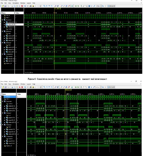
The simulation results for the proposed method are shown in figures 6, 7. In figure 6 the no error signal will become one when the processing unit input and memory don’t have any error. In this we have two memories. Out of these two memories the particular memory will be selected depending on hsel signal of interconnect.
If hsel1 is one, then memory1 output is selected for comparison. If hsel2 is one then memory 2 output is selected for comparison. The processing unit input is compared with particular memory output. This operation will be done when bypass logic enable is high.
If there is error in the interconnect then the no error signal will become zero as represented in figure 7. In this, we will compare interface data output with processing unit data input. These two are compared by using equality comparator. If these two-data outputs are not equal then we will get zero as output.
This operation will be done whenever bypass logic enable is high. The output of equality comparator is shown in the below figures to check whether there is an error in the interconnect or not.
VII CONCLUSION
This paper brief presented a methodology and DFT approach that can improve memory interface logic and interconnect fault coverage and hence it increases product quality.
The ATPG tool which is typically applied for flop-based design is used to test the memory interface logic and interconnect. The proposed approach employs bypass logic to test the AHB-Lite inter connect and memory interface.
Figure 6. Simulation results when no error is present in memory and interconnect
Figure 7. Simulation results whenever error present in the interconnect
REFERENCES
[1] Baker Mohammad “Embedded Memory Interface Logic and Interconnect Testing”, in IEEE Transactions On Very Large Scale Integration (VLSI) Systems, SEPTEMBER 2015.
[2] E. J. Marinissen and Y. Zorian, “Testing 3D chips containing throughsiliconvias,” in Proc. IEEE Int. Test Conf. (ITC), Nov. 2009, pp.
1–11.
[3] S. Kaushik and Y. Zorian. (Jul. 2012). Embedded Memory Test and Repair Optimizes SoC Yield. [Online]. Available:
http://www.eden.com
[4] B. Mohammad and H. Saleh, “Energy efficient and hign bandwidth embedded memory implementation,” in Proc. IEEE Design
Technol. Integr. Syst. (DTIS), Mar. 2013, pp. 117–121.
[5] N. H. E. Weste and D. M. Harris, CMOS VLSI Design: A Circuit and System Prospective, 4th ed. Reading, MA, USA:
Addison-Wesley, 2010.
[7] D. E. Khalil, M. Khellah, N.-S. Kim, Y. Ismail, T. Karnik, and V. K. De, “Accurate estimation of SRAM dynamic stability,” IEEE
Trans. VeryLarge Scale Integr. (VLSI) Syst., vol. 16, no. 12, pp. 1639–1647, Dec. 2008.
[8] AMBA 3 AHB-Lite Protocol v1.0 June. 2006
[9] Q. Chec, H. Mahmoodi, S. Bhunia, and K. Roy, “Efficient testing of SRAM with optimized March sequences and a novel DFT technique for emerging failures due to process variations,” IEEE Trans. VeryLarge Scale Integr. (VLSI) Syst., vol. 13, no. 11, pp.
1286–1295, Nov. 2005.
[10] B. Mohammad, N. Eleyan, G. Seok, and H. Kim, “Automated flow for generating CMOS custom memory bit map,” in Proc. IEEE
Int. DesignTest Symp. (IDTS), Dec. 2012, pp. 1–6.
[11] P. Nigh, “Scan-based testing: The only practical solution for testing ASIC/consumer products,” in Proc. Int. Test Conf. (ITC), 2002, p.
1198–1200.
[12] TetraMAX, Version E-2010.12-SP2, Synopsys Inc., Mountain View, CA, USA, 2010.
[13] G. Seok, B. Mohammad, and H. Kim, “Write-through method for embedded memory with compression Scan-based testing,” in Proc.
IEEE30th VLSI Test Symp., Apr. 2012, pp. 158 163.
[14] N. A. Touba, “Survey of test vector compression techniques,” IEEE Des.Test. Comput., vol. 23, no. 4, pp. 294–303, Apr. 2006.
[15] B. Mohammad,Embedded Memory Design for Multi-Core and SOC. New York, NY, USA: Springer-Verlag, Jan. 2014.
[16] Verplex, Version 6.1, Cadence Inc., Cranston, RI, USA, 2006.
[17] ESPCV, Version Y-2006.06-SP1, Synopsys Inc., Mountain View, CA, USA, 2006.
[18] S. Kundu, “GateMaker: A transistor to gate level model extractor for simulation, automatic test pattern generation and verification,” in
Proc.Int. Test Conf., Oct. 1998, pp. 372–381
[19] B. Mohammad, K. Lin, P. Bassett, and A. Aziz, “A 65 nm level-1 cache for mobile applications,” in Proc. IEEE ICM Conf., Sharjah,
UAE, Dec. 2008, pp. 5–10.
[20] S. Hamdioui, Z. Al-Ars, and A. J. van de Goor, “Opens and delay faults in CMOS RAM address decoders,” IEEE Trans. Comput.,
vol. 55, no. 12, pp. 1630–1639, Dec. 2006.
[21] M. Karunaratne and B. Oomann, “Optimizing BIST and repair logic for embedded memories,” in Proc. 51st MWSCAS, Aug. 2008,
pp. 350–353.n
![Figure 1. Memory as a percentage of total die size [1]](https://thumb-us.123doks.com/thumbv2/123dok_us/9669829.1494899/1.595.186.416.504.673/figure-memory-percentage-total-die-size.webp)

![Figure 3. Block Diagram of Existing System [1]](https://thumb-us.123doks.com/thumbv2/123dok_us/9669829.1494899/4.595.85.508.125.291/figure-block-diagram-existing.webp)