A High Density and Low Power Cache Based on
Novel SRAM Cell
Arash Azizi Mazreah1 Mohammad Taghi Manzuri2 Ali Mehrparvar3
1 Islamic Azad University, Science and Research Branch, and Islamic Azad University, Sirjan Branch
2Sharif University of Technology 3Islamic Azad University, Arak Branch
1Email: [email protected] 2Email: [email protected] 3Email: [email protected]
Abstract—Based on the observation that dynamic
occurrence of zeros in the cache access stream and cache-resident memory values of ordinary programs exhibit a strong bias towards zero, this paper presents a novel CMOS five-transistor SRAM cell (5T SRAM cell) for very high density and low power cache applications. This cell retains its data with leakage current and positive feedback without refresh cycle. Novel 5T SRAM cell uses one word-line and one bit-line and extra read-line control. The new cell size is 17% smaller than a conventional six-transistor SRAM cell using same design rules with no performance degradation. Simulation and analytical results show purposed cell has correct operation during read/write and also the average dynamic energy consumption of new cell is 30% smaller than a six-transistor SRAM cell.
Index Terms—5T SRAM cell, Read static noise margin free, Cell current, Cell leakage, Cell area, dynamic energy consumption
I. INTRODUCTION
Due to the high demands on the portable products, energy consumption is a major concern in VLSI chip and microprocessor designs. The on-chip caches can effectively reduce the speed gap between the processor and main memory; almost modern microprocessors employ them to boost system performance. These on-chip caches are usually implemented using arrays of densely packed SRAM cells for high performance [1]. A six-transistor SRAM cell (6T SRAM cell) is conventionally used as the memory cell [2]. However, the 6T SRAM cell produces a cell size an order of magnitude larger than that of a DRAM cell, which results in a low memory density [2]. Therefore, conventional SRAMs that use the 6T SRAM cell have difficulty meeting the growing demand for a larger memory capacity in mobile applications [2].
Studies show that the power dissipated by the caches is usually a significant part of the total chip power [1]. Cache accesses consume a significant fraction (30-60%) of total energy dissipation in modern microprocessor [3]. A large portion of cache energy is dissipated in driving the bit-lines, which are heavily loaded with multiple storage cells [3]. Clearly, the caches are the most
attractive targets for power reduction [1]. Besides, in cache accesses an overwhelming majority of the write and read bits are '0'. Whereas in the conventional SRAM cell because one of two bit-lines must be discharged to low regardless of written value, the power consumption in both writing '0' and '1' are the same [1]. Also in conventional SRAM cell differential read bit-line used during read operation and consequently, one of the two bit-lines must be discharged regardless of the stored data value [3]. Therefore always there are transitions on bit-lines in both writing '0' and reading '0' and since in cache accesses an overwhelming majority of the write and read bits are “0” these cause high dynamic energy consumption during read/write operation in conventional SRAM cell.
The read static noise margin (SNM) is important parameter of SRAM cell. The read SNM of cell shows the stability of cell during read operation and further degraded by supply voltage scaling and transistor mismatch. The read operations at the low read SNM levels result in storage data destruction in SRAM cells [4].
In response to these challenges in conventional SRAM cell, our objective is to develop a read-static-noise-margin-free SRAM cell with five transistors to reduce the cell area size with performance and power consumption improvement. In designing of this new cell we exploit the strong bias towards zero at the bit level exhibited by the memory value stream of ordinary programs. The rest of this paper is organized as follows. First, Section II we describe the relation between cell current and read static noise margin in SRAM cell. Then, we propose a novel 5T SRAM cell in Section III. Next, in Section IV the energy consumption of each cache access of novel 5T SRAM cell and 6T SRAM cell investigated analytically. Section V provides circuit simulation results. Finally, we summarize the key results in Section VI.
II. READ STATIC NOISE MARGIN AND SRAM CELL CURRENT IN CONVENTIONAL SRAM CELLS
read SNM of cell shows the stability of cell during read operation and SRAM cell current determine the delay time of SRAM cell [4]. Fig.1 shows the SRAM cell current in the conventional SRAM cell. Although SRAM cell current degradation simply increases bit-line (BL) delay time, Read SNM degradation results in data destruction during Read operations [4].
Fig. 1. SRAM cell current in 6T SRAM cell.
Both Read SNM and SRAM cell current values are highly dependent on the driving capability of the access NMOS transistor: Read SNM decreases with increases in driving capability, while SRAM cell current increases [4]. That is, the dependence of the two is in an inverse correlation [4]. Thus in conventional SRAM cell the read SNM of cell and cell current cannot adjust separately.
One strategy for solving the problem of inverse correlation between SRAM cell current and read SNM is separation of data retention element and data output element. Separation of data retention element and data output element means that there will be no correlation between Read SNM and SRAM cell current. Base on this strategy, [5] presents a dual-port SRAM cell. But this cell is composed of eight transistors and has 30% greater area than that of a conventional 6T SRAM cell [4]. Another strategy is loop-cutting during read operation. Base on this strategy in [4] a read-static-noise-margin-free SRAM cell for low-VDD and high speed application presented. This cell is composed of seven transistors and makes it possible to reduce the area overhead from 30% to 13% [4]. Thus this cell is with area overhead too.
To avoid inverse correlation between SRAM cell current and read SNM we proposed new five transistor SRAM cell. Our proposed cell is base on loop-cutting strategy and this observation that in ordinary programs most of the bits in caches are zeroes for both the data and instruction streams. This new cell making it possible to achieves both low-VDD and high-speed operations with no area overhead.
III. CELL DEIGN CONCEPT
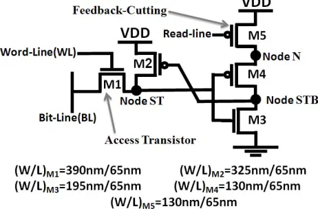
Fig. 2 shows a circuit equivalent to a developed 5T SRAM cell using a supply voltage of 1V in 65-nm technology node. During idle mode of cell (when read and write operation don’t perform on cell) the feedback-cutting transistor (M5) is ON and N node pulled to VDD by this transistor. When '1' stored in cell, M3 and M2 are ON and there is positive feedback between ST node and STB node, therefore ST node pulled to VDD by M2 and STB node pulled to GND by M3. When '0' stored in cell M4 is ON and since N node maintained at VDD by M5 the
STB pulled to VDD, also M2 and M3 are OFF and for data retention without refresh cycle following condition must be satisfied.
3 4
2
1 SD M gate M gate M M
DS I I I
I − > − + − + −
For satisfying above condition when '0' stored in cell, we use leakage current of access transistors (M1), especially sub-threshold current of access transistors (M1).
Fig. 2. New 5T SRAM cell in 65-nm technology node
For this purpose during idle mode of cell, bit-line maintained at GND and word-line maintained at VIdle. Fig. 3 shows leakage current of cell during idle mode for data retention when ‘0’ stored in cell. Most of leakage current of access transistor (M1) is sub-threshold current, since this transistor maintained in sub-threshold region. HSPICE simulation result with VDD=1V shows if during idle mode of cell, bit-line maintained at GND and VIdle =0.2V then ‘0’data stored in cell without refresh cycle and thus in idle mode above condition satisfied. The HSPICE parameters are obtained from the latest Predictive Technology Models (PTMs) for the technology node of 65-nm [6].
A. Read and write operation
During write operation feedback-cutting transistor is ON and N node pulled to VDD by this transistor, thus in write operation read-line maintained at GND. When a write operation is issued the memory cell will go through the following steps.
1)-Bit-line driving: For a write, data drove on bit-line (BL), and then word-line (WL) asserted to VDD.
2)-Cell flipping: this step includes two states as follows:
a)-Data is zero: in this state, ST node pulled down to GND by NMOS access transistor (M1), and therefore the Load transistor (M4) will be ON, and STB node will be pulled up to VDD.
3)-Idle mode: At the end of write operation, cell will go to idle mode and word-line and bit-line asserted to VIdle and GND, respectively.
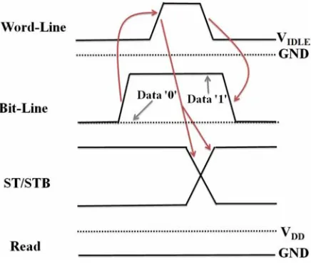
Fig. 4 shows waveform of new cell during write cycles. When a read operation is issued the memory cell will go through the following steps.
1)-Bit-line discharging: For a read, bit-line discharged to GND, and then floated.
Fig. 3. Leakage current in idle mode when ‘0’ stored in cell.
Fig. 4. Waveform of new cell during write cycle.
2)-feedback-cutting: In this step feedback-cutting transistor is OFF and thus read-line maintained at VDD during read operation.
3)-Word-line activation: in this step word-line asserted to VDD, and two states can be considered:
a)-Voltage of ST node is high: when voltage of ST node is high, the voltage of bit-line pulled up to high voltage by NMOS access transistor. We refer to this voltage of bit-line as VBL-High.
b)-Voltage of ST node is low: when voltage of ST node is low, the voltage of bit-line and ST node equalized.
4)-Sensing: After word-line deactivate to VIdle and read-line return to GND then sense amplifier is turned on to read data on bit-line. Fig. 5 shows possible circuit schematic of sense amplifier that used for reading data from new cell.
5)-Idle mode: At the end of read operation, cell will go to idle mode and bit-line asserted to GND, respectively. Fig. 6 shows waveform of new cell during read cycles.
Fig. 5. Possible circuit schematic of sense amplifier.
Fig. 6. Waveform of new cell during read cycle.
B. Cell area
Fig. 7 compares layout of 6T SRAM cell and 5T SRAM cell in scalable CMOS design rules. The 6T SRAM cell has the conventional layout topology and is as compact as possible. The 6T SRAM cell requires 416 λ2 area, whereas 5T SRAM cell requires 345 λ2 area. These numbers do not take into account the potential area reduction obtained by sharing with neighboring cells. Therefore the new cell size is 17% smaller than a conventional six-transistor cell using same design rules.
C. Leakage current
supply voltage to ground and power dissipated. Fig. 8 shows this path when '1' stored in cell.
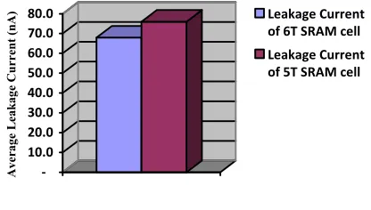
In ordinary programs most of the bits in caches are zeroes for both the data and instruction streams. It has been shown that this behavior persists for a variety of programs under different assumptions about cache sizes, organization and instruction set architectures [7] [8]. Also in [8] from the execution traces of the SPEC2000 benchmarks on average, almost 75% and 64% of bit values are zero in the data and instruction caches, respectively. Thus most of bit values resident in the data and instruction caches are zero. Based on these observations we simulated average leakage current in idle mode of 5T SRAM cell and conventional 6T SRAM cell by using 65-nm PTM. Fig. 9 compares simulated average leakage current of 5T SRAM cell and conventional 6T SRAM cell by using 65-nm PTM, as shown in Fig. 9 the average leakage current of new cell 10% is grater than conventional 6T SRAM cell. It is quite clear, the cache based on new cell contains other component except cell array, and thus the effect of leakage current of cells on total leakage current of cache is less than 10%.
Fig. 7. Layout comparison of 5T cell and 6T cell.
Fig. 8. Path from supply voltage to ground when '1' stored in cell.
IV. DYNAMIC ENERGY CONSUMPTION
In a cache, the major dynamic energy consuming components are bit-lines, word-lines, sense amplifiers,
decoders and output drivers [1]. In general, the bit-lines are the most power consuming component [1]. Therefore energy consumption during cache access consumed due to the transitions occur during read/write operation, and thus during each cache access a certain amount of energy is drawn from the power supply and dissipated. The energy consumption of each cache access depends on type of cache access (read or write).
When the capacitor CL charged by a transistor from GND to VDD and then discharged to GND by another transistor or same transistor, amount of energy is drawn from the power supply and dissipated, equals CLVDD2 [9]. The stored energy on the capacitor CL with voltage VC
equals CLVC2 2 1
. Thus each time the capacitor CL charged
from VC to VDD by a transistor and then discharged to VC by another transistor, amount of energy drawn from the power supply and dissipated, obtained by following expression.
) ( DD2 C2
L
Supply C V V
E = −
(1) In following dynamic energy consumption in each cache access of 5T and 6T SRAM cell investigated analytically, and since sense amplifiers, decoders and output drivers in cache based on 5T cell and 6T cell approximately have same dynamic energy consumption and dynamic energy consumption of decoders and output drivers didn’t depend on type of cell (5T or 6T) we ignore the dynamic energy consumption due to sense amplifiers, decoders and output drivers. Also symbols and parameters that we use throughout our analytical modeling are listed in Table 1.
‐ 10.0 20.0 30.0 40.0 50.0 60.0 70.0
80.0 Leakage Current
of 6T SRAM cell Leakage Current of 5T SRAM cell
Fig. 9. Average leakage current comparison of 5T SRAM cell and 6T SRAM cell with the 65-nm PTM.
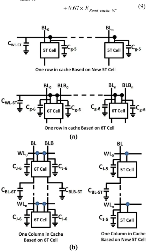
A. Capacitance in 5T SRAM cell and 6T SRAM cell Fig. 10 shows a column and a row of cache based on novel 5T cell and basic 6T cell. According to this figure we can write following expression.
T BL ct Interconne T
Access Junction T
BL C C
C −5 = − −5 + − −5
(2)
T WL ct Interconne T
Access Gate T
WL C C
C −5 = − −5 + − −5
(3)
ad ct Interconne Cutting
Feedback Gate T
ad C C
CRe −5 = − − + −Re
(4)
Aver
age L
eak
age
Current (n
T BL ct Interconne T Access Jounction T BLB T BL C C C C 6 6 6 6 − − − − − − + = = (5) T WL ct Interconne T Access Gate T
WL C C
C −6 = − −6 + − −6
(6)
B. Dynamic energy consumption of conventional 6T SRAM cell
When a write operation is issued, a cache based on 6T SRAM cell will go through the following steps:
1)-Bit-line driving: For a write operation, this bit-line driving performed by turning on proper write buffer. After this step, the bit-line pair will be forced into full-swing logic level and then word-line asserted to VDD [10].
2)-Cell flipping: If the value of the stored bit in the cell is the opposite to the value being written, then the cell flipping process will take place [10].
3)-Pre-charging: At the end of the write operation, word-line pulled to GND and bit-word-line pair pre-charged to VDD [10].
Thus based on above writing process, when a write operation performed on a cache with 6T SRAM cell following transitions occur on word-line and bit-lines.
1-Word-line charged from GND to VDD and then discharged to GND. Consequently amount of energy drawn from power supply and dissipated isCWL-6TVDD2.
2-BL or BLB from VDD discharged to GND and then charged to VDD. Consequently amount of energy drawn from power supply and dissipated isCBL-6TVDD2.
Therefore, when caches based on 6T SRAM cell accesses with write operation amount of energy is drawn from power supply and dissipated approximately obtained by following analytical expression.
2 DD 6T -BL 2 DD 6T -WL 6T -cache
-Write C V C V
E = +
(7) When a read operation is issued a cache based on 6T SRAM cell will go through the following steps:
1)-Word-line activation: At this step word-line asserted to VDD and access transistors connect cell to their bit-lines [10].
2) - Bit-line deriving: After word-line asserted to high voltage, the target cell connected to their bit-lines. The so-called cell current through a drive transistor of target cell will discharge voltage of BL or BLB to VBL-Low [10].
3)-In this step sense amplifier is enabled to read data on bit-lines [10].
4)-At the end of read operation word-line return to GND and bit-line pair per-charged to VDD [10].
Thus based on above reading process, when a read operation performed on cache with 6T SRAM cell following transitions occur on word-line and bit-lines:
1-Word-line charged from GND to VDD and then discharged to GND. Consequently amount of energy drawn from power supply and dissipated isCWL-6TVDD2.
2-BL or BLB from VDD discharged to VBL-LOW and then charged to VDD. Consequently amount of energy drawn
from power supply and dissipated is )
( 2 2
6T DD BL LOW
BL V V
C − − − .
Therefore, when a read operation performed on a cache based on 6T SRAM cell amount of energy is drawn from power supply and dissipated approximately obtained by following analytical expression.
)
( 2 2
6T DD BL Low BL 2 DD -6T WL -6T cache -Read V V C V C E − − − + = (8)
In the instruction cache, because all accesses are cache reads, cache writes only occur in case of misses. In the data cache, the cache writes also arise in the execution of STORE instruction besides the cache misses [1]. The proportion of cache writes to reads is about 1: 2 in data cache [11]. Thus based on these observations in worst case 33% of accesses are write and 67% are read and the average dynamic energy consumption in a cache access can be estimated by following expression.
6T -cache -Read 6T -cache -Write 6T -cache -Access E 0 E E × + × = 67 . 33 . 0 (9) (a) (b)
C. Dynamic energy consumption of novel 4T-SRAM cell
Based on read and write operation described in Section 3, when write operation is issued depending on the value must be stored in the cell, there are two cases in write energy consumption: one is write '0' and the other is write '1'.
a)-In the case of write '0' following transitions occur on word-line.
1-Word-line charged by a transistor from VIdle to VDD and then discharged to VIdle. Consequently amount of energy drawn from power supply and dissipated isCWL-5T(VDD2 −VIdle2).
Thus in this case the energy consumption estimated by following expression. ) 2 Idle 2 DD 5T -WL 5T -cache -0
-Write C (V V
E = −
(10)
b)-In the case of write '1' following transitions occur on word-line and bit-line.
1-Word-line charged by a transistor from VIdle to VDD and then discharged to VIdle. Consequently amount of energy drawn from power supply and dissipated isCWL-5T(VDD2 −VIdle2).
2-BL charged by a transistor form GND to VDD and then discharged to GND. Consequently amount of energy drawn from power supply and dissipated isCBL-5TVDD2. Thus in this case the energy consumption estimated by following expression. 2 DD 5T -BL Idle 2 DD 5T -WL 5T -cache --1 Write V C V (V C E + −
= 2)
(11)
In [1] from the execution traces of the SPEC2000 benchmarks around 85% of the instruction write bits are '0' and over 90% of the data write bits are '0'. Therefore, in worst case when a write operation performed on cache with novel 5T SRAM cell on average amount of energy is drawn from power supply and dissipated approximately obtained by following analytical expression.
T cache Write T cache Write 5T -cache -Write E E E 5 1 5 0 15 . 0 85 . 0 − − − − − − × + × = (12) When the read operation is issued depending on the value stored in the cell, there are two cases in read energy consumption: one is read '0' and the other is read '1'.
a)-In the case of read '0' following transition occur on word-line and read-line.
1- Word-line charged by a transistor from VIdle to VDD and then discharged to VIdle. Consequently amount of energy drawn from power supply and dissipated isCWL-5T(VDD2 −VIdle2).
2- Read-line charged by a transistor from GND to VDD and then discharged to GND. Consequently amount of energy drawn from power supply and dissipated isCRead-5TVDD2.
Thus in this case the energy consumption estimated by following expression. 2 DD 5T -Read Idle 2 DD 5T -WL V C V (V C + − = )
ERead-0-cache-5T 2
(13)
b)-In the case of read '1' following transitions occur on word-line1 and BLB.
TABLE I.
SUMMARY OF NOTATIONS USED IN THE ANALYTICAL MODEL.
Symbol Parameter
Cg-6T,Cg-5T Gate capacitance of access transistor 6T and 5T SRAM cell
CJ-6T,CJ-5T junction capacitance of access transistor 6T and 5T SRAM cell
CJunction-Access-5T, CJunction-Access-6T
Load capacitance due to junction capacitance of access transistors connected
to bit-line CInterconnect-BL-5T,
CInterconnect-BL-6T
Load capacitance due metal of bit-line
CGate-Access-5T, CGate-Access-6T
Load capacitance due to gate capacitance of access transistors connected to word-line
CInterconnect-WL-5T, CInterconnect-WL-6T
Load capacitance due metal or poly of word-line
CGate-Feedback-Cutting Load capacitance due to gate capacitance of feedback-cutting transistors connected to
read-line
CInterconnect-Read Load capacitance due metal or poly of read-line
CBL-6T,CBL-5T BL capacitance of a cache based on 6T and 5T SRAM cell
CRead-5T Read-line capacitance of a cache based on 5T SRAM cell
CWL-5T, CWL-6T Word-line capacitance of a cache based on 5T and 6T SRAM cell CBLB-6T BLB capacitance of a cache based on 6T
SRAM Cell
VDD Supply voltage
VBL-Low Voltage of BL or BLB during read operation in a cache based on 6T Cell VBL-High Voltage of BL during read operation in a
cache based on 5T SRAM Cell VIdle Voltage of word-line during idle mode in
5T SRAM Cell
EWrite-Cache-6T Average Energy consumption of write operation in cache based on 6T SRAM Cell ERead-Cache-6T Average Energy consumption of read
operation in cache based on 6T SRAM Cell EAccess-Cache-6T Average Energy consumption during cache access in cache based on 6T SRAM Cell EWrite-0-Cache-5T Energy consumption of writing zeros in
cache based on 5T SRAM Cell EWrite-1-Cache-5T Energy consumption of writing ones in
cache based on 5T SRAM Cell ERead-0-Cache-5T Energy consumption of reading zeros in
cache based on 5T SRAM Cell EWrite-1-Cache-5T Energy consumption of reading ones in
cache based on 5T SRAM Cell EWrite-Cache-5T Average Energy consumption of write
operation in cache based on 5T SRAM Cell ERead-Cache-5T Average Energy consumption of read
1- Word-line charged by a transistor from VIdle to VDD and then discharged to VIdle. Consequently amount of energy drawn from power supply and dissipated isCWL-5T(VDD2 −VIdle2).
2- Read-line charged by a transistor from GND to VDD and then discharged to GND. Consequently amount of energy drawn from power supply and dissipated isCRead-5TVDD2.
3-BL charged by a transistor form GND to VBL-High and then discharged to GND. Consequently amount of energy drawn from power supply and dissipated isCBL-5TVBL-High2.
Thus in this case the energy consumption estimated by following expression. 2 DD 5T -Read 2 DD 5T -Read Idle 2 DD 5T -WL T cache ad V C V C V (V C E + − − − + −
= 2)
5 1 Re
(14)
Over 70% of the bits that are read from the cache are zeros [3]. Therefore, when a read operation performed on cache with novel 4T SRAM cell on average amount of energy is drawn from power supply and dissipated approximately obtained by following analytical expression. T cache ad T cache ad 5T -cache -Read E E E 5 1 Re 5 0 Re 3 . 0 7 . 0 − − − − − − × + × = (15) As mentioned above, around 33% of accesses are writing and 67% are reading. Thus in cache with new 5T cell, we can estimate worst case average dynamic energy consumption of cache access by following expression.
5T -cache -Read 5T -cache -Write 5T -cache -Access E 0 E E × + × = 67 . 33 . 0 (16)
D. Dynamic energy consumption Comparison
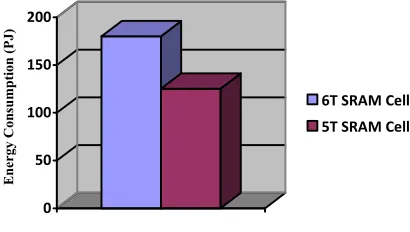
Fig. 11 shows the average dynamic energy consumption in a cache access of novel SRAM cell and 6T SRAM cell by using parameter values listed in Table 2. As shown in Fig. 11 the average dynamic energy consumption in cache accesses of cache based on novel SRAM cell is %30 smaller than cache based on 6T SRAM cell. For this reduction there are two obvious reasons as follows. First, in writing and reading zero of new cell there is not any change on bit-line since bit-line maintained at GND in idle mode. Therefore the energy consumption of writing and reading zero are smaller than writing and reading one. Second, reading '0' or writing '0' occurs more frequently than reading '1' or writing '1'.
V. EXPERIMENTAL RESULTS
To verify correct operation of new 5T SRAM cell and comparison with 6T SRAM cell, we simulate a 5T SRAM cell and 6T SRAM cell using HSPICE with 1V for supply voltage also the HSPICE parameters are obtained from the latest Predictive Technology Models
(PTMs) for the technology node of 65-nm [6]. Based on layouts shown in Fig. 7, and with using Tanner L-Edit CAD tool we extract the HSPICE Netlist of novel 5T SRAM cell and 6T SRAM cell. Also based on layouts shown in Fig. 7, all parasitic capacitances and resistances of bit-lines, word-lines are included in the circuit simulation. For testing the correctness of a read and write operation of new 5T SRAM cell, following scenario applied to new 5T SRAM cell:
a)-Writing ‘0’ in to new cell and then read it. b)-Writing ‘1’ in to new cell and then read it.
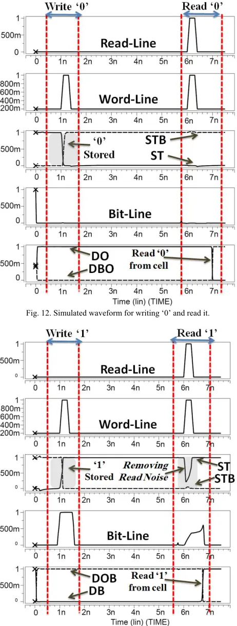
Fig. 12 and Fig. 13 show simulated waveform with applying above scenario. As shown in Fig. 12 when '0' read from new 5T cell there is not any read noise on ST node but as shown in Fig. 13 when '1' read from new 5T cell, ST node pulled to low voltage, because Bit-line floated at GND during read operation. Since during read operation feedback-cutting transistor is OFF, consequently there is not any relation between ST node and STB node and finally injected noise by access transistor during reading '1' removed by core of cell. Based on simulation results and analytical results of previous sections, Table 3 compares the novel 5T SRAM cell and Basic 6T SRAM cell. The average cache access delay is defined as the average elapsed time for performing read or writes operation without including write buffer delay and sense amplifier delay. Also the static noise margin (SNM) is defined as the maximum value of DC disturbances that can be tolerated before the cell’s storage value is flipped [12].
As shown in Table 3 the new 5T cell is 20% faster than 6T cell. For this speed improvement there are two obvious reasons as follows. First, in new 5T cell there is not any relation between read SNM and cell current. Thus we can increase the cell current of new cell without any read SNM degradation. Whereas in 6T cell any increasing the cell current for speed improvement resulting read data destruction. Second, W/L of access transistor of new cell selected greater than W/L of access transistors of 6T cell for speed improvement. Therefore the cell current of new 5T cell is higher than 6T cell and this resulting faster transition on ST and STB node and bit-line.
0 50 100 150 200
6T SRAM Cell 5T SRAM Cell
Fig. 11. Average dynamic energy consumption of a cache with 5T SRAM cell and with 6T SRAM cell.
Fig. 12. Simulated waveform for writing ‘0’ and read it.
Fig. 13. Simulated waveform for writing ‘1’ and read it.
VI. CONCLUSION
With the aim of achieving a high density and low power cache, we developed a 5T SRAM cell. The key observations behind our design are that dynamic occurrence of zeros in the cache access stream and
cache-resident memory values of ordinary programs exhibit a strong bias towards zero. New cell retains its data with leakage current when there is not any positive feedback. In same design rules proposed cell area is 17% smaller than 6T SRAM cell with 20% speed improvement. Dynamic energy consumption during cache access of new cell is 30% smaller than 6T SRAM cell but the proposed cell is with 10% cell leakage current penalty.
TABLE II.
PARAMETER VALUES USED IN ANALYTICAL EXPRESSIONS.
Symbol Value
CWL-6T 0.8pF
CWL-5T 0.9pF
CBL-6T, CBLB-6T 1.35pF
CBL-4T 1.5pF
VDD 1V
VIdle 0.3V
VBL-Low 0.7V
VBL-High 0.5V
TABLE III.
PERFORMANCE COMPARISONS OF SRAM CELLS
Metrics 6T SRAM Cell 5T SRAM Cell
Average Cache Access Delay
180ps 143ps
Static Noise Margin 0.45V 0.5V
Average Leakage Current 68nA 76nA
Average Dynamic Energy Consumption in Cache
Access
180pJ 125pJ
Read Static Noise Margin 0.3V Free
REFERENCES
[1] Y. J. Chang, F. Lai, and C. L. Yang, “Zero-Aware Asymmetric SRAM Cell for Reducing Cache Power in Writing Zero,” IEEE Transactions on Very Large Scale Integration Systems, vol. 12, no. 8, pp. 827-836, 2004. [2] A. Kotabe, K. Osada, N. Kitai, M. Fujioka, S. Kamohara,
M. Moniwa, S. Morita, and Y. Saitoh, “A Low-Power Four-Transistor SRAM Cell With a Stacked Vertical
Poly-Silicon PMOS and a Dual-Word-Voltage Scheme,” IEEE
Journal of Solid-State Circuits, vol. 40, no. 4, pp. 870-876, 2005.
[3] L. Villa, M. Zhang, and K. Asanovic, “Dynamic zero
compression for cache energy reduction,” in Proceeding 33rd Annual IEEE/ACM International Symposium Microarchitecture, pp. 214–220, 2000.
[4] K. Takeda et al., “A read-static-noise-margin-free SRAM cell for low-VDD and high-speed applications,” IEEE Journal of Solid-State Circuits, vol. 41, no. 1, pp. 113-121, 2006.
[6] http://www.eas.asu.edu/~ptm & W. Zhao and Y. Cao, “New generation of predictive technology model for sub-45nm design exploration,” IEEE Transactions on Electron Devices, vol. 53, no. 11, pp. 2816-2823, 2006.
[7] N. Azizi, F. Najm, and A. Moshovos, “Low-leakage
asymmetric-cell SRAM,” IEEE Transactions on Very
Large Scale Integration Systems, vol. 11, no. 4, pp. 701– 715, 2003.
[8] A. Moshovos, B. Falsafi, F. N. Najm, and N. Azizi, “A
Case for Asymmetric-Cell Cache Memories,” IEEE
Transactions on Very Large Scale Integration Systems, vol. 13, no. 7, pp. 877-881, 2005.
[9] J. M. Rabaey, A. Chandrakasan, and B. Nikolic, Digital Integrated Circuits: A Design Perspective, Prentice Hall, 2002.
[10]K. Martin, Digital Integrated Circuit Design, Oxford University Press, New York, 2000.
[11]J. L. Hennessy and D. A. Patterson, Computer
Architecture: A Quantitative Approach, San Mateo, Morgan Kaufmann, 1995.
[12]E. Seevinck, F. J. List, and J. Lohstroh, “Static-noise
margin analysis of MOS SRAM cells,” IEEE Journal of
Solid-State Circuits, vol. SC-22, no. 5, pp. 748–754, 1987.
Arash Azizi Mazreah received the B.S. degree in computer hardware engineering and M.S. degree in computer system architecture engineering in 2005 and 2007 respectively. Currently he is a Ph.D. candidate in computer system architecture engineering at Islamic Azad University, Science and Research Branch and faculty of Islamic Azad University, Sirjan branch. His major research experiences and interests include low power digital system design, high speed SRAM, and VLSI testing and high density VLSI system design.
Mohammad Taghi Manzuri received his B.S. and M.S. in Electrical Engineering from Sharif University of Technology, Iran, in 1984 and 1988, respectively; and Ph.D. in Electrical and Computer Engineering from Vienna University of Technology, Austria, in 1995. Currently, he is an associate professor in Computer Engineering Department of Sharif University of Technology, Tehran, Iran. His main research interests include digital signal processing, robotics, image processing, and data communications.