Impact Factor: 2.745 (SIJF)
Int. J. of Engg. Sci. & Mgmt. (IJESM), Vol. 4, Issue 4: Oct. – Dec.: 2014, 33-39
INTERNATIONAL JOURNAL OF ENGINEERING SCIENCES &
MANAGEMENT
AN EFFICIENT DESIGN OF 1 BIT ARITHMETIC LOGIC UNIT IN QUANTUM DOT
CELLULAR AUTOMATA
Sandeep Patidar
*, Mukesh Tiwari
1*,1
Department of Electronics, SSSIST, Sehore (MP)
ABSTRACT
Quantum cellular automata (QCA) is an attractive emerging technology that takes advantage of quantum effects,
which become increasingly apparent at the scale of a few nanometers. Previous work has shown that QCA has
several novel features not available with conventional FET-based circuits. We describe the design of 1-bit
Arithmetic Logic Unit based on combinational circuits which reduces the required hard-ware complexity and
allows for reasonable simulation times. Our aim is to provide evidence that QCA has potential applications in
future computers provided that the underlying technology is made feasible. The 1-bit Arithmetic logic unit (ALU)
consist arithmetic unit, logical unit and full adder are major blocks of ALU. The design of ALU is successfully
implemented using QCADesigner tool and also verified the simulation result of 1-bit ALU.
Keywords- Arithmetic Logic Unit, Nanotechnology, QCA
INTRODUCTION
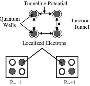
Quantum Cellular Automata (QCA) refers to quantum computation, which have been devised in analogy conventional models of cellular automata introduced by von Neumann. The QCA also refer to quantum dot cellular automata, which proposed the physical implementation of “classical” cellular automata exploiting quantum mechanical phenomena. Quantum Cellular Automata has attracted a lot of attention as a result of its extremely small feature size (at the molecular or even atomic scale) and its ultra low power consumption, making it one candidate for replacing CMOS technology. In QCA, a quantum cell normally consists of four quantum dots at corner of a square, with two excess electrons that are free to tunnel between the dots but which cannot leave the cell. As per coulomb repulsion, these two electrons tend to occupy diagonally opposite dots. In a second type of QCA cell, the dots are located at the middle of the side of the cell, instead of the corners. In either cell type, there are just two configurations with energetically equivalent polarization designated as +1 and -1. This means that quantum cells can be employed as binary system to represent logical true and false (or digital 1 and 0). Moreover, multiple quantum cells can be arranged in various linear formations to produce logic gates, which can in turn be used to build devises foe computation. The basic logic elements in QCA logic are the majority gate and the inverter (or NOT gate). An arithmetic and logic unit (ALU) is a digital circuit that performs the arithmetic and logical operations. The ALU is a basic building block of the central processing unit of a computer, and the microprocessors contain one for maintaining timers. The processor found inside the CPUs and graphics processing units (GPUs) suit very powerful and very complex LAUs; a single component may contain a number of ALUs. The ALU concept proposes by Mathematician John von Neumann in 1945. He wrote a report on foundation for a new computer called the EDVAC. Research into ALUs remains an important part of computer science, falling under arithmetic and logic structure in the ACM Computing Classification System
QCA REVIEW A. Background
Int. J. of Engg. Sci. & Mgmt. (IJESM), Vol. 4, Issue 4: Oct. – Dec.: 2014, 33-39
Figure No. 1(a): QCA cell and its PolarizationQCA wire is formed by an array of QCA cells shown in Figure No. 1(b), which provides a medium for data propagation based on Coulomb interactions.
Figure No. 1(b): QCA Wire
Figure No. 1(c): QCA inverter
Figure No. 1(d): QCA Majority Voter
The polarization of the output QCA cell ‘out’ or ‘output’ is the opposite of the polarization of input QCA cell ‘in’ or ‘input’. QCA majority voter (MV) and its logic symbol are shown in Figure No. 3(a), MV, is equivalent to a logic function F(A,B,C)=AB+AC+BC and can be implemented by five QCA cells arranged in a cross. Cells A, B, and C are input cells, and cell D is the output cell that is polarized according to the polarization of the majority of the input cells. For example, since two (out of three) input QCA cells are polarized to -1. The output cell is also polarized to be -1 (see Figure No. 3(b)). Logical AND and OR functions can be implemented from majority voter by presetting one input immutably to binary values 0 and 1, respectively [1-5],[8].
B. QCA Clocking
A QCA cell has four clock phases; they are Switch, Hold, Release and Relax [6, 7]. Figure No. 2 shows four phases of the QCA clock operation process. During the switch phase, QCA cells begin un-polarized and their inter dots potential barriers are low. The barriers are then raised during this phase, and the QCA cells become polarized according to the state of their driver (i.e. their input cell). It is in this clock phase that the actual computation (or switching) occurs. By the end of this clock phase, barriers are high enough to suppress any electron tunneling and cell states are fixed. During the hold phase, barriers are held high so the outputs of the sub array can be used as inputs to the next stage. In the release phase, barriers are lowered and cells are allowed to relax to an un-polarized state. Finally, during the fourth clock phase, the relax phase, cell barriers remain lowered and cells remain in an
Quantum Wells
Tunneling Potential
Junction Tunnel
P= -1 P=+1
Binary 0
Binary 1
Localized Electrons
1 0
A
Input Output
0
0
0 1
Input A
Input B
Input C
Output D
Impact Factor: 2.745 (SIJF)
Int. J. of Engg. Sci. & Mgmt. (IJESM), Vol. 4, Issue 4: Oct. – Dec.: 2014, 33-39
un-polarized state [6, 7]. In the meantime, the large scale QCA circuit is partitioned into four clock zones; Figure No. 2 shows each clock zone signal and demonstrates the pipeline mechanism. All cells in a certain zone are controlled by the same QCA clock signal. Cells in each zone perform a specific calculation; the state of a zone is then fixed so that it can serve as input signals to the next zone. Information transfers in a pipelined fashion.
Figure No. 2: Clocking Zones C. Three-bit AND & OR using Majority Voter Gate
Figure No. 3 (a) 3-bit AND Figure No. 3 (b) 3-bit OR
ARCHITECTURE OF ARITHMETIC LOGIC UNIT
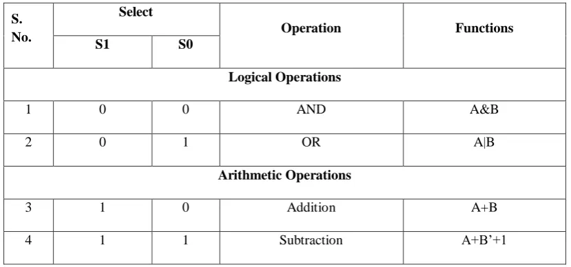
An Arithmetic Logic Unit (ALU) is a multi-operation, combinational-logic digital function. It can perform a set of basic arithmetic operations and a set of logic operation. The ALU has a number of selection lines to select a particular operation in the unit. The Arithmetic Logic Unit consists three basic units; arithmetic unit, logical unit and full adder circuit. In addition to these operations it also takes AND of two numbers and OR of two numbers. M and S are the select signals that decide which operation are performed. M is a select line to select operations either arithmetic or logical. The function table for the four operations performed by the ALU is shown in Table No. 1.
S. No.
Select
Operation Functions
S1 S0
Logical Operations
1 0 0 AND A&B
2 0 1 OR A|B
Arithmetic Operations
3 1 0 Addition A+B
4 1 1 Subtraction A+B’+1
Table No. 1: Function Table of Arithmetic Logic Unit
A. Arithmetic Unit
Clock Zone 0
Clock Zone 1
Clock Zone 2
Clock Zone 3
Input
Input
Input
P= -1
Output Cell Output Cell
Input
Input
Input
Int. J. of Engg. Sci. & Mgmt. (IJESM), Vol. 4, Issue 4: Oct. – Dec.: 2014, 33-39
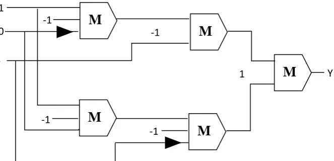
The Arithmetic Unit modifies the second operand and passes it to the Full Adder to perform the arithmetic. Arithmetic is the oldest and most elementary branch of mathematics, used by almost everyone, for tasks ranging from simple day-to-day counting to advanced science and business calculations. It involves the study of quantity, especially as the result of operations that combine numbers.
S1 S0 A B Y
1 0 0 0 0
1 0 0 1 1
1 0 1 0 0
1 0 1 1 1
1 1 0 0 1
1 1 0 1 0
1 1 1 0 1
1 1 1 1 0
Table No. 2: Truth table of Arithmetic Unit
Figure No. 4: Schematic diagram of Arithmetic Unit B. Logical Unit
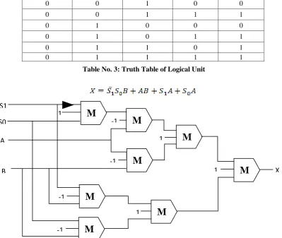
The logic operations are performed in the logic Unit. The Full adders are used simply as connections for the outputs. In logic and mathematics, a two-place logical operator and, also known as logical conjunction, results in trueif both of its operands are true, otherwise the value of false.
M
M
M
M
M
S1
S0
B
1 -1
-1
-1
-1
Impact Factor: 2.745 (SIJF)
Int. J. of Engg. Sci. & Mgmt. (IJESM), Vol. 4, Issue 4: Oct. – Dec.: 2014, 33-39
S1 S0 A B X
0 0 0 0 0
0 0 0 1 0
0 0 1 0 0
0 0 1 1 1
0 1 0 0 0
0 1 0 1 1
0 1 1 0 1
0 1 1 1 1
Table No. 3: Truth Table of Logical Unit
Figure No. 5: Simplified schematic diagram of logical Unit IMPLEMENTATION OF 1 BIT ALU IN QCA
Implementation of one bit ALU in QCA is verified using QCA Designer tool. The proposed design is shown in Figure No. 6.
Figure No. 6: Implementation of 1 bit ALU in QCA
B
M
M
M
M
M
M
M
M
1
1
1
1 -1
-1
-1 -1
A S0
S1
Int. J. of Engg. Sci. & Mgmt. (IJESM), Vol. 4, Issue 4: Oct. – Dec.: 2014, 33-39
SIMULATION RESULTS AND DISCUSSIONAll the designs were verified using QCADesigner tool ver. 2.0.3. In the bi-stable approximation, we used the following parameters: cell size=18 nm, number of samples=12800, convergence tolerance=0.001000, radius of effect=65.00 nm, relative permittivity=12.900000, clock high=9.800000e-022, clock low=3.800000e-023, clock amplitude factor=2.000000, layer separation=11.500000, maximum iteration per sample=100. All of these parameters which used are default parameters in QCADesigner tool. In our QCA layouts, we have the goal of workable designs with compact layout. The simulation Results of one bit ALU is shown in Figure No. 7.
Figure No. 7: Simulation result of 1 bit ALU CONCLUSION
This paper proposes one bit ALU (Arithmetic Logic Unit) in QCA which uses arithmetic and Logical Extender and Full adder. The proposed work shows that the Functions of ALU design in QCA is same as traditional ALU designed in CMOS technology. By using QCA we have reduces complexity, size, power consumption, delay & cost and Improve the performance of ALU is much beneficial.
In future, we will design 2-bit, 4-bit & 8-bit ALU in QCA. We will also design 1-bit ALU (Arithmetic Logic Unit) using Reversible logic gates in QCA.
REFERENCES
[1] M.G. Waje, P.K. Dakhole, “Design and Implementation of 4-bit Arithmetic Logic Unit using Quantum Dot Cellular Automata”, 2013 3rd IEEE International Advance Computing Conference (IACC), pp. 1012-1017 [2] S. Karthigai Lakshmi, G. Athisha, “Design and Analysis of Subtractors using Nanotechnology Based QCA”
European Journal of Scientific Research, vol. 53, No. 4, 2011, pp 524-32.
[3] P.D. Tougaw and C. S. Lent, “Logical devices implemented using quantum cellular automata,” J. Appl. Phys., American Institute ofPhysics, vol. 75, pp.1818-1824, 1994.
[4] A. Vetteth, K. Walus, V. S. Dimitrov, and G. A. Jullien,"Quatum-dotcellular automata carry-look-ahead adder and barrelshifter,”in Proc. IEEE Emerging Telecommunications Technologies Conference, Dallas, TX, Sept. 2002.
[5] KrishnaveniD., GeethaPriya.M, “A Novel Design of Reversible Serial and Parallel Adder/Subtractor” International Journal of Engineering Science and Technology (IJEST), vol. 3, No.3,March 2011, pp 2280-88. [6] H. Thapliyal and N. Ranganathan, "Conservative QCA Gate (CQCA) for Designing Concurrently Testable
Impact Factor: 2.745 (SIJF)
Int. J. of Engg. Sci. & Mgmt. (IJESM), Vol. 4, Issue 4: Oct. – Dec.: 2014, 33-39
[7] R. Landauer, "Irreversibility and Heat Generation in the Computational Process," IBM Journal of Research and Development, vol. 5, 1961.
[8] C. Bennett, "Logical Reversibility of Computation," IBM Journal ôf Research and Development, vol. 17, 1973, pp 525-532.
[9] Kerntopf, P; Khan, M.H.A.; Perkowski, M.A, 2004. On universality of general reversible multiple value Logic gates, IEEE proceeding of the 34th international symposium on multiple valued logic (ISMVL’04), pp: 68‐73.
[10]Kerntopf, P; Perkowski, M, 2001.Reversible Logic. Invited tutorial, Proc.EURO‐MICRO, Sept 2001, Warsaw, Poland.
[11]K. Hennessy and C. S. Lent, "Clocking of molecular quantum-dot cellular automata," Journal of Vacuum Science & Technology vol. 19, no. 5, pp.1752 1755, 2001
[12]J. Smolin and D. Divincenzo, "Five Two-bit Quantum Gates Are Sufficient to Implement the Quantum A, vol. 53, 1996, pp 2855-6 Fredkin Gate," Physical Review
[13]Krishnaveni,D, Geetha Priya,M, “Design of an Efficient Reversible 8x8 Wallace Tree Multiplier”, Submitted for Review to Circuits and Systems-I Journal, IEEE.