http://www.sciencepublishinggroup.com/j/ajmp doi: 10.11648/j.ajmp.20180704.14
ISSN: 2326-8867 (Print); ISSN: 2326-8891 (Online)
Modeling and Characterization of Inconsistent Behavior of
Gate Leakage Current with Threshold Voltage for Nano
MOSFETs
Yashu Swami
*, Sanjeev Rai
Department of Electronics & Communication Engineering, Motilal Nehru National Institute of Technology Allahabad, Allahabad, India
Email address:
*
Corresponding author
To cite this article:
Yashu Swami, Sanjeev Rai. Modeling and Characterization of Inconsistent Behavior of Gate Leakage Current with Threshold Voltage for Nano MOSFETs. American Journal of Modern Physics. Vol. 7, No. 4, 2018, pp. 166-172. doi: 10.11648/j.ajmp.20180704.14
Received: July 13, 2018; Accepted: August 19, 2018; Published: September 15, 2018
Abstract:
A strange relationship of gate leakage current and threshold voltage variation for nano MOSFETs is analyzed using factual strategy and subsequently a physical model is proffered. The gate leakage current increments with the threshold voltage before it diminishes at higher threshold voltage in nanoscale devices. This inconsistent behavior of gate leakage current with threshold voltage variations is precisely clarified in the manuscript through the concept of accord between two contrary operations: threshold voltage roll-off impact and gate leakage current reliance on surface potential. The tunneling gate leakage current density diminishes with threshold voltage over surface potential. However, the threshold voltage roll-off impact causes higher threshold voltage for larger channel length devices. The net gate leakage current is adjusted by these two contrary functions of threshold voltage. In addition, the rate of accretion of the gate leakage current with threshold voltage variation is also analyzed. The impact of the increase in the power supply voltage on the rate of accretion of the gate leakage current vs. threshold voltage curve is also explored. Thorough methodical TCAD simulations are accomplished to validate the proffered models. Both the experimental outcomes, TCAD simulations and physics based models are implemented to uncover and clarify the threshold voltage gate leakage relationship, particularly for nano MOSFETs. The proposed notion is not currently captured in conventional gate leakage nano device models, hence the proffered physical models may be utilized in progression of reliable and trustworthy TCAD simulation tools for nano devices.Keywords:
Gate Leakage Current, Line-Edge Roughness, Nano MOSFET, Oxide Thickness Variation, Random Dopant Fluctuation, Threshold Voltage Roll-off Impact1. Introduction
The device characteristic variations have developed as a noteworthy barrier for CMOS technology scaling [1-3]. Of specific significance is the factual variation of threshold voltage (VTH) and gate leakage current (IGL) which confines
the power and performance measurements. It also prompts to critical output restrictions for both analog, digital and computerized memory/SRAM design [4-6]. A physical comprehension of the threshold voltage and gate leakage current (VTH)-(IGL) relationship is critical for both device
modeling and circuit design especially at nanoscale technology [7-10]. It has been noted that the (VTH)-(IGL)
relationship to a great extent has been overlooked and ignored
for long channel devices, profoundly scaled 45nm and past technologies. However, the (VTH)-(IGL) relationship cannot be
ignored for nano devices, particularly for below 45nm scaled technologies. In this manuscript, we present a comprehensive study on characterizing the inconsistent behavior of gate leakage current with threshold voltage variation particularly for nano MOSFETs. The inconsistent (VTH)-(IGL) relationship
is accurately modeled after analyzing the experimental measurements and factual investigation performed on more than 20,000 MOSFETs fabricated with advanced 45nm
based models are acquainted to uncover and clarify the (VTH)-(IGL) relationship particularly for nano MOSFETs.
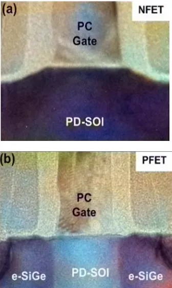
Figure 1. TEM image of a PD-SOI (a) N-MOSFET and (b) P-MOSFET device used to examine and model inconsistent (VTH)-(IGL) relationship.
2. Model Device Fabrication Approach
For the comprehensive study on characterizing the inconsistent behavior of gate leakage current with threshold voltage variation, PD-SOI MOSFETs are fabricated utilizing 45nm technology. Figure. 1 represents the typical cross-section TEM image of a N-MOSFET and P-MOSFET device used to examine and model inconsistent (VTH)-(IGL)
relationship using four discrete threshold voltage device designs (VTH1-VTH4) [7]. The device development highlights
the fabrication process with the following features: numerical aperture value of 1.2, 193nm immersion lithography designing, enhanced Dual-Stress Liner (DSL), Stress Memorization Technique (SMT), Advanced Annealing (AA), and close-proximity embedded advanced e-SiGe [11-12]. The model MOSFETs with Poly-Si/SiON gate stack are fabricated for four discrete threshold voltages (VTH1 - VTH4) with their
nominal threshold voltage characteristics as
VTH1<VTH2<VTH3<VTH4. The threshold voltage variance
features are acknowledged through the substrate and halo doping practice. The device dimension measurements are assessed by adjusting the physical estimations in TEM and XPS. N-MOSFET contains 10 fingers with a width (WF) of
400nm and normal gate length (LG) of 40nm for each finger.
Threshold voltage is characterized by Constant Current Threshold Voltage Extraction Technique (CCM) [13-14] and estimated at VDS=VDD for VTSAT and VDS=50mV for VTLIN. The
VTSAT and VTLIN represent the respective threshold voltages of
the device while operating in saturation and linear region. Gate leakage current (IGL) is estimated under inversion
condition where VGS=VDD. The VDD is biased at 0.9V.
Figure 2. Gate leakage current extracted under inversion condition as for (a) VTSAT and (b) VTLIN for N-MOSFETs with discrete limit voltages (VTH1-VTH4).
For VTH1 to VTH4 device lot, the rate of increment of gate leakage current with
the threshold voltage variations is accordingly represented by Ө1 to Ө4. The
contour plots are density ellipsoids as extracted from the bivariate normal distribution fit to the X and Y factors with the likelihood of 0.9. Same conditions apply to the other plots in this manuscript.
3. Simulation Analysis and Model
Formalism
Figure. 2 illustrates the typical threshold voltage and gate leakage current (VTH)-(IGL) relation. The compiled data is
plotted after performing simulation and extraction process on over 20,000 N-MOSFET devices from discrete lots and wafers. For VTH1 to VTH4 device lot, IGL monotonically
increments with the threshold voltage inside every particular plan for VTH1 to VTH4; however, the accretion rate of gate
device. The rate of accretion of gate leakage currentwith the threshold voltage variations for discrete design lot (VTH1 to
VTH4) is respectively represented by Ө1 to Ө4. For precise and
specific representation, Table I exhibit the simulation results in tabular format. Table I justifies the logic when the extraction is restricted to devices of same design lot. This inconsistent behavior is visualized exceptionally for nanoscaled MOSFETs but missing in long channel devices.
Table 1. Rate of Accretion of Gate Leakage Current vs. Threshold Voltage.
Parameter VTSAT (VDS=0.9V) VTLIN (VDS=0.05V)
Ө1 5.49e-8 5.47e-7
Ө2 4.19e-8 3.06e-7
Ө3 3.21e-8 1.54e-7
Ө4 3.07e-8 1.49e-7
A prior model on relation between threshold voltage and gate leakage current reports that the increment in threshold voltage result in augmentation of gate leakage current [10]. The obvious threshold voltage variance to the gate leakage streaming over large gate resistance leads to this conclusion that gate leakage current increments with the threshold voltage [10]. The stated notion at nano level technology node is expressly not followed in this study since the voltage drop over the post-salicide 10-finger gate is immaterial in nano devices:
(1)
Using the model device parameters in (1), we get
0.1 10 ⁄ 40400 10 1
where Rs represent the gate sheet resistance, WF and LG
represents the finger width and nominal gate length respectively.
Figure 3. Typical TCAD standardized simulation results of the correlation of gate leakage current (IGL), gate leakage current density (JGL), channel length
(LG) with threshold voltage (VTH) in reference to this model. The figure illustrates
the proffered model (4) and (7) for the inconsistent relation between threshold voltage and gate leakage current for nanoscaled MOSFETs.
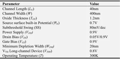
Table 2. Simulation Parameters used in TCAD Extraction of model (4) & (7).
Parameter Value
Channel Length (LG) 40nm
Channel Width (W) 400nm
Oxide Thickness (TOX) 1.2nm
Source surface built-in Potential (Ψbi) 0.7V
Subthreshold Swing (SS) 80mV/dec
Power Supply (VDD) 0.9V
Drain Bias (VDS) 0.05V/0.9V
Gate Bias (VGS) 0.9V
Minimum Depletion Width (WDM) 20nm
VTH Long-channel Device (VTH0) 0.8V
Operating Temperature (T) 300K
To elucidate and clarify the information, a physical model is proffered which also considers the short channel impacts, prominently, threshold voltage roll-off impact as the main cause for the inconsistent (VTH)-(IGL) relationship. The
physical components for the inconsistent relation between threshold voltage and gate leakage current are viewed as two-fold contrary operations:
1)Tunneling Gate leakage current density (JGL)
The surface potential reduces with the technology node as the oxide thickness is scaled. The tunneling gate leakage current density (JGL) diminishes with VTH over surface
potential (ψs) similarly as shown in BSIM4 model [15]:
!"#$&'%( exp
,-./0 &'123&'∅56
789|$&'| ; #1 < = 6 >(;
?2 @∅5 #|$&'|.∅5
∅5A B 1(
C
DE (2)
The variables A and B are used for the simplified representation of the complicated gate leakage current density equation. The variables are equated as:
F7
8HI∅JKLM N O = P1 <
| LM|
∅J Q
The auxiliary function Ninv represents the density of carriers in inversion layer of channel. It can be represented as:
!" R&'&' SS T U1 B FVW #$ %.$^^XYZ[\](_ (3)
Using (3) in (2), the gate leakage current density can be approximated as:
T `1 B FVW P ^<SS Za ]Qb
cZ∅J, KLM, eLM, LM, LM, ^, e] (4)
Here the values of the functions f, α, β are dependent barrier height (Φb), dielectric constant (εOX), electron effective mass
in the dielectric (mOX), dielectric thickness (TOX), operating
temperature (T), gate voltage (VGS), and overdrive voltage
across the dielectric (VOX). SS is the Subthreshold Swing.
2)Threshold Voltage roll-off impact (VTH roll-off)
threshold voltage roll-off impact. Threshold Voltage roll-off impact causes higher VTH for longer channel length (LG)
devices. As elaborated in [16], this impact can be compactly modeled as:
∆ < Za ] (5)
∆ 2g &'
hi jaJ ZaJ B k^] exp Z<
0 ⁄2
hil7 &'] (6)
From (5) and (6), the gate length and the threshold voltage relation can be presented as:
m n ln q$XYA.$rXYZ[\]E (7)
Here the values of η, γ variables are dependent on TOX, VDS,
the minimum depletion width WDM, and the source-substrate
built-in potential ψbi. VTH0 is the long-channel device threshold
voltage.
The net gate leakage current can be represented as:
m s (8) Figure. 3 illustrates the proffered model (4) and (7) for the inconsistent relation between threshold voltage and gate leakage current for nanoscaled MOSFETs. The gate leakage current (IGL) is adjusted between the previously mentioned
two contrary functions of VTH. For a particular device design
lot, the incline of IGL versus VTH variance relies on the initial
VTH position. The slope may alter from positive to negative as
elucidated through plotted TCAD simulation results. The simulation parameters used in the TCAD extraction of model (4) and (7) are listed in Table II. Figure. 3 evidently demonstrates typical standardized simulation results of the correlation of gate leakage (IGL), gate leakage current density
(JGL), channel length (LG) with threshold voltage (VTH) in
reference to the model (4) and (7).
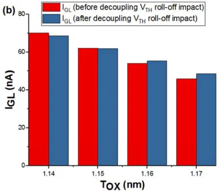
Figure 4. Demonstration of the relationship of VTLIN and IGL with TOX variance
when separating the VTH1 device design lot by estimated LG = 40nm, showing
that LER prompted threshold voltage roll-off impact overwhelms over the OTV impact. (a) VTLIN variance outwardly shows no association with oxide
thickness (TOX) when line-edge roughness (LER) induced threshold voltage
roll-off variation is considered. However, the VTLIN variance shows positive
association to the oxide thickness (TOX). (b) The gate leakage current (IGL)
shows steady negative relation to oxide thickness (TOX) before and after
decoupling threshold voltage roll-off impact.
4. Proffered Model Validation
For the proffered model validation of (4) and (7), we test the essential factors that influence the intrinsic device inconstancy regarding the (VTH)-(IGL) relationship by experimentally
decoupling the impacts of Random Dopant Fluctuation (RDF), Line-Edge Roughness (LER), and atomic-scale Oxide Thickness Variation (OTV) [1]. For the devices with the size of 400nm×10×40nm, a moderately little RDF-initiated σVTH ≈
2.5mV is assessed in view of the TCAD simulation [4]. To assess LER and OTV independently, we channel the experimental results considering the gate length and oxide thickness. Figure. 4 demonstrates the relationship of VTLIN and
TOX variance when separating the VTH1 device design lot by
estimated LG=40nm, displaying that LER prompted threshold
voltage roll-off impact overwhelms over the OTV impact. Figure. 4(a) demonstrates the VTLIN variance shows outwardly
no association with oxide thickness (TOX). when line-edge
roughness (LER) induced threshold voltage roll-off variation is considered. However, the VTLIN variance shows positive
association to the oxide thickness (TOX). Figure. 4(b) presents
the fact that the gate leakage current (IGL) shows steady
negative relation to oxide thickness (TOX). Hence, we can
conclude that the critically observed IGL versus VTLIN
Figure 5. Gate leakage current versus VTLIN variance (a) after decoupling
LER prompted threshold voltage roll-off impact by categorizing the device design lot (VTH1 – VTH4) with same channel length characteristics of Lg = 40nm
and (b) after decoupling the dielectric thickness variance by categorizing the device design lot (VTH1 – VTH4) with same dielectric thickness (Tox = 1.16nm)
devices.
Figure. 5(a) demonstrates the correlation of IGL versus VTLIN
after decoupling LER-prompted threshold voltage roll-off impact by categorizing the device design lot (VTH1 – VTH4) with
same channel length characteristics of LG= 40nm. Similarly,
Figure. 5(b) demonstrates the correlation of IGL versus VTLIN
subsequent to the decoupling the OTV impact categorizing the device design lot (VTH1 – VTH4) with same dielectric thickness
of TOX = 1.16nm. Observing the characteristics of the slope of
(IGL)-(VTLIN) curve for discrete threshold voltage device design
lots plotted in Figure. 5(a) and Figure. 5(b), we perceive unexpected inverse patterns, validating that threshold voltage roll-off impact plays a noteworthy part in the inconsistent threshold voltage dependent relationship between IGL and
VTLIN variance especially for nanoscaled devices. The
statement also supports the illustrations shown in Figure. 2. The results are also in agreement with the proffered model (4) and (7).
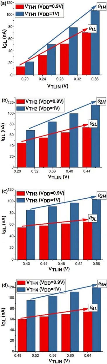
Figure 6. The rate of accretion of the gate leakage current vs. threshold voltage curve escalates with the increase in the power supply voltage (a)-(d) The plots illustrate that when VDD increases from 0.9V to 1V, the slope of
Table 3. Rate of Accretion of Gate Leakage Current vs. Threshold Voltage.
Parameter ӨL (VDD=0.9V) ӨH (VDD=1V)
VTH1 3.78e-7 5.68e-7
VTH2 1.91e-7 3.18e-7
VTH3 6.53e-8 1.24e-7
VTH4 9.14e-8 1.61e-7
The rate of accretion of the gate leakage current vs. threshold voltage curve escalates with the increase in the power supply voltage. Figure. 6(a)-(d) additionally demonstrates the (IGL)-(VTLIN) plot slope, SGL=d (IG)/d(VTLIN) increments with the
supply voltage for all the device design lot (VTH1 – VTH4), which
is in concurrence with the proffered model (4) and (7). It presents the comparative TCAD simulation results of the gate leakage slope for VDD = 0.9V and VDD = 1V in the bar graph
format. The rate of accretion of log (IGL) vs. VTH variations for
discrete design lot (VTH1 to VTH4) is respectively represented by
Ө1 to Ө4. The added subscript L/H corresponds to low/high
power supply i.e. VDD=0.9V/1V. For precise and specific
results, Table III represents the simulation outcomes in tabular format. It is clearly observed that the slope of (IGL)-(VTLIN) plot
increases for all four types of device designs.
5. Conclusion
The manuscript exhibited and proffered a physical model on the inconsistent relationship between the gate leakage current and threshold voltage variance precisely for nano scaled MOSFETs. The study and analysis presented in the manuscript has not been presently implemented in conventional gate leakage device models. The experimental results and the outcomes cannot be clarified by previously presented gate leakage models which attribute the evident threshold voltage variance to gate leakage current flowing through the gate resistance. Rather, the manuscript explores that the threshold voltage and gate leakage current (VTH)-(IGL) characteristics can
be precisely clarified and justified by short-channel impacts, in particular, the threshold voltage roll-off impact, along with a surface potential dependent gate leakage model. The tunneling gate leakage current density (JGL) diminishes with VTH over
surface potential (ψs). However, the threshold voltage roll-off
impact causes higher VTH for larger channel length (LG) devices.
The net gate leakage current is adjusted by these two contrary functions of threshold voltage. In addition, the rate of accretion of the gate leakage current with threshold voltage variation is also analyzed. The impact of the increase in the power supply voltage on the rate of accretion of the gate leakage current vs. threshold voltage curve is also explored. Thorough methodical TCAD simulations were accomplished to validate the proffered models. Both the experimental outcomes, TCAD simulations and physics based models were implemented to uncover and clarify the Threshold voltage and gate leakage relationship, particularly for nano MOSFETs. The future nano device models ought to envelop these inconsistent (VTH)-(IGL)
characteristics enlightened in this comprehensive study to enhance the precision of gate leakage current in power proficient, multi-threshold voltage circuit design and reliability analysis.
References
[1] Roy, Gareth, et al. "Simulation study of individual and combined sources of intrinsic parameter fluctuations in conventional nano-MOSFETs." IEEE Transactions on Electron Devices 53.12 (2006): 3063-3070.
[2] Wang, Xingsheng, et al. "Statistical threshold-voltage variabiliy in scaled decananometer bulk HKMG MOSFETs: A full-scale 3-D simulation scaling study." IEEE Transactions on Electron Devices 58.8 (2011): 2293-2301.
[3] Swami, Yashu, and Sanjeev Rai. "Modeling, Simulation, and Analysis of Novel Threshold Voltage Definition for Nano-MOSFET." Journal of Nanotechnology 2017 (2017). [4] Lundstrom, Mark, and Zhibin Ren. "Essential physics of carrier
transport in nanoscale MOSFETs." IEEE Transactions on Electron Devices 49.1 (2002): 133-141.
[5] Chang, Leland, et al. "Practical strategies for power-efficient computing technologies." Proceedings of the IEEE 98.2 (2010): 215-236.
[6] Kanj, Rouwaida, et al. "Design considerations for PD/SOI SRAM: Impact of gate leakage and threshold voltage variation." IEEE Transactions on Semiconductor Manufacturing 21.1 (2008): 33-40.
[7] Liu, Zihong, et al. "An anomalous correlation between gate leakage current and threshold voltage fluctuation in advanced MOSFETs." Electron Devices Meeting (IEDM), 2010 IEEE International. IEEE, 2010.
[8] Swami, Yashu, and Sanjeev Rai. "Modeling and analysis of sub-surface leakage current in nano-MOSFET under cutoff regime." Superlattices and Microstructures 102 (2017): 259-272.
[9] De Gyvez, J. Pineda, and Hans P. Tuinhout. "Threshold voltage mismatch and intra-die leakage current in digital CMOS circuits." IEEE Journal of Solid-State Circuits 39.1 (2004): 157-168.
[10] Koh, Meishoku, et al. "Limit of gate oxide thickness scaling in MOSFETs due to apparent threshold voltage fluctuation induced by tunnel leakage current." IEEE Transactions on Electron Devices 48.2 (2001): 259-264.
[11] Iyer, Subramanian S., and Edward J. Nowak. "45 nm SOI and beyond-getting to a general purpose technology." SOI Conference, 2007 IEEE International. IEEE, 2007.
[12] Narasimha, S., et al. "High performance 45-nm SOI technology with enhanced strain, porous low-k BEOL, and immersion lithography." Electron Devices Meeting, 2006. IEDM'06. International. IEEE, 2006.
[13] Swami, Yashu, and Sanjeev Rai. "Comparative methodical assessment of established MOSFET threshold voltage extraction methods at 10-nm technology node." Circuits and Systems 7.13 (2016): 32.
[15] Lee, Wen-Chin, and Chenming Hu. "Modeling CMOS tunneling currents through ultrathin gate oxide due to conduction-and valence-band electron and hole tunneling." IEEE Transactions on Electron Devices 48.7 (2001): 1366-1373.
[16] Taur, Yuan, and Tak H. Ning. Fundamentals of modern VLSI devices. Cambridge university press, 2013.
Biography
Yashu Swami, Senior Research Fellow is pursuing his Ph.D. in the field of Low Power Nano Device Modeling from the Department of Electronics & Communication Engineering, MNNIT Allahabad, India. He completed his M’Tech in VLSI Design with distinction from GGSIPU, New Delhi, India. He has more than ten years of experience in his field of research. He has more than 14 international publication in his research field with number of best paper awards.