doi: 10.11648/j.awcn.20190501.12
ISSN: 2575-5951 (Print); ISSN: 2575-596X (Online)
The Design of Three Phase Programmable Testing Power
Based on CPLD_DSP
Li Hui, Li Jing
Automated Institute, Huaiyin Institute of Technology, Huaian, China
Email address:
To cite this article:
Li Hui, Li Jing. The Design of Three Phase Programmable Testing Power Based on CPLD_DSP. Advances in Wireless Communications and Networks. Vol. 5, No. 1, 2019, pp. 13-18. doi: 10.11648/j.awcn.20190501.12
Received: August 3, 2019; Accepted: August 19, 2019; Published: September 3, 2019
Abstract:
A design of three phases programmable testing power program-controlled based on CPLD_DSP was introduced in the paper. RAM was driven and six DDS were generated in CPLD. RAM was driven and six DDS (three voltage signal and three current signal) were generated in CPLD. The six DDS signal was used as based signal of testing power. CPLD was programmed to control serial D/A chip named LTC1595B to adjust the value of voltage and current. Voltage signal and current signal were collected and computed and closed loop by DSP. After testing, the output frequency resolution of the system achieved 0.001Hz.The voltage and current control precision achieved 0.02%.Keywords:
Testing Power, CPLD, DDS, Output Precision1. Introduction
The programmable precision test power supply adopted direct frequency synthesis (DDS) technology. The high-precision standard power source was composed of CPLD, DSP, high-speed high-precision DA and high-fidelity power amplifier which was widely used in electrical measurement, thermal engineering, etc. of power systems. Instrumentation field [1-15]. The test power could output high-precision voltage and current with adjustable
frequency (40-65Hz) frequency, phase and amplitude, and was a high-precision adjustable voltage and current standard source.
2. System Overall Plan
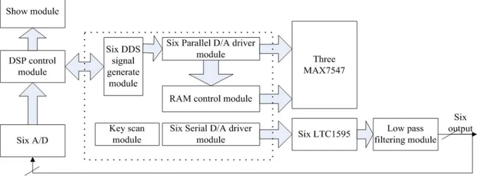
The system was mainly composed of DSP and CPLD minimum system and peripheral control circuit. The overall design block diagram of the system is shown in figure 1.
3. Hardware Design of the System
The hardware circuit was mainly composed of 6 serial A/D and channel switching circuits, parallel D/A and low-pass filter modules, serial D/A control module, RAM control and other major modules. The following described the main modules.
3.1. Serial A/D Sampling and Channel Switching Module
The specific circuit was shown in figure 2. This design circuit was mainly used to collect the 6-channel feedback voltage and current signals. The MAX1132 serial A/D chip was combined with the multi-channel selector MAX308 to realize 6-channel time-sharing sampling.
Figure 2. Serial A/D sampling and channels switching circuit.
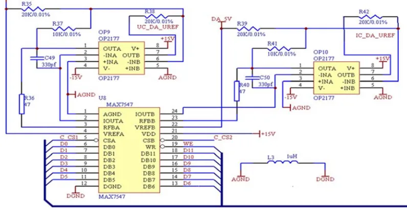
3.2. Parallel D/A Conversion Module
Parallel D/A conversion mainly used MAX7547 which was driven by CPLD. 6 reference signals generated by DDS were converted. MAX7547 could complete D/A conversion of 2 signals by time-sharing conversion. MAX7547 was current type D/A. The
output from MAX7547 would be converted into the bipolar voltage output signal. The specific circuit was shown in figure 3. For the 6-channel signal, three MAX7547s were required, which were connected in parallel and 6-way time-sharing. The specific timing was designed by the state machine of the CPLD.
3.3. Serial D/A Control Module
The serial D/A control module used LTC1595 control chip which was driven by the CPLD to realize serial timing in the state machine. Such hardware wiring circuits were more conventional and would not be discussed this time.
4. System Software Design and Circuit
Simulation
The software part mainly included two parts of DSP and CPLD. This paper focused on the program design and circuit simulation of CPLD.
4.1. DSP Part Software Design
Figure 4. DSP part software flow chart.
The DSP part was mainly composed of A/D sampling module, and CPLD communication module, LCD display and
closed-loop control. The specific control flow chart was shown in figure 4.
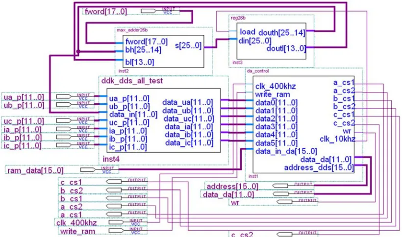
4.2. CPLD Part of the Software Design
The CPLD part mainly included 6 DDS waveform generation modules, DSP communication module, RAM control module, parallel D/A7547 driver module and serial D/A1595 driver module.
4.2.1. DDS Wave Form Generation Module Software Design
The system used direct frequency synthesis technology to generate six sinusoidal signals with adjustable frequency and phase, including frequency accumulator, phase accumulator, and data latch. The number of bits of the frequency accumulator directly determined the frequency resolution of the output signal [13-15], the system required the output to be 40 ~ 65Hz adjustable, the frequency resolution was 0.001HZ, the system selected the reference clock fs = 10KHZ, the resolution was fs/2N, Where N was the number of bits of the frequency accumulator [7], so if N=26 was selected, the actual frequency resolution should be 10000/226=0.00015Hz, and the adjustable frequency word range was from 41893 to 6A7F0 (40~65Hz). According to the frequency word range, the highest two bits of the selected 20-bit data were always "01", that was, from 0100 0001 1000 1001 0011 to 0110 1010 0111 1111 0000, so the frequency word only needed 18 lines, and the phase resolution required 0.1 degree. The phase resolution was 360/2M, where M was the number of bits of the phase accumulator, so the phase accumulator was selected as 12 bits [3], and the actual resolution is 360/212 = 0.088 degrees. The specific block diagram was shown in figure 5.
4.2.2. Communication Interface Module with DSP
This module mainly completed the communication interface with DSP. A total of 21 lines were selected. The highest-order DSP20 acted as a DSP to send command/data handshake control lines to the CPLD. When the DSP20 had a falling edge, the DSP sent commands and data to the CPLD. As the CPLD sent the command/data handshake control line to the DSP, the DSP19 was also valid for the falling edge. The first five lines of the other 19 lines were used as commands, and the last 14 bits were used as data, which was implemented in the process and used DSP20 as a sensitive signal. 4].
4.2.3. Parallel D/A Control Module
The parallel control module selected the MAX7547 and selected the state machine [3-6] to drive. The voltage signal after the conversion was used as the reference voltage of the serial D/A chip LTC1595. The MAX7547 contained two sets of 12-bit current-mode output D/A. The reference voltage was set to 5V. CSA, CSB, and WR were its main control terminals. DB11~DB0 were 12-bit parallel data inputs. Two analog signals were output from IOUTA and IOUTB respectively. The working principle was as follows:
The control terminals were active low, CSA, CSB were two sets of D/A chip select, D/A was time-sharing, WR was the conversion enable signal, first prepare the data to be converted,
then set the chip select to Low level, after a delay, the WR enable signal was pulled from the initial high level to low level, delayed for a period of time, after a conversion was completed, the WR was set to a high level, which caused it to fail and delayed for a period of time. After the chip select signal CSA (CSB) was restored to the initial high level, a D/A conversion was completed. The specific timing requirements could be referred to the MAX7547 chip manual.
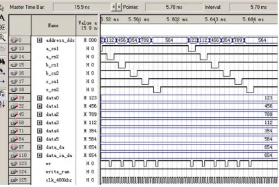
According to the above working principle, 1 channel D/A conversion was set to 5 states, 6 channels D/A time division D/A conversion was set to 40 states, 30 of which were legal, and the remaining 10 were illegal state, the state machine performed one-by-one conversion under the action of the clock. The clock of the state machine was 400KHZ, the period was 2.5 microseconds, and the completion of one channel D/A required 5 clock cycles of 12.5 microseconds, and the same way D/A twice. The D/A conversion interval was 40 clock cycles and 100 microseconds. Therefore, each DDS was designed to use the same clock 10KHZ (cycle 100 microseconds) to ensure that each data in the 6-channel DDS output data was kept at 100 microseconds to guarantee stable output of D/A data. The output after timing simulation of the module was shown in figure 6.
Figure 6. Parallel D/A module timing simulating diagram.
It could be seen from the figure that the chip selection CS and the write signal WR of the 6-channel D/A were sequentially valid, and the address signals of the DDS were also sequentially outputted. The data obtained by the RAM module was also sequentially output, and the RAM module was driven. It was relatively simple and would not be
introduced here.
4.2.4. Serial D/A Control Module
LD was the data latch terminal, and serial data was generated after D/A conversion was started. Under the action of the clock, data shift conversion was performed. After the rising edge of the 16th clock, the LD terminal level was pulled low, and the parallel data after the conversion was latched and a D/A conversion was completed. Therefore, the CPLD used the state machine to output the timing-compliant control signal, that was, first generated 16 conversion clock signals, one latch
signal, and the latch signal was initially high, latched after the rising edge of the 16th clock. The signal was pulled down to a low level, and the input 16-bit parallel data was shift-converted under the action of the clock, and converted into 1 serial data to the SRI serial data input end of LTC1595 for D/A conversion, specific circuit simulation timing diagram was shown in figure 7 [7-10].
Figure 7. Serial D/A controling module timing simulating diagram.
It could be seen from the simulation diagram that the set timing logic was matched, in which clk_10mhz was used as the conversion clock of the state machine, selected as 1MHZ, en was the work permission signal, data word was used as the parallel data input, and shift_clk was the output D/A conversion. Storage_clk was the output D/A latch control signal, and ds was the serial data output to the LTC1595.
5. Conclusion
RAM was driven and six DDS (three voltage signal and three current signal) were generated in CPLD. The six DDS signal was used as based signal of testing power, and CPLD was programmed to control serial D/A chip named LTC1595B to adjust the value of voltage and current. The main control CPLD chip of the system selected the MAXII series chip EPM1270T144C5, the resource utilization rate of the chip was less than 80%. The information collected from keyboard was sent to DSP. Wide-screen LCD was controlled by DSP to show data on line. Voltage signal and current signal were collected and computed and closed loop by DSP, and the same time controlling command was sent to CPLD. After the hardware test of the system, the system ran stably and could complete the given technical indicators well. The output frequency resolution was 0.0002. Hz,
phase resolution of 0.088 degrees, the output accuracy of voltage and current were up to 0.02%.
References
[1] Meng Shuai Qi, Xu Zhiping, Yin Xinyu, et al. Basic Principles of Signal Generator Based on DDS [J]. Science and Technology and Innovation, 2019 (09): 72-73.
[2] ZHANG Kai-lin, SU Shu-jing, LIU Li-sheng, et al. Design of Multi-channel DDS Signal Generator Based on FPGA [J]. Electrical Measurement & Instrumentation, 2011, 48, (03): 63-66.
[3] Anna Puiggalí-Jou, Luis J. del Valle, Carlos Alemán. Drug delivery systems based on intrinsically conducting polymers [J]. Journal of Controlled Release, 2019: 309.
[4] Wang Yan Feng. Digital Electronic Circuit and EDA Technology [M]. Beijing: Chemical Industry Press, 2011.
[5] Zhang Jing, Han Rui. EDA technology and application [M], Beijing: Tsinghua university press, 2018.
[6] Liu Jiang Hai. EDA technology [M]. Wuhan: Huazhong University of Science and Technology Press, 2013.
[8] LI Xue-mei, ZHANG Hong-cai, WANG Xue-wei. The Design of a Signal Source Based on DDS Technology [J]. Electrical Measurement & Instrumentation, 2010, 47 (01): 55-66.
[9] Li wen bing, Hao qiang, Du yuan bo, et al. Demonstration of a Sub-Sampling Phase Lock Loop Based Microwave Source for Reducing Dick Effect in Atomic Clocks [J]. Chinese Physics Letters, 2019, 36 (07): 23-26.
[10] WANG Hong-liang, HUANG Yang-wen. Design of Programmable Multi-signal Generator based on FPGA [J]. Fire Control & Command Control, 2010, 35, (06): 97-99.
[11] LIU Yuan, YU Ya-ping, WANG Hong-yi, LIU Hua, CHANG Ruo-kui. Design of the NC Signal Generator Based on FPGA [J]. Techniques of Automation and Applications, 2009, 28, (12): 75-77.
[12] He Wei, Lu Jintao, Li Jia, Wu Lina. The design of DDS with improved CORDIC method [J]. Application of Electronic. Technique, 2011, 37, (01): 65-67.
[13] Pan Shuolong. C-band frequency synthesis design based on DA and DDS technology [A]. China Electronics Society [C]. Proceedings of the 2019 National Microwave and Millimeter Wave Conference (Volume 1). China Electronics Society: Microwave Branch of China Electronics Society, 2019: 3.
[14] Hui Fei. Development and Example of Embedded System Based on FPGA [M]. Xi An, Xidian University Press, 2017.