IJEDR1704043
International Journal of Engineering Development and Research (
www.ijedr.org
)
281
Design Of Carry Skip Adder Using High Speed Skip
Logic In Xilinx Platform
P. Prabakaran, B. Theeban Chakkaravarthy, G. Manikannan Department of ECE
CK College of Engineering & Technology, Cuddalore, India
________________________________________________________________________________________________________
Abstract—The portable equipment’s such as cellular phones, Personal Digital Assistant (PDA), and notebook personal computer, arise the need of effective circuit area and power efficient VLSI circuits. Addition is the most common and often used arithmetic operation in digital computers and also, it serves as a building block for synthesis all other arithmetic operations. The carry skip adder(CSKA) structure that has a higher speed yet lower energy consumption with the conventional one. The speed enhancement is achieved by applying cancatenation schemes improve the efficiency of the conventional CSKA(conv-CSKA) structure. In addition instead of utilizing multiplexer logic, the proposed structure makes use of AND-OR-invert(AOI) and OR-AND-invert(OAI) compound gates for the skip logic.
Keywords—carry skip adder, energy efficient, higher performance.
________________________________________________________________________________________________________
I. INTRODUCTION
Conventional CSKA is a RCA-RCA configuration which generates a pair of sum words and output-carry bits corresponding the anticipated input-carry (cin= 0 and 1), and selects one out of each pair for final-sum and final-output-carry. Conventional CSKA has less CPD than RCA, but the design is not attractive, since it uses dual RCA. Few attempt have been made to avoid dual use of RCA in CSKA design.
Adders are a key building block in arithmetic and logic units (ALUs) and hence increasing their speed and reducing their power/energy consumption strongly affect the speed and power consumption of processors[1]. There are many works on the subject of optimizing the speed and power of these units, which have been reported. Obviously, it is highly desirable to achieve higher speeds at low-power/energy consumptions, which is a challenge for the designers of general purpose processors. One of the effective techniques to lower the power consumption of digital circuits is to reduce the supply voltage due to quadratic dependence of the switching energy on the voltage. Moreover, the subthreshold current, which is the main leakage component in OFF devices, has an exponential dependence on the supply voltage level through the drain-induced barrier lowering effect. Depending
on the Amount of the supply voltage reduction, the operation of ON devices may reside in the superthreshold, near-threshold, or subthreshold regions.
Working in the superthreshold region provides us with lower delay and higher switching and leakage powers compared with the near/subthreshold regions. In the subthreshold region, the logic gate delay and leakage power exhibit exponential dependences on the supply and threshold voltages. Moreover, these voltages are (potentially) subject to process and environmental variations in the nanoscale technologies. The variations increase uncertainties in the aforesaid performance parameters. In addition, the small subthreshold Current causes a large delay for the circuits operating in the subthreshold region. Recently, the near-threshold region has been considered as a region that provides a more desirable tradeoff point between delay and power dissipation compared with that of the subthreshold one, because it results in lower delay compared with the subthreshold region and significantly lowers switching and leakage powers compared with the superthreshold region. In addition, near-threshold operation, which uses supply voltage levels near the threshold voltage of transistors, suffers considerably less from the process and environmental variations compared with the subthreshold region[3].
II.EXISTINGSYSTEM
It is possible to create a logical circuit using multiple full adders to add N-bit numbers. Each full adder inputs a Cin, which
is the Cout of the previous adder. This kind of adder is called a ripple-carry adder, since each carry bit "ripples" to the next full adder.
Note that the first (and only the first) full adder may be replaced by a half adder (under the assumption that Cin = 0).The layout of a
ripple-carry adder is simple, which allows for fast design time; however, the ripple-carry adder is relatively slow, since each full adder must wait for the carry bit to be calculated from the previous full adder. The structure of an N-bit Conv-CSKA, which is based on blocks of the RCA (RCA blocks), is shown in Fig 1. In addition to the chain of FAs in each stage, there is a carry skip logic. For an RCA that contains N cascaded FAs, the worst propagation delay of the summation of two N-bit numbers, A and B, belongs to the case where all the FAs are in the propagation mode. It means that the worst case delay belongs to the case where Pi = Ai ^Bi =1 for i = 1, . . . , N
where Pi is the propagation signal related to Ai and Bi. fig 1. Conventional CSKA structure
IJEDR1704043
International Journal of Engineering Development and Research (
www.ijedr.org
)
282
ready for the next stage without waiting for the operation of the FA chain to be completed. The skip operation is performed using the gates and the multiplexer shown in the figure. Based on this explanation, the N FAs of the CSKA are grouped in Q stages. Each stage contains an RCA block with Mj FAs ( j = 1, . . . , Q) and a skip logic. In each stage, the inputs of the multiplexer (skip logic) are the carry input of the stage and the carry output of its RCA block (FA chain). In addition, the product of the propagation signals (P) of the stage is used as the selector signal of the multiplexer. The CSKA may be implemented using FSS and VSS where the highest speed may be obtained for the VSS structure.
Existing system disadvantages:
A ripple carry adder is a logic circuit in which the carry-out of each full adder is the carry in of the succeeding next most significant full adder. It is called a ripple carry adder because each carry bit gets rippled into the next stage.
More area overhead system More power consumption Low speed architecture
III. Proposed Structure:
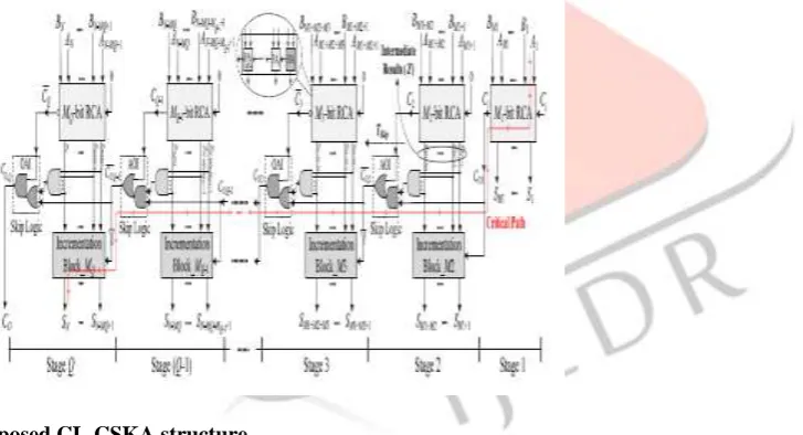
The structure is based on combining the concatenation and the incrementation schemes with the Conv-CSKA structure, and hence, is denoted by CI-CSKA. It provides us with the ability to use simpler carry skip logics. The logic replaces 2:1 multiplexers by AOI/OAI compound gates. The gates, which consist of fewer transistors, have lower delay, area, and smaller power consumption compared with those of the 2:1 multiplexer . Note that, in this structure, as the carry propagates through the skip logics, it becomes complemented. Therefore, at the output of the skip logic of even stages, the complement of the carry is generated. The structure has a considerable lower propagation delay with a
Fig 2. Proposed CI- CSKA structure
IJEDR1704043
International Journal of Engineering Development and Research (
www.ijedr.org
)
283
reason for using both AOI and OAI compound gates as the skip logics is the inverting functions of these gates in standard cell libraries.This way the need for an inverter gate, which increases the power consumption and delay, is eliminated. As shown in Fig. 2, if an AOI is used as the skip logic, the next skip logic should use OAI gate. In addition, another point to mention is that the use of the proposed skipping structure in the Conv-CSKA structure increases the delay of the critical path considerably. This originates from the fact that, in the Conv-CSKA, the skip logic (AOI or OAI compound gates) is not able to bypass the zero carry input until the zero carry input propagates from the corresponding RCA block. To solve this problem, in the proposed structure RCA block with a carry input of zero (using the concatenation approach). This way, since the RCA block of the stage does not need to wait for the carry output of the in parallel.
Area and Delay of the Proposed Structure:
As mentioned before, the use of the static AOI and OAI gates (six transistors) compared with the static 2:1 multiplexer (12 transistors), leads to decreases in the area usage and delay of the skip logic [37], [38]. In addition, except for the first RCA block, the carry input for all other blocks is zero, and hence, for these blocks, the first adder cell in the RCA chain is a HA. This means that (Q − 1) FAs in the conventional structure are replaced with the same number of HAs in the suggested structure decreasing the area usage (Fig. 2). In addition, note that the proposed structure utilizes incrementation blocks that do not exist in the conventional one. These blocks, however, may be implemented with about the same logic gates (XOR and AND gates) as those used for generating the select signal of the multiplexer in the conventional structure. Therefore, the area usage of the proposed CI-CSKA structure is decreased compared with that of the conventional one. The critical path of the proposed CI-CSKA structure, which contains three parts, is shown in Fig. 2. These parts include the chain of the FAs of the first stage, the path of the skip logics, and the incrementation block in the last stage. The delay of this path (TD) may be expressed as
where the three brackets correspond to the three parts mentioned above, respectively. Here, TAND and TXOR
are the delays of the two inputs static AND and XOR gates, respectively. Note that, [(Mj − 1)T AND + TXOR] shows the
critical path delay of the j th incrementation block (TINC, j ), which is shown in Fig. 3. To calculate the delay of the skip logic, the average of the delays of the AOI and OAI gates, which are typically close to one another is used. Thus above equation may be modified to
Stage Sizes Consideration:
Similar to the Conv-CSKA structure, the proposed CI-CSKA structure may be implemented with either FSS or VSS. Here, the stage size is the same as the RCA and incrementation blocks size. In the case of the FSS (FSS-CI-CSKA), there are Q = N/M stages with the size of M. The optimum value of M, which may be obtained using (11), is given by Mopt = N(TAOI + TOAI) 2(TCARRY + TAND) . (12) In the case of the VSS (VSS-CI-CSKA), the sizes of the stages, which are M1 to MQ, are obtained using a method similar to the one discussed in Section III-B. For this structure, the new value for TSKIP should be used, and hence, α becomes (TAOI+TOAI) / (2×TCARRY). In particular, the following steps should be taken.
1) The size of the RCA block of the first stage is one.
2) From the second stage to the nucleus stage, the size of j th stage is determined based on the delay of the product of the sum of its RCA block and the delay of the carry output of the ( j − 1)th stage. Hence, based on the description given in Section III-B, the size of the RCA block of the j th stage should be as large as possible, while the delay of the product of the its output sum should be smaller than the delay of the carry output of the ( j − 1)th stage. Therefore, in this case, the sizes of the stages are either not changed or increased.
IJEDR1704043
International Journal of Engineering Development and Research (
www.ijedr.org
)
284
4) Starting from the stage (p + 1) to the last stage, the sizes of the stage i is determined based on the delay of the incrementation block of the i th and (i − 1)th stages (TINC,i and TINC,i−1, respectively), and the delay of the skip logic. In particular TINC,i ≤ TINC,i−1 − TSKIP,i−1; for i ≥ p + 1. In this case, the size of the last stage is one, and its RCA block contains a HA.5) Finally, note that, it is possible that the sum of all the stage sizes does not become equal to N. In the case, where the sum is smaller than N by d bits, that should add another stage with the size of d. The stage is placed close to the stage with the same size. In the case, where the sum is larger than N by d bits, the size of the stages should be revised(Step 3).Now, the procedure for determining the stage sizes is demonstrated for the 32-bit adder. It includes both the conventional and the proposed CI-CSKA structures. The number of stages and the corresponding size for each stage, which are given in Fig. 4, have been determined based on a 45-nm static CMOS technology. The dashed and dotted lines in the plot indicate the rates of size increase and decrease. While the increase and decrease rates in the conventional structure are balanced, the decrease rate is more than the increase one in the case of the proposed structure. It originates from the fact that, in the Conv-CSKA structure, both of the stages size increase and decrease are determined based on the RCA block delay , while in the proposed CI-CSKA structure, the increase is determined based on the RCA block delay and the decrease is determined based on the incrementation block delay. The imbalanced rates may yield a larger nucleus stage and smaller number of stages leading to a smaller propagation delay[4].
Proposed hybrid variable latency CSKA:
In this section, first, the structure of a generic variable latency adder, which may be used with the voltage scaling relying on adaptive clock stretching, is described. Then, a hybrid variable latency CSKA structure based on the CI-CSKA structure described as follow.
Variable Latency Adders Relying on Adaptive Clock Stretching:
The basic idea behind variable latency adders is that the critical paths of the adders are activated rarely. Hence, the supply voltage may be scaled down without decreasing the clock frequency. If the critical paths are not activated, one clock period is enough for completing the operation. In the cases, where the critical paths are activated, the structure allows two clock periods for finishing the operation. Hence, in this structure, the slack between the longest off-critical paths and the longest critical paths determines the maximum amount of the supply voltage scaling. Therefore, in the variable latency adders, for determining the critical paths activation, a predictor block, which works based on the inputs pattern, is required. The concepts of the variable latency adders, adaptive clock stretching, and also supply voltage scaling in an N-bit RCA adder may be explained using Fig. 5. The predictor block consists of some XOR and AND gates that determines the product of the propagate signals of considered bit positions. Since the block has some area and power overheads, only few middle bits are used to predict the activation of the critical paths at price of prediction accuracy decrease. The input bits ( j + 1)th–( j + m)th have been exploited to predict the propagation of the carry output of the j th stage (FA) to the
carry output of (j+m)th stage.
IJEDR1704043
International Journal of Engineering Development and Research (
www.ijedr.org
)
285
Fig 4. Generic structure of variable latency adders based on RCAand the carry propagation path from ( j +1)th stage to the Nth stage (which are denoted by Short Latency Path (SLP1) and SLP2, respectively) are the longest off-critical paths. It should be noted the paths that the predictor shows are (are not) active for a given set of inputs are considered as critical (off-critical) paths. Having the bits in the middle decreases the maximum of the off-critical paths. The range of voltage scaling is determined by the slack time, which is defined by the delay difference between LLP and max(SLP1, SLP2). Since the activation probability of the critical paths is low (<1/2m), the clock stretching has a negligible impact on the throughput (e.g., for a 32-bit adder, m = 6–10 may be considered. There are cases that the predictor mispredicts the critical path activation. By increasing m, the number of misprediction decreases at the price of increasing the longest off-critical path, and hence, limiting the range of the voltage scaling. Therefore, the predictor block size should be selected based on these tradeoffs.
Proposed Hybrid Variable Latency CSKA Structure:
The basic idea behind using VSS CSKA structures was based on almost balancing the delays of paths such that the delay of the critical path is minimized compared with that of the FSS structure.
This deprives us from having the opportunity of using the slack time for the supply voltage scaling. To provide the variable latency feature for the VSS CSKA structure, the replace some of the middle stages in our proposed structure with a PPA is modified . It should be noted that since the Conv-CSKA structure has a lower speed than that of the
Fig 5. Proposed hybrid variable latency CSKA structure
IJEDR1704043
International Journal of Engineering Development and Research (
www.ijedr.org
)
286
is shown. Note that, for this figure, the size of the PPA is assumed to be 8 (i.e., Mp = 8). As shown in the figure, in the preprocessing level, the propagate signals (Pi ) and generate signals (Gi ) for the inputs are calculated. In the next level, using Brent–Kung parallel prefix network, the longest carry (i.e., G8:1) of the prefix network along with P8:1, which is the product of the all propagate signals of the inputs, are calculated sooner than other intermediate signals in this network. The signal P8:1 is used in the skip logic to determine if the carry output of the previous stage (i.e., CO,p−1) should be skipped or not. In addition, this signal is exploited as the predictor signal in the variable latency adder. It should be mentioned that all of these operations are performed in parallel with other stages. In the case, where P8:1 is one, CO,p−1 should skip this stage predicting that some critical paths are activated. On the other hand, when P8:1 is zero, CO,p is equal to the G8:1. In addition, no critical path will be activated in this case. After the parallel prefix network, the intermediate carries, which are functions of CO,p−1 and intermediate signals, are computed. Finally, in the post processing level, the output sums of this stage are calculated. It should be noted that this implementation is based on the similar ideas of the concatenation and incrementation concepts used in the CI-CSKA discussed. It should be noted that the end part of the SPL1 path from CO,p−1 to final summation results of the PPA block and the beginning part ofthe SPL2 paths from inputs of this block to CO,p belong to the PPA block. In addition. similar to the proposed CI-CSKA structure, the first point of SPL1 is the first input bit of the first stage, and the last point of SPL2 is the last bit of the sum outp ut of the incrementation block of the stage Q. The steps for determining the sizes of the stages in the hybrid variable latency CSKA structure are similar to the ones discussed. Since the PPA structure is more efficient when its size is equal to an integer power of two and select a larger size for the nucleus stage accordingly. This implies that the third step discussed in that section is modified. The larger size (number of bits), compared with that of the nucleus stage in the original CI-CSKA structure, leads to the decrease in the number of stages as well smaller delays for SLP1 and SLP2.
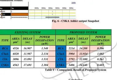
Simulation results:
Fig. 6 - CSKA Adder output Snapshot
EXISTING SYSTEM PROPOSED SYSTEM TYPE AREA
µm2 DELAY (ns) POWER DISSIPATION (mW)
TYPE AREA µm2 DELAY (ns) POWER DISSIPATION (mW) RCA 4526 16.907 1.548 RCA 2214 14.208 0.206 CSaA 6820 11.987 2.134 CSaA 5904 13.924 1.082 CIA 3096 15.891 1.531 CIA 2793 12.880 0.261 CSKA 4563 17.691 2.304 CSKA 3486 14.640 0.603
Table 1 – Comparison Result of Proposed System
Conclusion
A new adder named CI-CSKA will achieve high speed computation with less power consumption. By this design the overall chip area will be reduces at greater extent to that of conventional carry skip adder.Based on the discussion presented it is concluded that by reducing the delay of the skip logic, one may lower the propagation delay of the CSKA significantly. when modified CSKA structure that reduces this delay.
Reference
[1] I. Koren, Computer Arithmetic Algorithms, 2nd ed. Natick, MA, USA: A K Peters, Ltd., 2002.
[2] ] R. Zlatanovici, S. Kao, and B. Nikolic, “Energy–delay optimization of 64-bit carry-lookahead adders with a 240 ps 90 nm CMOS designexample,” IEEE J. Solid-State Circuits, vol. 44, no. 2, pp. 569–583, Feb. 2009.
[3] S. K. Mathew, M. A. Anders, B. Bloechel, T. Nguyen, R. K. Krishnamurthy, and S. Borkar, “A 4-GHz 300-mW 64-bit integer execution ALU with dual supply voltages in 90-nm CMOS,”IEEE J. Solid-State Circuits, vol. 40, no. 1, pp. 44–51, Jan. 2005. [4] V. G. Oklobdzija, B. R. Zeydel, H. Q. Dao, S. Mathew, and R. Krishnamurthy, “Comparison of high-performance VLSI adders
in the energy-delay space,” IEEE Trans. Very Large Scale Integr. (VLSI) Syst., vol. 13, no. 6, pp. 754–758, Jun. 2005. [5] B. Ramkumar and H. M. Kittur, “Low-power and area-efficient carry select adder,” IEEE Trans. Very Large Scale Integr.
(VLSI) Syst., vol. 20, no. 2, pp. 371–375, Feb. 2012.
[6] M. Vratonjic, B. R. Zeydel, and V. G. Oklobdzija, “Low- and ultra low-power arithmetic units: Design and comparison,” in Proc. IEEE Int. Conf. Comput. Design, VLSI Comput. Process. (ICCD), Oct. 2005, pp. 249–252.
IJEDR1704043
International Journal of Engineering Development and Research (
www.ijedr.org
)
287
[8] Y. He and C.-H. Chang, “A power-delay efficient hybrid carry lookahead/ carry-select based redundant binary to two’scomplement converter,” IEEE Trans. Circuits Syst. I, Reg. Papers, vol. 55, no. 1, pp. 336–346, Feb. 2008.
[9] C.-H. Chang, J. Gu, and M. Zhang, “A review of 0.18 μm full adder performances for tree structured arithmetic circuits,” IEEE Trans. Very Large Scale Integr. (VLSI) Syst., vol. 13, no. 6, pp. 686–695, Jun. 2005.
[10] D. Markovic, C. C. Wang, L. P. Alarcon, T.-T. Liu, and J. M. Rabaey, “Ultralow-power design in near-threshold region,” Proc. IEEE, vol. 98, no. 2, pp. 237–252, Feb. 2010.
[11] R. G. Dreslinski, M. Wieckowski, D. Blaauw, D. Sylvester, and T. Mudge, “Near-threshold computing: Reclaiming Moore’s law through energy efficient integrated circuits,” Proc. IEEE, vol. 98, no. 2, pp. 253–266, Feb. 2010.