1 |
P a g e
MODIFIED GDI TECHNIQUE - A POWER EFFICIENT METHOD FOR
DIGITAL CIRCUIT DESIGN
Pankaj Verma
1, Ruchi Singh
2and Y. K. Mishra
3 1Department of Electronics and Communication Engineering, BBDNIIT, LUCKNOW, INDIA 2Department of Electronics and Communication Engineering, BBDNITM, LUCKNOW, INDIA
3 Department of Electronics Engineering, KNIT, SULTANPUR, INDIA
ABSTRACT:
This paper presents logic style comparisons based on different logic functions and claimed modified Gate Diffusion Input logic (Mod-GDI) to be much more power-efficient than Gate Diffusion Input logic (GDI) and complementary CMOS logic design. However, DC and Transient analysis performed on more efficient modified Gate Diffusion Input logic (Mod-GDI) circuit realizations and a wider range of different logic cells, as well as the use of practical circuit arrangements reveal Mod-GDI to be superior to GDI and CMOS in the majority cases with respect to speed, area, power dissipation, and power-delay products. This manuscript shows that Mod-GDI is the logic style of preference for the realization of arbitrary combinational circuits, if low voltage, low power, and small power-delay products are of concern. All Simulations are performed through PSPICE based on 0.18μm CMOS technology, and results show power characteristics of Mod-GDI technique of low power digital circuit design. Simulation results shows up to 45% reduction in power-delay product in Mod-GDI. Mod-GDI approach allows realization of a broad variety of multifaceted logic functions by means of only two transistors. This technique is appropriate for designing of fast, low power circuits, using reduced number of transistor (as compared to CMOS techniques), while improving power characteristics.KEYWORD: Low power, Power minimization, Ultra low power VLSI circuits, Logic style, CMOS, GDI, Mod-GDI,
and Logic gates, AND, OR, MUX, digital circuits, DC analysis, transient response.I.INTRODUCTION
Among the forceful investigation in the field of low power, high speed digital applications due to the growing demand of systems like phones, laptop, palmtop computers, cellular phones, wireless modems and portable multimedia applications etc has directed the VLSI technology to scale down to nano-regimes, allowing additional functionality to be incorporated on a single chip. The designer‟s novel purpose in the field of multifaceted digital circuit design is minimization of power consumption. These investigations are responsible for special design techniques for digital circuits distant from conventional CMOS design style. A large body of investigate has been performed to expand and advance conventional Complementary Metal Oxide Semiconductor (CMOS) techniques for the fabrication of ULTRA low power integrated circuits (ICs). The purpose of this study is to expand a faster, lower power, and reduced area substitute to standard CMOS logic circuits. Mod-GDI technique is one such new technique for minimization of power consumption in the digital circuit design field[1,2,3].
2 |
P a g e
For the period of the last two decades investigation has resulted in the progress of numerous logic design techniques. An alternative approach to CMOS logic design is pass-transistor logic (PTL) design having advantages over standard CMOS design, these are: high speed which results from the small node capacitances; low power dissipation which results from the reduced number of transistors used in fabrication; and lower interconnection effects which results from small area. But there were also some basic problems in PTL realizations; i) the threshold drop across the single-channel pass transistors which results in reduced current drive and therefore slower function at reduced supply voltages [1]. This threshold voltage drop is significant for low power design because it is advantageous to function at the lowest possible voltage level. ii) In view of the fact that the input voltage for a high logic level at the regenerative inverters is not VDD, the PMOS device in the inverter is not fully turned off, and for this reason direct-path static power dissipation can be important. After that many investigations have performed to resolve these problems which results in techniques like: Transmission Gate CMOS (TG), Complementary Pass-transistor Logic (CPL), and Double Pass-transistor Logic (DPL).Transmission Gate CMOS (TG) logic; Complex logic functions are realized using transmission gate logic with the help of small number of complementary transistors This logic style eliminate the problem of low logic level swing as a result of using PMOS as well as NMOS transistors.
Complementary Pass-transistor Logic (CPL); this logic style presents complementary inputs/outputs by using NMOS pass-transistor logic with CMOS output inverters. The small stack height as well as the internal node low swing is CPL's mainly vital characteristic which contributes to lowering the power consumption. Drawback of this logic style was static power consumption results from the low swing at the gates of the output inverters. To eliminate this drawback of the power consumption, latched complementary pass-transistor logic (LCPL) and swing restored pass-transistor logic (SRPL) circuit styles be used at the place of CPL logic which have PMOS restoration transistors or cross-coupled inverters correspondingly.
Double Pass-transistor Logic (DPL); full swing process is performed with the help of complementary transistors to carry on and reduce the DC power consumption, which eliminates the need for restoration circuitry. There was also one deficiency that is the large area constraint by means of the subsistence of PMOS transistors.
Apart from all these there was an additional difficulty with PTL logic style that is the top-down logic design complication, which prevents the PTL logic style from playing a key responsibility in real logic large-scale integration technology (LSI).
All above logic style were used for designing of synchronous circuits but there were some problems so Asynchronous logic design has been recognized as an aggressive substitute to synchronous circuits. These Asynchronous logic designs acclaim to the potential for low-power, high-speed, reduced electromagnetic interference. Asynchronous logic has been developed in the last decade in the direction of transaction with the challenges posed by the advancement of very large-scale integration (VLSI) design, jointly by the high density, greater than ever number of gates on chip, and GHz frequencies of operation. But when operating at the 10 GHz frequencies difficulties are predictable towards future high-performance technologies which results from the enlarged impact of interconnect on signal delay, ambiguity in the delay of a gate, and on-chip parameter variations. These factors create difficulties in the design of fast digital systems controlled by a single general clock, due to considerations of delay skew between distant logic blocks, as well as the complexity of design of structures controlled by multiple clocks. The key features of systems based on Asynchronous design are self-timed circuits, which require no control of a general clock, alongside speedy communication protocols in which speed depends just on the self delay of the logic gates. The nonexistence of a general clock is the most important characteristics of Asynchronous design which contributes to low power operation, by means of eliminating the intense power consumption of definite chip areas where several transactions occur with arrival of each clock signal[2].
On the other hand, these attractive characteristics of Asynchronous digital circuit design typically come at a cost of either silicon area, or speed, or power, and cannot be achieved all at once. In addition, asynchronous circuits are usually more difficult than their synchronous counterparts; we required some different logic style for implementing low power circuits. For the implementation of low power and high speed circuits Morgenshtein et al. presents a speedy and flexible logic design, known as gate diffusion input technique (GDI), with reduced area and power requirements, and competent of implementing a broad range of logic functions. The GDI logic technique is based upon a basic GDI logic cell[5].
3 |
P a g e
Power dissipation was of slight apprehension on the way to circuit designers in the beginning of 1990s; while importance was given only on the performance and compact size of circuit. In recent years the attractiveness of moveable process of all types of electronic appliances has turn out to be obvious and a foremost feature in the weight and size of portable devices. Such applications powered by batteries which are straightly impacted by the power dissipated by electronic circuits. In all such applications, it is imperative to prolong the battery life as to a great extent as possible which essentially drove low power electronics design[6].In addition significant interest in power reduction has move towards in two ways. The first is associated to cooling considerations when implementing high performance circuits. High-speed circuits dissipate huge amounts of power in a short time, generating a large transaction of heat up. This heat up should be removed through the package on which integrated circuits are mounted. The process of heat up removal might turn into a limiting factor if the package cannot adequately dissipate heat or if the required thermal components are too expensive for the application. The second is associated to portable devices. Breakdown of high-power circuits resulted from the rising fame of portable electronic devices such as Laptop computers, portable video players and cellular phones etc all make use of batteries as a power source. These devices present a restricted time of operation before they necessitate recharging. To extend the battery life, low power operation is advantageous in integrated circuits.With the goal of reducing power consumption these above considerations range from the technology being used for implementation, the circuits and the logic styles [4].
Gordan Moore proposed a prominent law, called as the Moore‟s Law in 1965, according to which “The number of transistors on a chip approximately doubles in every 18-24 months” But there are several additional points associated with this law according to which Moore‟s Law in point of fact is a combination of the subsequent 4 points:
1. The number of transistors on a chip doubles in 18-24 months. 2. The area of the chip reduces by half in every 18-24 months. 3. The power supply reduces by 1.414 times in every 18-24 months. 4. The operating frequency doubles in every 18-24 months.
In addition Gordan Moore said that if any design incorporates any 2 facts revealed above, it will be an especially good quality design. If the design incorporates any 3 facts, it will be the superlative design. On the other hand, he also said that it is impossible to incorporate all the 4 facts in any single design while researchers at Intel, Fairchild, Texas Instruments are working on proving him incorrect. To carry on to get better the performance of the circuits and to incorporate added functions onto each chip, feature size has to shrink. For the purpose of small size, reduced power and high speed circuit design it‟s attractive to a great extent that, as we go on shrinking the transistor in deep-nm regions, the power density of the chip will increase. The problem of heat removal and cooling is deteriorating with every generation. Even with the scaling of the VDD from 2.5V to 1.8V (180nm) to 1.1V (90nm) and to 0.65V (65nm), power dissipation has not come down so a new power and area efficient method is established which is known as GDI, apart from the existing design styles.
1.2 POWER OPTIMIZATION METHODS
To address the challenge to reduce power, the semiconductor industry has adopted a multifaceted approach, tacking the problem on four fronts as described below; we can optimized power by using these approaches[7].
1.Scaling the supply voltage: This approach can be very successful in reducing the power dissipation, but frequently requires new IC manufacture processing. Supply voltage scaling as well requires hold up circuitry for low-voltage process together with level-converters and DC/DC converters as well as completes concern of issues such as signal-to-noise.
2.Shrinking chip and package capacitance: This can be achieved through procedure such as SOI with partially or fully depleted wells, CMOS scaling to submicron device sizes and superior interconnect substrates such as Multi-Chip Modules (MCM).This approach can be extremely efficient but is also very costly and has its own pace of growth and opening to the marketplace.
4 |
P a g e
4.Employing enhanced design techniques: This move toward very victorious because the investment to reduce power by design is comparatively small in contrast to the other three approaches and because it is relatively unexploited in potential.
POWER OPTIMIZATION FOR ULTRA LOW POWER SYSTEM DESIGN: In the recent year‟s growth of
battery-powered systems, users need for mobility, portability, reliability, cost and environmental effects increases which tended to optimization of power. These power minimization approaches run at minimum allowable voltage and minimize effective switching capacitance. There are four levels of power optimization as shown in Table 1 below, which represents power optimization strategies used for this purpose[7,9].
TABLE 1:
POWER OPTIMIZATION LEVELS POWER OPTIMIZATION STRATEGIES
Operating System level partitioning, power down
Software or algorithm level Complexity, regularity, locality, concurrency Architecture level pipelining, parallelism, redundancy, data encoding
Circuit/logic level logic styles, logic design, transistor sizing, energy recovery Technology level threshold reduction, multi-threshold devices, etc
Choice of Logic Style: In this paper a logic style is presented which reduces power consumption. This Power optimization for ultra Low Power System Design is done at Circuit/ Logic level. This is achieved as a result of following points;
• Power-delay product improves at the same time as voltage decreases
• The “superlative” logic style optimizes power-delay product with minimum no. of transistors used
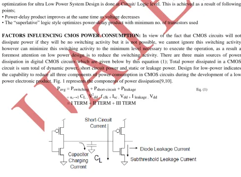
FACTORS INFLUENCING CMOS POWER CONSUMPTION: In view of the fact that CMOS circuits will not dissipate power if they will be no switching activity but it is not possible, we cannot ignore this switching activity however can minimize this switching activity to the minimum level necessary to execute the operation, as a result a foremost attention on low power design is to reduce the switching activity. There are three main sources of power dissipation in digital CMOS circuits which are given below by this equation (1); Total power dissipated in a CMOS circuit is sum total of dynamic power, short circuit power and static or leakage power. Design for low-power indicates the capability to reduce all three components of power consumption in CMOS circuits during the development of a low power electronic product. Fig. 1 represents the components of power dissipation[9,10].
Pavg = Pswitching + Pshort-circuit + Pleakage Eq. (1)
= αₒ→1 CL . V2dd . f clk + Isc . Vdd + I leakage . Vdd
= I TERM + II TERM + III TERM
5 |
P a g e
I TERM represents the switching component of power where αₒ→1 is the node transition activity factor; the average
number of times the node makes a power consuming transition in one clock period, CL is the load capacitance andfclk is
the clock frequency.
II TERM is resultant of direct path short circuit current Isc which is due to when both NMOS and PMOS transistors are
active at the same time, conducting current directly from supply to ground.
III TERM leakage current is consideration of fabrication process which is due to substrate injection and sub- threshold effects.
These all are responsible for power consumption in CMOS logic style and should be minimize. Power minimization can be done by use of GDI logic style at the place of CMOS design.
CONTRIBUTION OF DIFFERENT POWER DISSIPATION TERMS: As given by equation (1) Pswitching , P
short-circuit and Pleakage contributes to total power dissipation. Fig 2 shows contribution of these power dissipation terms
which gives switching power dissipation between 80 to 90%, leakage power dissipation between 10 to 30% and short circuit power dissipation between 0 to 05%. It is clear from this fig 1 that largest component of power dissipation comes from switching power, so with appropriate selection of logic style we will try to reduce this power dissipation. Fig 3 shows how static and dynamic powers related with the technology nodes. Scaling of technology node increases power-density more than predicted. CMOS technology beyond 65nm node presents an actual challenge for voltage and frequency scaling preliminary from 120nm node, every innovative procedure has inherently higher dynamic and leakage current density with minimum enhancement in speed. Among 90nm to 65nm the dynamic power dissipation is roughly same whereas there is ~5% higher leakage/mm2.Low cost forever continues to drive higher levels of integration, whereas low cost technological breakthroughs to maintain power under control are being paid very limited[4,5].
Fig 2: Contribution of different powers [1] Fig 3: Static and dynamic power vs transistor size [ ]
1.3 IMPORTANCE OF LOGIC STYLE FOR ULTRA LOW POWER DESIGN:
6 |
P a g e
characteristics of different existing logic styles can be compared with GDI and Mod-GDI logic style which reveals that this GDI and Mod-GDI logic style reducing power consumption and increasing speed of circuits[4,5].1.3.1 Impression of Logic Style: The logic style used in designing of basic logic gates and digital circuits is especially significant because this basically influences the speed, size, power dissipation, and the wiring complexity of a circuit. The speed, size, power dissipation, and the wiring complexity of a circuit is related to the circuit parameters as given below;
CIRCUIT DELAY: The delay of any circuit is calculated as a result of the number of inversion levels, the number of transistors in series, transistor sizes (i.e., channel widths), and intra- and inter-cell wiring capacitances.
CIRCUIT SIZE: The size of any circuit is greatly depends on the number of transistors used and their sizes and on the wiring complexity.
POWER DISSIPATION: Power dissipation of any circuit is determined by the switching activity and the node capacitances which results from gate, diffusion, and wire capacitances.
WIRING COMPLEXITY: The wiring complexity of any circuit is measure of connections made on the circuit. The wiring complexity can determine by the number of connections and the lengths of connections and by whether single-rail or dual-rail logic is used.
All above said characteristics of ant circuit possibly will be different significantly from one logic style to another logic style used for designing. Though formulate the appropriate selection of logic style fundamental for circuit performance on low power and high speed. At the same time as far as cell-based design techniques (e.g., standard-cells like GDI cell, Mod-GDI cell) and logic style are concerned, user-friendliness and simplification of logic functions is of significance as well. There are other important aspects which are influenced by the use of logic style for designing and these are Robustness and surrounding environments. Robustness with respect to voltage and transistor scaling, robustness with respect to the changeable development and functioning circumstances are important. On the other hand compatibilitywith surrounding circuitries is also very crucial point.
1.3.2 Necessities of Low Power Logic Style: Dynamic power dissipation of a digital CMOS circuit is given by this equation (2)
Pd=Vdd2.fclk.Ʃn αn.Cn + Vdd. Ʃn iscn . Eq,(2)
According to the equation (2) the dynamic power dissipation of a digital CMOS circuit depends on the followings: The supply voltage: Vdd
The clock frequency: fclk
The node switching activities: αn The node capacitances: Cn The node short-circuit currents: iscn And the number of nodes n.
A reduction in dissipated power can be achieved by means of reduction in each of these parameters which are responsible for power dissipation. The clock frequency: fclk reduction cannot be done at any level of design, it is only achievable at the architecture level, while at the circuit level ;clock frequency fclk is generally taken as constant in order to accomplish some specified throughput requirement. All the other parameters of equation (2) are influenced to a little extent by the use of logic style. Therefore, some general logic style which fulfills the requirements for low-power circuit implementation can be established at this point.
7 |
P a g e
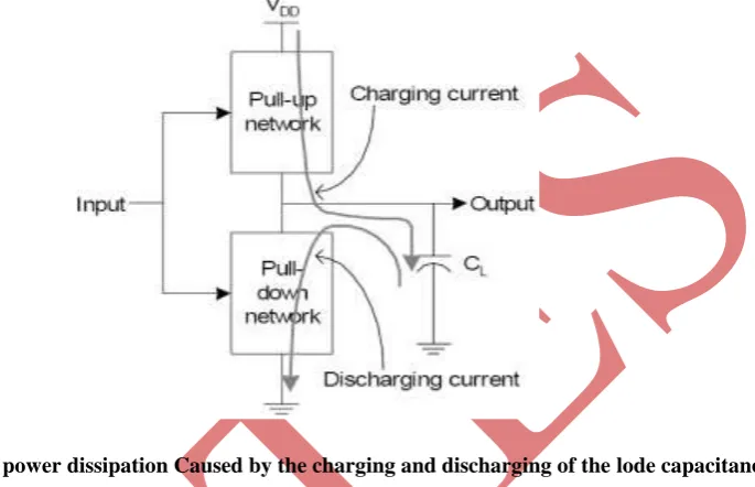
transistors as possible and circuit nodes as possible, and by sinking transistor sizes to a minimum sizes. As the switching capacitance also depends on interconnections of circuits, the number of high capacitive, inter-cell connections and length of these connections which is influenced by the circuit size be supposed to be kept at smallest. An additional basis for capacitance reduction is established at the layout level, which, on the other hand, is not considered here. Transistor size scaling such that transistor downsizing is an efficient method to reduce switched capacitance of logic gates. On behalf of that transistor downsizing, a logic style should be vigorous against transistor downsizing, i.e., accurate performance of logic gates with minimum or near-minimum transistor sizes are required to be definite.Fig 4: Switching power dissipation Caused by the charging and discharging of the lode capacitance
2) Supply voltage reduction: One familiar method for reducing power is power supply scaling. For CMOS circuits the cost of lower supply voltage is lower performance. Supply voltage reduction offers the most efficient way of minimizing power consumption. Supply voltage reduction does not requires any extraordinary circuits or technologies, in spite of this a factor of two reductions in supply voltage results a factor of four decreases in power consumption. That‟s why; this power reduction method is a universal outcome, practiced not only in one sub-circuit or block of the chip, but all over the entire design. For the basis of these factors, manufacturers are frequently keen to sacrifice increased physical capacitance or circuit activity for Supply voltage reduction. Unluckily, there is also paying of a speed penalty for supply voltage reduction, because delays significantly increasing as Vddapproach the threshold voltage Vt of the devices which results in limit the functional range of Vddto a minimum of about 2-3 Vt.
The supply voltage and the selection of logic style are ultimately correlated through delay-driven voltage scaling. That is, a logic style presenting fast logic gates to speed up vital signal paths allows a reduction of the supply voltage in order to accomplish a given throughput. For all these reasons, a logic style is required to be robust against supply voltage reduction, which means, performance and accurate operation of logic gates have to be definite at low voltages as well. This becomes a serious difficulty at very low voltages of about 1 V and lower, somewhere noise margins become critical.
8 |
P a g e
Switching activity of any circuits is in addition a function of the logic style used to implement the circuit. The functional activity in dynamic circuits is forever superior to that in static implementation of the same circuit since all nodes are pre-charged to some value such that 1 in N-type dynamic and 0 in P-type dynamic, previous to the fresh input data arrives. This process efficiently increases the number of power consuming transitions. Remind that the physical capacitance in dynamic logic tends to be less important than that in static logic; as a result the alternative between dynamic and static logic implementations is not at the same time as clear as it would be otherwise in addition Dynamic circuits are as well glitch-free.Estimation of Switching Activity
: computation of the switching activity in a logic circuit is complicated because it
depends on a number of circuit parameters and technology-dependent factors which are not willingly accessible or accurately characterized. A number of these factors are ; Input Pattern Dependence, Delay Model, Logic Function, Logic Style, Circuit Structure, and Statistical Variation of Circuit Parameters.4) Short-circuit current reduction: Short-circuit currents or dynamic leakage currents possibly will fluctuate with a significant quantity among different logic styles used for the circuit designing. They also strongly depend on input signal slopes, Load, The transistor size of the gate, Supply voltage, Frequency and Threshold voltage. The Short-circuit currents contribution to the overall power consumption is somewhat limited but still not insignificant (≈10–30%), with the exception for very low voltage levels such that Vdd ≤ Vtn +│Vtp│, where the short-circuit currents vanishes. A low-power logic style be supposed to include minimum short-circuit currents and, of course, no static currents as well the inbuilt CMOS leakage currents.
1.3.3 Logic Style Requirements for user-friendliness: A selected logic style is supposed to be extremely robust and included pleasant electrical characteristics for user-friendliness and generality of gates. So like to this is decoupling of gate inputs and outputs which means at least one inverter stage per gate as well as good driving capabilities and full signal swings at the gate outputs, to facilitate logic gates work consistently in any circuit configuration. These characteristics are fundamentals for cell-based design and logic styles. Additionally, a logic style is supposed to allow the competent implementation of arbitrary logic functions and make available little regularity with respect to circuit and layout realization. Jointly low-power and high-speed versions of logic cells should be supported in order to allow flexible power-delay tuning by the designer or the synthesis tool.
Gate diffusion input is a new technique of low-power digital circuit design described in this paper. This technique allows reducing power consumption, propagation delay, and area of digital circuits while maintaining low complexity of logic design. The object of this research is to develop a faster, lower power, and reduced area alternative to standard CMOS logic circuits. This research has resulted in the development of many logic design techniques during the last two decades. One popular alternative to CMOS is GDI logic style. The GDI approach allows implement of a wide range of complex logic functions using only two transistors[5].
II.GATE DIFFUSION INPUT LOGIC STYLE (GDI)
9 |
P a g e
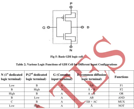
Fig 5: Basis GDI logic cell
Table 2; Various Logic Functions of GDI Cell for Different Input Configurations
N (1
stdedicated
logic terminal)
P(2
nddedicated
logic terminal)
G (Common
input terminal)
D (common diffusion
logic terminal)
Functions
Low B A ĀB F1
B High A Ā + B F2
High B A A + B OR
B Low A AB AND
C B A ĀB + AC MUX
Low High A Ā NOT
2.1KEY FUNCTIONS OF GDI LOCIC CELL:
The GDI logic style approach allows implementation of broad range of multifaceted functions using only two transistors. This method is for this reason appropriate for design of high-speed and low-power circuits using reduced number of transistors compared to CMOS and existing PTL logic techniques. The GDI logic style method uses a simple basic GDI cell which looks closely similar to the basic CMOS inverter at first glimpse and reminds one of the standard CMOS inverter, except present various remarkable differences which are listed below.
1. The basic GDI cell contains 3 inputs: G (common gate input of nMOS and pMOS), P (input to source of pMOS), and N (input to source of nMOS) while there are not three inputs in CMOS inverter circuit.
2. Bulks of both nMOS and pMOS are connected to N or P respectively so with the purpose of can be arbitrarily biased which is in contrast with a CMOS inverter.
3. The basic GDI cell allows implementation of logic functions using only two transistors which is not possible with CMOS inverter.
We can realize all basic logic gates and universal gates also with this GDI cell; we can conclude that the GDI logic style approach consumes less silicon area compared to other logic styles. In view of the fact that, the area is less, the value of node capacitances will be less and for this reason GDI gates have faster operation which presents that GDI logic style is a power efficient method of design.
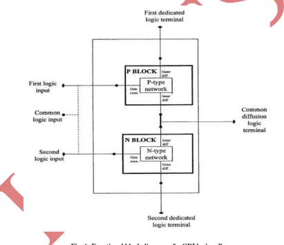
2.2FUNCTIONAL BLOCK DIAGRAM OF GDI LOGIC CELL:
10 |
P a g e
second dedicated logic terminals and the common diffusion logic terminal are capable of every work as either a logic signal input terminal or a logic signal output terminal, depending upon the precise logic circuit implementation [1,2].The P logic block contains arrangement of p-type transistors that are interconnected for the purpose of implement a given logic function. The P logic block has three logic connections that are as follows; one is an outer diffusion connection which is at an outer diffusion node of one of the p-type transistors, the second is a gate connection which is at the gate of one of the p-type transistors, and the third is an inner diffusion connection which is at the second inner diffusion node of one of the p-type transistors. Outer diffusion connection connects to the first dedicated logic terminal, and gate terminal connects to the first logic input.
The N logic block contains arrangement of n-type transistors, which implement the complementary logic function, and is prepared likewise to the P logic block.
Common diffusion logic terminal; In the Common diffusion logic terminal the inner diffusion nodes of the P and N logic blocks are connected mutually to form the common diffusion logic terminal.
Common logic input; the common logic terminals are connected mutually to form a common logic input. Consequently a logic signal at the common logic input is applied to both the P and N logic blocks.
Fig. 6: Functional block diagram of a GDI logic cell
11 |
P a g e
Therefore, for GDI logic style one of the two transistor diffusion nodes only not the gate is randomly selected to work for the inner diffusion connection, and the other to work for the outer diffusion connection. Numerous GDI cell topologies are able to be implemented in standard p-well or n-well CMOS technology, due to interference of bulk effects under definite input/output circumstances, GDI logic style are consequently preferably implemented in either twin-well CMOS or silicon-on-insulator (SOI) or silicon-on-sapphire (SOS) technologies, which do not experiences these limitations.2.3 GDI CIRCUITS HAVING SOME PRACTICAL LIMITATIONS
a.GDI circuits also faces problem of swing degradation like PTL circuit design. For eliminating this problem of swing degradation, a method is used for swing restoration in which a buffer stage is used after every GDI cell, presented by Fish et.al [1]. But this is not a good quality solution because adding buffer after every logic cell will lead to increased area and reduced delay. the problem of threshold drop is not a very serious issue when we go in sub nm regions.
b.The most important complexity that GDI logic style faces is difficulty in fabricate in standard CMOS process.
c.If twin-well process is used for implementation, the cell area is increased area due to the need for separate wells for each transistor. Fish et.al [2] has proposed a modified version of their GDI cell to make it standard CMOS process compatible.
d.The bulks of nMOS and pMOS are constantly connected to VDD and GND respectively.
III.MODIFIED GATE DIFFUSION INPUT LOGIC STYLE (Mod-GDI)
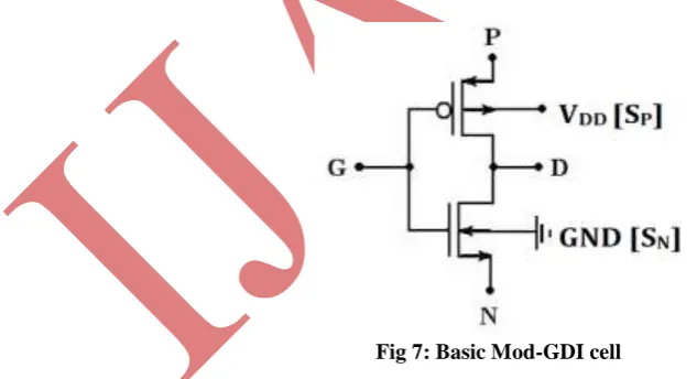
Power dissipation becomes most important restriction in high performance applications. Optimizations for basic logic gates are fundamental in order to get better the performance of a variety of low power and high performance devices. These limitations can be overcome by modified gate diffusion input (Mod-GDI) logic style[4,5]. This technique allows reducing power consumption, delay and area of digital circuits. Fig 7 shows basic Mod-GDI logic style. In contrast with the basic GDI cell, Modified-GDI [Mod-GDI] cell contains a low-voltage terminal SP configured to be connected to a high constant voltage (i.e. supply voltage) and a high-voltage terminal SN configured to be connected to a low constant voltage (i.e. Ground). Including terminals these ensures that the Mod-GDI cell can be implemented with all current CMOS technologies.
Fig 7: Basic Mod-GDI cell
12 |
P a g e
capable of as well implemented in all kinds of non-standard technologies, like twin-well CMOS technology, Silicon on Insulator (SOI) technology and Silicon on Sapphire (SOS) technology[8].3.1ADVANTAGES OF MOD-GDI:
This straightforward arrangement as shown in Fig 7 has made the fabrication of GDI cells compatible with the
standard nano-scale CMOS fabrication process. Whereas many leakage components can be recognized in sophisticated sub-micron technologies, the most important leakage currents are given below[1,2,3]:1. Sub-Threshold Leakage
2. Gate Leakage (caused by electron tunneling)
This exceptional arrangement of Mod-GDI cell provides considerable reduction of both sub-threshold and gate leakage compared to static CMOS gate.
These methodologies may be used as a basis for efficient synthesizer implementation, to achieve area efficient designs such as; Reduction Of Short-Circuit Current, Repeaters etc.
Table 3 presents the various logic functions which can be implemented with the help of MOD-GDI cell for different input configurations.
Table 3: Various Logic Functions of Mod-GDI Cell for Different Input Configurations
N SN P SP G D FUNCTIONS
O 0 1 1 A A‟ INVERTER
A A 0 A B AB AND
1 0 A D B A+B OR
A‟ 0 A 1 B A‟B+AB‟ XOR
A 0 A‟ 1 B AB+A‟B‟ XNOR
0 0 B B A A‟B FUNCTION 1
B 0 1 1 A A‟+B FUNCTION 2
C 0 B 1 A A‟B+AC MUX
3.2IMPORTANT FEATURES OF M-GDI TECHNIQUE IN BREIF:
a. The Mod-GDI logic style provides a low-power and area efficient substitute to existing logic styles, which is implementable in all current CMOS transistor fabrication technologies. Mod-GDI is appropriate for design of high-speed, low power circuits, using reduced number of transistors, even as improving swing degradation and static power characteristics, and allowing easy top-down design by using a small cell library. Mod-GDI is appropriate for implementation of a broad range of logic circuits, using a variety of transistor technologies. Mod-GDI logic style performance is testable; so that Mod-GDI logic style and logic circuit design methods is therefore a promising new approach to logic circuit design.
b. Realization of logic functions in Silicon-on-Insulator (SOI) or Silicon-on-Sapphire (SOS) fabrication technologies presents considerable reduction of wires used for interconnect, in these methods, the floating bulk transistors are frequently used for logical circuit‟s implementations for GDI logic style and for other existing logic styles. Floating bulk transistors not requires connections of the VDD and GND wires to the transistors bulks. Consequently, when a logic function is implemented with Mod-GDI cells with SOI or SOS transistors, VDD and GND interconnect wires are not required because the Mod-GDI cell requires VDD and GND only to supply the bulks. This is in contrast to the majority previous design methodologies which would still need VDD and GND to supply the circuits.
IV.DC & TRANSIENT ANALYSIS OF FUNCTIONS USING MODIFIED GDI TECHNIQUE
13 |
P a g e
an analysis is done and all logic functions are verified with the help of DC and Transient analysis. Based on the results power delay is calculated for Mod-GDI logic style and compared with the CMOS logic style, which shows that Mod-GDIlogic style is more beneficial for lower power digital design
.
1.
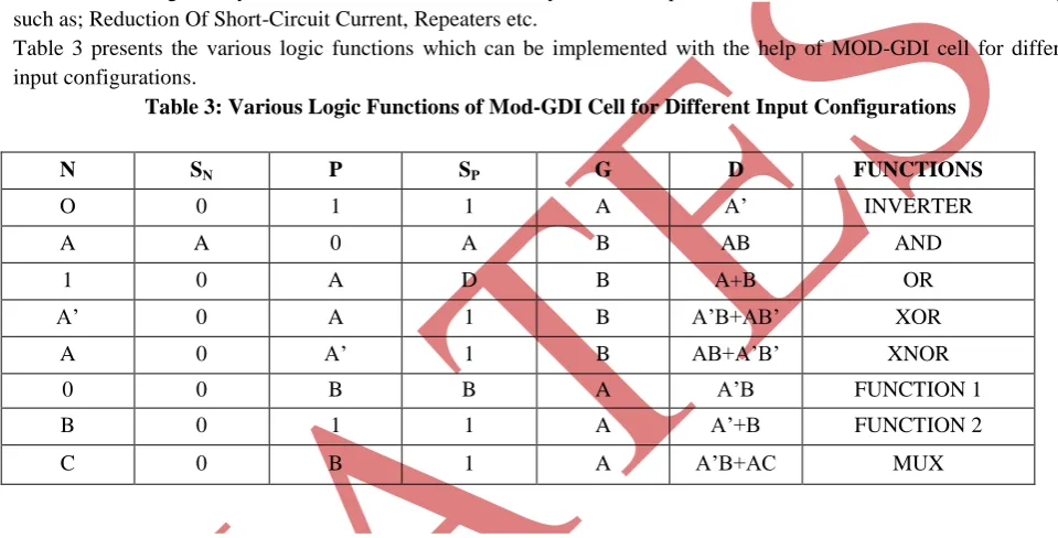
IMPLEMENTATION OF Mod-GDI ‘OR’ FUNCTION
When input G = A, P = B, SP = D, N = VDD [1 or High], and SN = 0, then output D = A+B which is OR function. Fig 8 shows input configuration for Mod-GDI OR Fn, where;
Fig 8: M-GDI ‘OR’ Fn
At Node „1‟ input G = A is given, At Node „2‟ input P = B is given, At Node „3‟output D = A+B is taken,
At Node „4‟ input N = VDD [1 or High] is given.
i)
DC ANALYSIS; Truth Table:
Input output
G = A P = B SP N=VDD=1 SN D = A+B; [ OR Fn]
0 [ 0V] 0 [ 0V] D 1 0 0 [0.000005 V]
0 [ 0V] 1 [ 5V] D 1 0 1 [ 4.99 V]
1 [ 5V] 0 [ 0V] D 1 0 1 [ 3.55 V]
1 [ 5V] 1 [ 5V] D 1 0 1 [ 3.55 V]
ii)
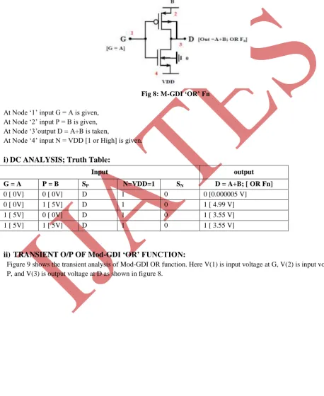
TRANSIENT O/P OF Mod-GDI ‘OR’ FUNCTION:
14 |
P a g e
T i m e0 s 2 0 n s 4 0 n s 6 0 n s 8 0 n s 1 0 0 n s
V ( 1 ) V ( 2 ) V ( 3 ) 0 V
2 . 0 V 4 . 0 V 6 . 0 V
Fig 9: M-GDI ‘OR’ Fn Transient Response
2.
IMPLEMENTATION OF Mod-GDI ‘AND’ FUNCTION
When input G = A, N = B, P = 0, SP = VDD [1 or High], and SN = 0, then output D = A.B which is AND function. Fig 10 shows input configuration for Mod-GDI AND Fn, where ;
Fig 10: Mod-GDI ‘AND’ Fn
At Node „1‟ input G = A is given, At Node „2‟ input N = B is given, At Node „3‟output D = A.B is taken, At Node „4‟ input P = 0 is given.
i)
DC ANALYSIS; Truth Table:
Input output
G = A N = B SN P=0 SP D = AB; [ AND Fn]
0 [ 0V] 0 [ 0V] 0 0 VDD 0 [0.000005 V]
0 [ 0V] 1 [ 5V] 0 0 VDD 0 [0.000005 V]
15 |
P a g e
1 [ 5V] 1 [ 5V] 0 0 VDD 1 [ 3.552 V]
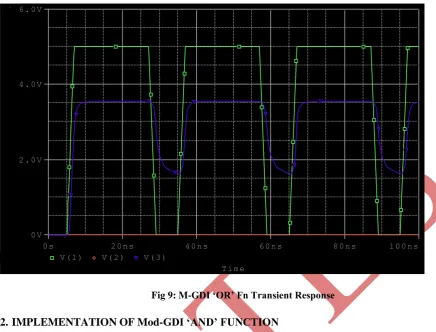
ii)TRANSIENT O/P OF Mod-GDI ‘AND’ FUNCTION:
Figure 11 shows the transient analysis of Mod-GDI AND function. Here V(1) is input voltage at G, V(2) is input voltage at N, and V(3) is output voltage at D as shown in figure 10.
T i m e
0 s 2 0 n s 4 0 n s 6 0 n s 8 0 n s 1 0 0 n s
V ( 1 ) V ( 2 ) V ( 3 ) 0 V
2 . 0 V 4 . 0 V 6 . 0 V
Fig 11: Mod-GDI ‘AND’ Fn Transient Response
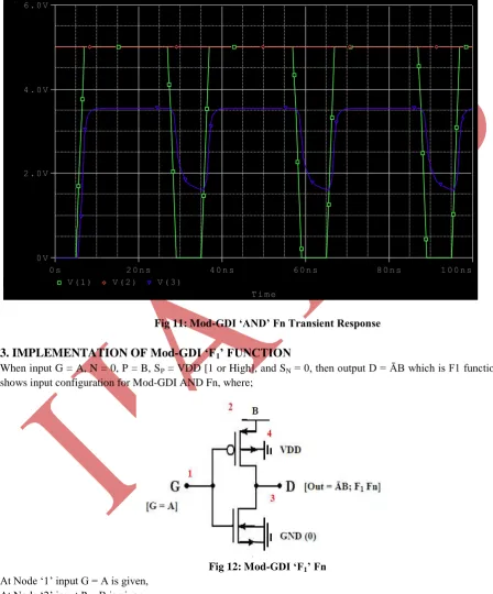
3. IMPLEMENTATION OF Mod-GDI ‘F1’ FUNCTION
When input G = A, N = 0, P = B, SP = VDD [1 or High], and SN = 0, then output D = ᾹB which is F1 function. Fig 12 shows input configuration for Mod-GDI AND Fn, where;
Fig 12: Mod-GDI ‘F1’ Fn
16 |
P a g e
i)
DC ANALYSIS; Truth Table:
Input output
G = A P = B SP N= 0 SN D = ᾹB; [ F1 Fn]
0 [ 0V] 0 [ 0V] VDD 0 0 0 [0.000005 V]
0 [ 0V] 1 [ 5V] VDD 0 0 1 [4.99 V]
1 [ 5V] 0 [ 0V] VDD 0 0 0 [0.000000002 V]
1 [ 5V] 1 [ 5V] VDD 0 0 0 [0.000000002 V]
ii)TRANSIENT O/P OF Mod-GDI ‘F1’ FUNCTION:
Figure 13 shows the transient analysis of Mod-GDI F1 function. Here V(1) is input voltage at G, V(2) is input voltage at P, and V(3) is output voltage at D as shown in figure 12.
T i m e
0 s 2 0 n s 4 0 n s 6 0 n s 8 0 n s 1 0 0 n s
V ( 1 ) V ( 2 ) V ( 3 )
- 2 . 0 V 0 V 2 . 0 V 4 . 0 V 6 . 0 V
Fig 13: Mod-GDI ‘F1’ Fn Transient Response
4. IMPLEMENTATION OF Mod-GDI ‘F2’ FUNCTION
When input G = A, N = B, P = 1, SP = VDD [1 or High], and SN = 0, then output D = Ᾱ+B which is F2 function. Fig 14 shows input configuration for Mod-GDI F2 Fn, where
Fig 14: Mod-GDI ‘F2’ Fn
17 |
P a g e
At Node „2‟ input N = B is given,At Node „3‟output D = Ᾱ+B is taken, At Node „4‟ input P = 1 is given.
i)
DC ANALYSIS; Truth Table:
Input output
G = A N = B SN P= 0 SP D = Ᾱ+B; [ F2 Fn]
0 [ 0V] 0 [ 0V] 0 1 1 1 [4.99 V]
0 [ 0V] 1 [ 5V] 0 1 1 1 [4.99 V]
1 [ 5V] 0 [ 0V] 0 1 1 0 [0.000000002 V]
1 [ 5V] 1 [ 5V] 0 1 1 0 [ 3.55 V]
ii)TRANSIENT O/P OF Mod-GDI ‘F2’ FUNCTION:
Figure 15 shows the transient analysis of Mod-GDI F1 function. Here V(1) is input voltage at G, V(2) is input voltage at N, and V(3) is output voltage at D as shown in figure 14.
T i m e
0 s 2 0 n s 4 0 n s 6 0 n s 8 0 n s 1 0 0 n s V ( 1 ) V ( 2 ) V ( 3 )
- 2 . 0 V 0 V 2 . 0 V 4 . 0 V 6 . 0 V
Fig 15: Mod-GDI ‘F2’ Fn Transient Response
5. IMPLEMENTATION OF Mod-GDI ‘MUX’ FUNCTION
18 |
P a g e
Fig 16: Mod-GDI ‘MUX’ Fn
At Node „1‟ input G = A is given, At Node „2‟ input P = B is given, At Node „3‟output N = C is given, At Node „4‟ input SP = VDD is given. At Node „5‟ output D = ᾹB+ AC is taken.
i)
DC ANALYSIS;Truth Table:
Input output
G = A P = B SP N= C SN D = ᾹB+ AC; [ MUX Fn]
0 [ 0V] 0 [ 0V] VDD 0 [ 0V] 0 0 [0.000005 V]
0 [ 0V] 0 [ 0V] VDD 1 [ 5V] 0 0 [0.000005 V]
0 [ 0V] 1 [ 5V] VDD 0 [ 0V] 0 1 [ 4.99 V]
0 [ 0V] 1 [ 5V] VDD 1 [ 5V] 0 1 [ 4.99 V]
1 [ 5V] 0 [ 0V] VDD 0 [ 0V] 0 0 [0.000000002 V]
1 [ 5V] 0 [ 0V] VDD 1 [ 5V] 0 1 [ 3.552 V]
1 [ 5V] 1 [ 5V] VDD 0 [ 0V] 0 0 [0.000000002 V]
1 [ 5V] 1 [ 5V] VDD 1 [ 5V] 0 1 [ 3.552 V]
ii)TRANSIENT O/P OF Mod-GDI ‘MUX’ FUNCTION:
19 |
P a g e
T i m e0 s 2 0 n s 4 0 n s 6 0 n s 8 0 n s 1 0 0 n s V ( 1 ) V ( 2 ) V ( 3 ) V ( 5 )
- 2 . 0 V 0 V 2 . 0 V 4 . 0 V 6 . 0 V
Fig 17: Mod-GDI ‘MUX’ Fn Transient Response
6. IMPLEMENTATION OF Mod-GDI ‘Inverter’ FUNCTION
When input G = A, N = 0, P = 1, SP = VDD [1 or High], and SN = 0, then output D = Ᾱ which is INVERTER function. Fig 18 shows input configuration for Mod-GDI INVERTER Fn, where
At Node „1‟ input G = A is given, At Node „2‟ input P = 1 is given, At Node „3‟ output D = Ᾱ is taken.
Fig 18: Mod-GDI ‘Inverter’ Fn
i)
DC ANALYSIS; Truth Table:
Input output
G = A P = 1 SP N= 0 SN D = Ᾱ; [ Inverter Fn]
0 [ 0V] 1 1 0 0 1
20 |
P a g e
ii)TRANSIENT O/P OF Mod-GDI ‘INVERTER’ FUNCTION:
Figure 19 shows the transient analysis of Mod-GDI INVERTER function. Here V(1) is input voltage at G and V(3) is output voltage at D as shown in figure 18.
T i m e
0 s 2 0 n s 4 0 n s 6 0 n s 8 0 n s 1 0 0 n s V ( 1 ) V ( 3 )
- 2 . 0 V 0 V 2 . 0 V 4 . 0 V 6 . 0 V
Fig 19: Mod-GDI ‘INVERTER’ Fn Transient Response
V. COMPARISION OF DELAY & POWER OF LOGIC FUNCTIONS IN Mod-GDI AND CMOS
LOGIC
The performance analysis of Mod-GDI and CMOS logic is presented in this table 4. The performance evaluation is made with respect to the switching delay, transistor count and power consumed by Mod-GDI and CMOS logic. From the analysis it is observed that the Mod-GDI performance is better when comparing to CMOS logic. In CMOS the number of transistors used to realize a function is twice that of Mod-GDI. The power consumed by CMOS is slightly higher than Mod-GDI.
Table 4; comparison of delay & power of logic functions in MOD-GDI and CMOS logic
Function
Logic
Expression
MOD-GDI LOGIC
CMOS LOGIC
Power
(µw)
Delay
(ns)
No.of
Transistors
Power
(µw)
Delay
(ns)
No.of
Transistors
OR A+B 17.8 1.01 2 25.0 1.77 6
AND A.B 17.9 1.10 2 25.0 1.54 6
21 |
P a g e
F2 Ᾱ+B 25.0 0.40 2 42.72 1.70 8
MUX ᾹB+AC 25.0 0.50 2 54.64 1.69 12
Table 4 and 5 shows that GDI logic style as well as Mod-GDI logic style both are superior than CMOS logic style for low power design as the no. of transistors used for implementing basic logic gates are less than that are used in CMOS logic design.
Table5; Comparison of Basic logic gates in GDI and CMOS logic design
GDI BASED GATES
CMOS BASED GATES
X
O
R
G
A
T
E
4transistors used
12 transistors used
A
N
D
G
A
T
E
2 transistors used
6 transistors used
O
R
G
A
T
22 |
P a g e
2 transistors used
6 transistors used
CONCLUSION
In this paper an approach is presented for minimizing power consumption for digital circuits at the logic style level and DC and Transient analysis of basic logic gates has been done using Mod-GDI logic style. All Simulations are performed through PSPICE based on 0.18μm CMOS technology, and results show power characteristics of Mod-GDI technique of low power digital circuit design. Simulation results shows up to 45% reduction in power-delay product in Mod-GDI. Mod-GDI approach allows realization of a broad variety of multifaceted logic functions by means of only two transistors. Mod-GDI gates lower the transistor count and in turn the silicon area required when compared to standard static CMOS and Domino CMOS based approaches. The leakage power and switching power of Mod-GDI gates is lower than the traditional logic styles. The problem of fabrication of GDI gates in standard nano-scale CMOS process is overcome by connecting the sources of pMOS and nMOS to VDD and GND respectively in Mod-GDI logic style. The problem of threshold drop is not a very serious issue in deep sub-nm regions.
The Mod-GDI logic style based design adopts interruption of inverter to alleviate the problem of signal degradation during propagation. This proposed logic style is analyzed to exploit the high speed potential and low power feature of Mod-GDI based circuit applications. The comparison between our analysis and prior works indicates that one of this logic styles for low power digital design does provide many advantages. In short, the proposed Mod-GDI logic style based designs can be taken a better alternative in future.
For the period of the desktop PC design and portable age VLSI design efforts have paying attention primarily on optimizing speed to realize computationally intensive real-time functions such as video compression, gaming, graphics etc. As a result, semiconductor ICs that successfully integrated a variety of complexes signal processing modules and graphical processing units to meet up computation and entertainment demands. As these solutions have addressed the real-time problem, they have not addressed the increasing demand for portable operation, where mobile phone needs to pack all this without consuming much power. The severe limitation on power dissipation in portable electronics applications such as smart phones and tablet computers must be met by the VLSI chip designer while still meeting the computational requirements. At the same time as wireless devices are quickly making their way to the consumer electronics market, a key design restriction for portable operation that is the total power consumption of the device must be taken into account. So for this purpose reducing the total power consumption in such systems is significant because it is advantageous to maximize the run time with minimum requirements on size, battery life and weight allocated to batteries. Consequently the most significant issue to consider while designing portable devices is 'low power design' for which a Mod-GDI logic style is proposed.
![Fig 2: Contribution of different powers [1] Fig 3: Static and dynamic power vs transistor size [ ]](https://thumb-us.123doks.com/thumbv2/123dok_us/9164395.1454850/5.595.51.533.228.590/fig-contribution-different-powers-static-dynamic-power-transistor.webp)