A Generic Framework for Rapid Prototyping of System-on-Chip
Designs
Dmitrij Kissler, Alexey Kupriyanov, Frank Hannig,
Dirk Koch, J¨urgen Teich
Department of Computer Science 12,
Hardware-Software-Co-Design,
University of Erlangen-Nuremberg, Germany.
Abstract
The integration of different Intellectual Property (IP) cores to modern System-on-Chip (SoC) designs be-comes more and more an important topic because of the benefits in the overall system performance and the design costs. In this paper we present a new generic framework consisting of a graphical user interface with an extendable highly parameterizable IP component li-brary for convenient SoC architecture entry, as well as software tools, which provide an automatic generation of fast cycle-accurate simulators for verification pur-poses and synthesizable HDL code for hardware syn-thesis. Because the communication of the single IP cores also plays an important role, our IP core library includes an open-source bus component, which is used in a case study design.
1
Introduction
The integration of several functional IP cores into a sin-gle SoC is advantageous because of the better perfor-mance characteristics, lower power consumption, lower production costs as well as a higher degree of minia-turization than in the case of separated units. These are the key properties needed in such fast growing ar-eas of application as mobile communication, multi-media, and portable entertainment devices. A typi-cal SoC design usually consists of one or more inte-grated processor cores, embedded memory, a number of dedicated hardware components, input/output mod-ules and finally it contains an On-Chip-Bus (OCB) for communication purposes. As target technology ASICs (Application-Specific Integrated Circuit) as well as Field-Programmable Gate Arrays (FPGA) are de-ployed. The importance of SoC is apparent in consider-ation of the fact, that leading FPGA manufacturers such as Altera and Xilinx brought their own systems on the market: from Altera the EXCALIBURsystem with the
NIOS or ARM processor and from Xilinx the hard IP core of the POWERPC or alternatively the soft IP core of the MICROBLAZEprocessor for the FPGAs.
2
Related Work
Several software tools are available for the specification of SoC designs [1–5]. The system-on-a-programmable-chip builder (SOPC Builder) [6] from Altera is such a tool, which allows the user to define SoC designs graphically and automatically generate VHDL or Ver-ilog source code according to this description. The SoCLib project [7] is an open modeling and simula-tion platform for multiprocessor SoC. The core of the project is a library of simulation models for several IP cores, written in SystemC. Two abstraction levels are available: cycle-accurate/bit-accurate and TLM (trans-action level modeling). However, the synthesizable models for these IP cores are not available due to legal restrictions. All of the SoCLib components implement the VCI [8] protocol. The simulation of the generated HDL code is not integrated into these tools and has to be done with external simulation software, like Model-sim [9].
Modules for the interconnection of single IP cores to a complete System-on-Chip play a very important role. The choice of the right interconnect architecture has a strong effect on the system performance [10], development time and consequently project costs. At the beginning of SoC development proprietary inter-connection schemes which were not compatible to each other were utilized. As the system complexity increased the need for standardized bus interconnection schemes grew and different commercial as well as open-source standards were developed. The best known commer-cial systems include the CORECONNECTbus architec-ture from IBM [11], the AMBAbus from Arm Ltd. [12], and the AVALONbus from Altera [13]. As a
represen-tative for an open-source bus system one can name the WISHBONEbus originally designed by Silicore Corpo-ration [14]. One difficulty with the different On-Chip-Buses (OCBs) is, that the interface to the specific OCB is usually integrated into the functional logic of the IP core components. Therefore, they must first be adapted to some other OCB. This cannot always be done eas-ily, especially if only hard or firm IP cores are avail-able. The SOPC Builder and the SoCLib library, respec-tively, integrate the interface to the specific OCB into the functional logic of the components and these CAD tools provide only IP cores with this specific bus inter-faces. To deal with this problem one could implement the core-centric protocol OCP-IP (Open Core Protocol International Partnership) [15] which introduce de facto a new bus protocol as an abstraction layer over the ex-isting OCBs. To keep the possibility to integrate new IP cores regardless which OCB interface they implement, we use another approach, namely to separate the actual bus interface from the application specific logic of the IP core. This results in master and slave modules which are connected with the functional IP cores. With this technique it is possible to interconnect IP cores which are not provided with a special bus interface. Further-more, we use the WISHBONE bus and its concept of tag signals, which is explained in detail in our case study in Section 5.
The main contributions of this paper can be summa-rized as follows:
• A new integrated framework was built for graphi-cal, system-level modeling of reconfigurable SoC designs,
• Automatic generation of fast cycle-accurate simu-lators and generation of synthesizable HDL code was integrated into the framework,
• A separation is made between the functional logic of an IP core and its bus interface and no additional (abstract) bus protocols are needed.
The rest of the paper is structured as follows. In Section 3, we present our integrated SoC framework. Subsequently, in Section 4, our generic interconnect methodology is discussed. Our approach was tested in a case study, Section 5, with a MIPS processor and pe-ripheral devices on an Altera Cyclone FPGA. Finally, we conclude our paper in Section 6 with a summary and outlook.
3
System Integration Framework
ARCHITECTURECOMPOSERis a framework for graph-ical and interactive architecture entry and composition. Its origin is the BUILDABONG project [16], [17], a
project for architecture and compiler co-design of em-bedded application specific instruction set processors (ASIPs). In ARCHITECTURECOMPOSERthe designer chooses from a library of customizable building blocks to compose graphically his desired architecture. This is done by connecting instantiated components with each other. The library contains a lot of necessary modules for the processor design such as register files, memo-ries, multiplexers, arithmetic and logical units, simple busses, and others. All components are parametric, e.g. the word width of the modules can be chosen arbitrar-ily. Furthermore, ARCHITECTURECOMPOSERoffers a hierarchical architecture entry to handle complex sys-tems ant to reuse already designed subsyssys-tems. Realis-tic microprocessors such as a MIPS processor or a DSP from Texas Instruments TMS320C6 series have been successfully modeled within hours. From the graphical architecture description a mixed structural/behavioral model of the architecture is generated automatically. This model is based on the formalism of Abstract State Machines (ASM) [18]. Additionally, a debugging and simulation environment which allows to verify the func-tionality of the given architecture on pipeline-cycle and instruction-cycle levels is generated. At any time, the graphically entered hardware architecture can be au-tomatically transformed into a synthesizable hardware description language program. Three HDL-generators, namely, for VHDL, Verilog, and SystemC are avail-able. The aim to bring the ARCHITECTURECOMPOSER
framework to the higher level of System-on-Chip and multi-core interactive design required two things. First, faster simulations as the above described ASM ap-proach were needed thus we recently developed the so-called RasimSimulator [19], [20], which can automati-cally generate a stand-alone cycle-accurate and bit-true C++-compiled fast simulator which executes the sim-ulation approximately up to two orders of magnitude faster, compared to the Modelsim [9] VHDL-RTL sim-ulation. Second, the integration of Wishbone OCB and several peripheral IP as presented in this paper are nec-essary to bring the framework to the higher level of SoC design.
Before we present the case study in detail, we would like to give an overview over our interconnect method-ology of IP cores in the next section.
4
Interconnection Methodology
In the embedded system industry bus architectures for core interconnection became widely accepted. Since several bus standards exist, each manufacturer of an IP core tailors its product to the bus architecture of his choice. Abstractly speaking, the IP core manufacturer
HADDR HWRITE
HRDATA
HWDATA
DAT_I
DAT_O ADR_O WE_O DAT_I
HWDATA HRDATA HADDR
DAT_O ADR_I WE_I
HRESP HRESP
Wishbone Master Wishbone Slave
TGD_O
TGD_I ... ...
AMBA AHB Master AMBA AHB Slave
IP Core IP Core
Wishbone Interconnect
HWRITE
Figure 1: Tag signals treatment in Wishbone.
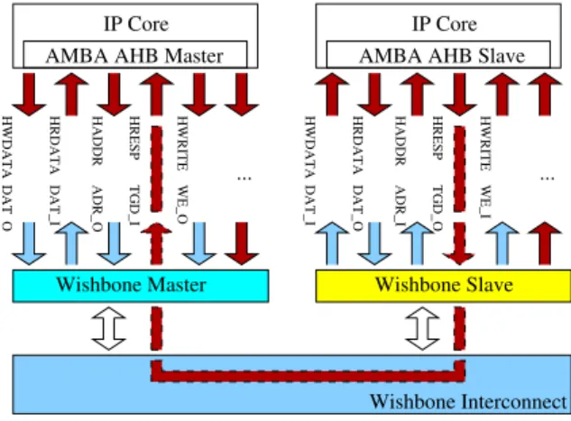
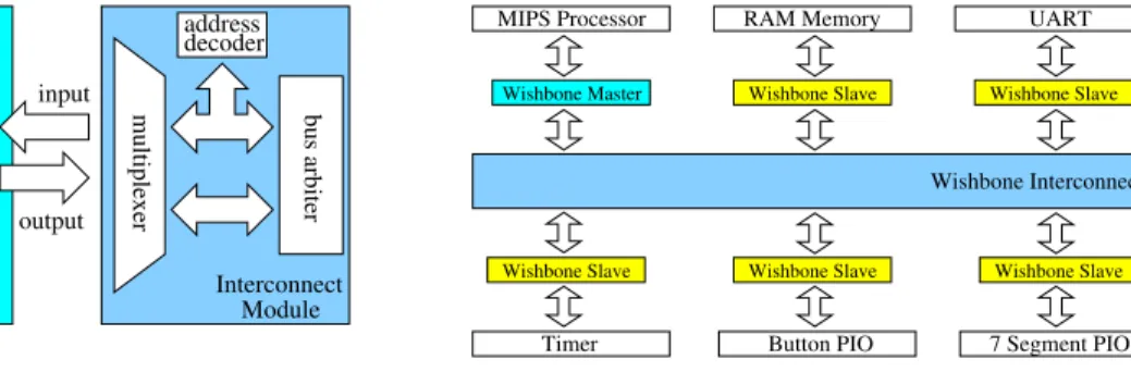
designs the set of the bus interface signals of the given IP core to be a subset of the signals provided by the given bus standard. In this case we can identify only one set of signals concerning the interconnection of the IP cores, namely that of the given bus standard. Further-more, the bus interface is integrated into the IP core and its functional logic, as shown in Fig. 1 for two IP cores with AMBA bus interfaces. For various reasons for the SoC engineer it is not always possible to use IP cores with the same bus interface in his design. Therefore, we propose to separate the bus interface of an IP core from its functional logic. After this step additional sets of signals can be identified as shown in Fig. 2. In this figure three types of bus modules are introduced: the master and the slave module which represent the mas-ter and the slave inmas-terface to the specific OCB and the interconnection logic module for the appropriate OCB. If an IP core plays both master and slave roles in bus transfers like it is the case in IP cores with DMA func-tionality this core is simultaneously connected with one master and one slave module. Similarly, the IP core can simultaneously be connected to multiple master or slave modules. Therefore, our approach supports any combination of master and slave modules connected to the OCB. In master and slave components a distinction is made between the set of original OCB defined sig-nals I and the set of external sigsig-nals E generated by the IP core. The set B={wei,weo,adri,adro,dati,dato,cs}
consists of the base signals needed for basic bidirec-tional communication over the OCB. The index next to the signal name denotes the direction of the signal rel-ative to the given module: i stands for input and o for output signals. Write enable, address, data, and chip se-lect signals are abbreviated with we, adr, dat, and cs, respectively. In the case that B⊂(E∩I)the IP core at least partially implements the current OCB interface. If
(E∩I)≡B only the minimal functionality possible is
IP Core {E} IP Core {E} IP Core {E} IP Core {E} IP Core {E} IP Core Interconnect module
{I} {I} {I}
{I} {I} {I}
Master module 1 Master module 2
{E}
Slave module 1 Slave module 2 Slave module n Master module n
Figure 2: The logical structure of an OCB.
supported with the help of the basis signals from the set
B.
∀e,i∈(E∩I): i :=e (1) The external signals e which are within the set E∩I
can simply be assigned to the respective internal signal
i, observing the right input/output relation. The signals
from the sets E\I and I\E have to be treated separately.
As an exemplification we now consider the question, how two IP cores with integrated AMBA interfaces can communicate over a Wishbone bus, see Fig. 1. The sig-nals from the set E\I must be treated as the so-called tag signals to keep as much as possible of the original
performance of the IP Core with its native AMBA bus interface. According to the Wishbone standard these signals are passed through the Wishbone interconnect to other modules like shown in Fig. 1. Control sig-nals like interrupts, errors, control status information etc. can also be integrated into the Wishbone intercon-nect with the help of the tag concept. According to the Wishbone specification [14] tags constitute a spe-cial class of signals which is intended for user enhance-ments to the Wishbone specification. In addition three tag types are defined, to indicate the precise timing to which the signal must conform. The tag types include the address tags, the data tags and the cycle tags. Parity information about the address or data transfer would be an example for address tag and data tag signals, respec-tively. Signals for a privileged access to the bus would be treated as a cycle tag signal. Thereby additional in-formation can be attached to an address transfer, a data transfer or a bus cycle. Because theHRESPsignal from AMBA AHB slave interface provides additional infor-mation on the status of a transfer likeOK,ERROR,RETRY,
andSPLITthe signal belongs to the set E\I and the data
tag typeTGD Owas chosen in Fig. 1. The signals from the set I\E must be assigned a default value in form of
a reasonable constant. For example, if no handshaking between a master and a slave module is needed, and the IP core connected to the slave module has no acknowl-edgement output signal, the corresponding input signal in the slave module is assigned a constant value of 1.
additional logic input output state machine Master or Slave Module input input output
multiplexer bus arbiter
decoder address
Interconnect Module
Figure 3: Internal bus modules’ structure.
The inner structure of a master or slave module from Fig. 3 consists of a state machine which implements the actual bus transfer protocol and some additional logic especially for mapping of external signals to internal signals according to the Equation (1). The interconnec-tion component in Fig. 3 consists of a bus arbiter, a mul-tiplexer which connects the master modules with slave modules according to the current arbitration scheme and the central address decoder which selects the appropri-ate slave module.
4.1
Integration into the Framework
The modules implementing the ideas mentioned above were designed and integrated into the overall frame-work. For each module several generic parameters can be specified graphically:
Interconnect Module. The width of the address and the data line for the interconnect module can be entered in 1-bit steps. The minimum width is 8 bit and the max-imum width was arbitrarily chosen to be 32 bit. Any change in the width of the interconnect module is au-tomatically propagated to the master and slave modules connected. These changes are mapped to the simulation models as well as to the generated VHDL files via the generic variable concept in VHDL.
Master Module. Master modules implement both the asynchronous and the synchronous data transfer [14]. This either can be specified at run-time by the IP core connected to the master module or it must be specified before the synthesis if the IP core does not implement the Wishbone interface.
Slave Module. The registers of the IP cores con-nected to the slave modules are used for memory mapped I/O. This means that the same bus is used to ad-dress both memory and I/O devices during input/output operations. The CPU instructions used to read and write to memory are also used in accessing I/O devices. The width of the address line for the slave module can also be specified graphically.
In the next Section we proceed with the implemen-tation details and synthesis results of the case study.
MIPS Processor UART
Timer Button PIO 7 Segment PIO
Wishbone Master
Wishbone Interconnect
Wishbone Slave Wishbone Slave
Wishbone Slave Wishbone Slave Wishbone Slave
RAM Memory
Figure 4: The implemented Wishbone OCB case study.
5
Case Study
In order to test our concept of a reconfigurable System-On-Chip, a design containing one processor which communicates with several dynamically configurable peripheral devices like GPIO (General Purpose Input/ Output) and UART (Universal Asynchronous Receiver/ Transmitter) over the Wishbone-compliant OCB was entered using the GUI of the ARCHITECTURECOM
-POSER. As a processor core a MIPS processor was used which was also specified using ARCHITECTURECOM
-POSER. The initial parameters of the modules used in the design are specified graphically and the peripheral devices as well as OCB modules are dynamically recon-figurable at run-time. Finally, the automatically gener-ated VHDL code for this design was synthesized on an Altera Cyclone FPGA.
The design consists of a MIPS processor in form of a soft IP core connected as a master to the Wishbone bus, an integrated 1 KByte RAM memory, UART module for external communication, a timer module as well as three general purpose I/O modules (see Fig. 4). None of the IP cores in the system has a built-in Wishbone bus interface. Only the signals from the base set B are available: we, adr, dat, and cs. The integrated memory has an asynchronous interface, thus the asynchronous communication mode was chosen. The whole design builds an embedded control system with external com-munication tasks accomplished by the UART module, the computational tasks run on the MIPS processor, and the user interaction performed over the GPIO modules.
5.1
Fast Simulation
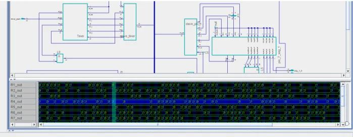
In order to verify the functional behavior of the spec-ified case study SoC design before synthesis, a stand-alone C++-compiled fast simulator of the whole de-sign was automatically generated in order to test dif-ferent scenarios. The structure of the generated simu-lator is similar to the structure of a conventional
Figure 5: Waveform fragment of the simulation.
Table 1: Simulation speed results for the case study SoC design.
Simulator name Simulation speed Modelsim 14 285 cycles/s
RASIM 83 333 cycles/s
on an event-driven model which is especially advan-tageous when simulating reconfigurable architectures where some signals may change only during the con-figuration phase. The main principle of the simulator includes the main simulation loop in which the stim-uli vectors are read from an external stimstim-uli file, the simulation routine sensitivity-update is called to per-form the current simulation cycle, and the selected trac-ing values are stored. The simulation results presented in the integrated graphical waveform viewer are shown in Fig. 5. Furthermore, the integrated design environ-ment allows for setting watch-points, i.e. register val-ues can be directly displayed within the registers of the schematic entry. This is very convenient during step-by-step architecture debugging. With the help of sev-eral optimization techniques based on graph theoretic approaches [19], a speedup of 6 was achieved compared to Modelsim, see Table 1. Because of the asynchronous communication mode the high potential of these tech-niques for synchronous designs [19], [20] could not be fully exploited in this case.
5.2
Design flow of the case study
The single steps, beginning with 1) the graphical archi-tecture entry, 2) generation of the simulation model, 3) compiling of the generated simulator, 4) fast simulation,
5) validation of the simulation results, 6) generation of the synthesizable VHDL code, 7) design entry into syn-thesis tool, and finally 8) the synsyn-thesis of the whole de-sign, as well as the corresponding time expenditure are
Table 2: Design steps and their processing times.
Design Step Tool Name Time (mm:ss)
STEP1 ARCHCOMP 20:00 STEP2 ARCHCOMP 00:01 STEP3 ARCHCOMP 00:05 STEP4 RASIM 00:06 STEP5 ARCHCOMP 15:00 STEP6 ARCHCOMP 00:01 Design time 35:13
STEP7 ALTERAQUARTUS 60:00
STEP8 ALTERAQUARTUS 10:15
Synthesis time 70:15
Overall time 105:28
summarized in Table 2. In the first step the design was graphically entered into our tool. Then the simulation model of the design was automatically generated. In the third step the simulation model was compiled with the GCC 3.3-compiler on a Pentium 4, 2 GHz machine under Linux operating system. After this, the stand-alone simulator was run on the same machine and the simulation results were analyzed in the fifth step. Syn-thesizable VHDL-code was automatically generated in the next step. So far, the design time took us 35 minutes. The synthesis of the design was performed on the same
machine under Windows XP operating system with the help of the Altera Quartus II v.4 software for the
Cy-clone EP1C20F400C7 FPGA. The design entry, project
creation, pin assignments, and the definition of several synthesis options took us 60 minutes. The synthesis of the design took another 10 minutes. The overall time for the creation of the hardware part of our SoC design was only 105 minutes.
Table 3: Synthesis results for the case study SoC design of Wishbone bus interfaced modules.
Bus Module Logic Cells Registers 1 master and 6 slaves 75 0
multiplexer and ar-biter
79 2
address decoder 14 0
whole SoC design 4097 1536
5.3
Synthesis Results
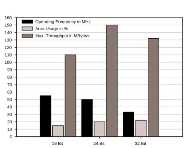
For the synthesized SoC with 16-bit address and 24-bit data line width the results from Table 3 were obtained. Altera Quartus II v. 4 software was used for the synthe-sis. The synthesis results show only a small logic cell demand for the introduced bus modules, see Table 3. As only an asynchronous mode for communication was chosen no registers and no state machines in the master or slave components were generated and consequently no registers were synthesized for these modules. The design runs with the frequency of 50 MHz. The peak throughput of the bus module is therefore 150 MByte per second. It can be increased if a synchronous burst mode for data transfer is chosen. By the use of the synchronous transmission scheme the overall frequency can further be increased and the use of burst mode also gives a performance gain by reducing the overall cycle number, needed to transfer the given amount of data. To explore the impact of the data path width of the OCB bus on the area usage and the frequency of the design, the width of the data path was varied in the first step in Table 2 and then steps 6 to 8 were performed for 16, 24 and 32 bit widths. The results are summarized in the Fig. 6. According to the results, the width of 24 bits should be chosen for maximum throughput.
6
Conclusions and Future Work
The need for an integrated environment for architecture specification, simulation and synthesizable HDL code generation is existent and urgent. In this paper such a
Data Path Width
16 Bit 24 Bit 32 Bit 0 10 20 30 40 50 60 70 80 90 100 110 120 130 140 150 160 Operating Frequency in MHz Area Usage in % Max. Throughput in MByte/s
Figure 6: Operating frequency, area usage and maxi-mum throughput for different data path widths.
software framework, ARCHITECTURECOMPOSER, was presented. It allows a graphical specification, cycle ac-curate simulation for convenient system validation and debugging respectively, and finally the automatic HDL code generation. In connection with the integrated OCB and peripheral components, complex SoC designs can be implemented as well. In the case study a Wishbone-compliant OCB was implemented and tested in a stan-dard SoC system with a MIPS processor and peripheral devices on an Altera Cyclone FPGA. With the integra-tion of the Wishbone OCB and peripheral components like UART, PIO, and timer into the component library of ARCHITECTURECOMPOSERa complete solution for the rapid prototyping of systems on a chip is now avail-able. In the future, we would like to automate the syn-thesis of bus protocols using an approach similar to the one presented in [21] and [22]. Furthermore, we plan to use ARCHITECTURECOMPOSERin practical courses to inspire students with interest in hardware architecture and reconfigurable computing.
References
[1] Ryu, K., Mooney, V.: Bus Generation for Multi-processor SoC Design. In: Proceedings of Design, Automation and Test in Europe (DATE), Munich, Germany (2003)
[2] Martin, G., Schirrmeister, F.: A Design Chain for Embedded Systems. Computer 35(3) (2002) 100– 103
[3] Shin, C., Kim, Y., Chung, E., Choi, K., Kong, J., Eo, S.: Fast Exploration of Parameterized Bus
Architecture for Communication-Centric SoC De-sign. In: Proceedings of Design, Automation and Test in Europe (DATE), Paris, France (2004) [4] Zhu, X., Malik, S.: A Hierarchical Modeling
Framework for On-Chip Communication Archi-tectures. In: Proceedings of the 2002 IEEE/ACM International Conference on Computer-aided De-sign (ICCAD), San Jose, California, ACM Press (2002) 663–671
[5] Ces´ario, W., Lyonnard, D., Nicolescu, G., Paviot, Y., Yoo, S., Jerraya A., A., Gauthier, L., Diaz-Nava, M.: Multiprocessor SoC Platforms: A Component-Based Design Approach. IEEE Des. Test 19(6) (2002) 52–63
[6] Altera: Quartus II Handbook, Version 4, Section I, SOPC Builder Features. (2005)
[7] Fraboulet, A., Risset, T., Scherrer, A.: Cycle Accurate Simulation Model Generation for SoC Prototyping. In: Computer Systems: Archi-tectures, Modeling, and Simulation, 4th Interna-tional Samos Workshop, SAMOS, Proceedings. Volume 3133 of Lecture Notes in Computer Sci-ence (LNCS)., Island of Samos, Greece, Springer (2004) 453–462
[8] VSI Alliance: Virtual component interface stan-dard OCB specification 2, Version 2.0. On-Chip Bus Development Working Group (2001)
[9] MentorGraphics Modelsim:
(http://www.model.com)
[10] Ryu, K., Shin, E., Mooney, V.: A Comparison of Five Different Multiprocessor SoC Bus Archi-tectures. In: Proceedings of the Euromicro Sym-posium on Digital Systems Design, Washington, DC, USA, IEEE (2001) 202
[11] IBM: IBM On-Chip Peripheral Bus Architecture Specifications, Version 2.1. IBM (2000)
[12] Arm Ltd.: Amba Specification Revision: 2.0. (1999)
[13] Altera: Avalon Bus Specification Reference Man-ual. (2003)
[14] Silicore Corp.: Wishbone System-on-Chip (SoC) Interconnection Architecture for Portable IP Cores. Revision: B.3. Silicore Corp. (2002) [15] OCP International Partnership: OCP Specification
Revision: 2.0. OCP-IP (2003)
[16] Fischer, D., Teich, J., Thies, M., Weper, R.: BUILDABONG: A Framework for Architec-ture/Compiler Co-Exploration for ASIPs. Jour-nal for Circuits, Systems, and Computers, Spe-cial Issue: Application Specific Hardware Design (2003) 353–375
[17] Fischer, D., Teich, J., Thies, M., Weper, R.: Ef-ficient Architecture/Compiler Co-Exploration for ASIPs. In: ACM SIG Proceedings International Conference on Compilers, Architectures and Syn-thesis for Embedded Systems (CASES 2002), Grenoble, France (2002) 27–34
[18] Fischer, D., Teich, J., Weper, R.: Hierarchi-cal modeling and simulation of embedded proces-sors using ASMs. In: International Workshop on Software and Compilers for Embedded Systems (SCOPES01), St. Goar, Germany (2001)
[19] Kupriyanov, A., Hannig, F., Teich, J.: Au-tomatic and Optimized Generation of Compiled High-Speed RTL Simulators. In: Proceedings of Workshop on Compilers and Tools for Con-strained Embedded Systems (CTCES), Washing-ton, DC, U.S.A. (2004)
[20] Kupriyanov, A., Hannig, F., Teich, J.: High-Speed Event-Driven RTL Compiled Simulation. In Pi-mentel, A., Vassiliadis, S., eds.: Computer Sys-tems: Architectures, Modeling, and Simulation, 4th International Samos Workshop, SAMOS, Pro-ceedings. Volume 3133 of Lecture Notes in Com-puter Science (LNCS)., Island of Samos, Greece, Springer (2004) 519–529
[21] Ihmor, S., Visarius, M., Hardt, W.: A Design Methodology for Application-Specific Real-Time Interfaces. In: Proceedings of IEEE International Conference on Computer Design (ICCD): VLSI in Computers & Processors. IEEE International Con-ference on Computer Design, Freiburg, Germany (2002)
[22] Passerone, R., Rowsan, J., Sangiovanni-Vincentelli, A.: Automatic Synthesis of Interfaces between Incompatible Protocols. In: Proceedings of the 1998 Conference on Design Automation (DAC), Los Alamitos, CA, ACM/IEEE (1998) 8–13