technology for the design of its feed network and longitudinal slots in the SIW top metallic surface to drive the array antenna elements. Dielectric cubes of low-permittivity material are placed on top of each 1 4 an-tenna array to increase the gain of the circular patch anan-tenna elements. This new design is compared to a second 4 4 antenna array which, in-stead of dielectric cubes, uses vertically stacked Yagi-like parasitic director elements to increase the gain. Measured impedance bandwidths of the two 4 4 antenna arrays are about 7.5 GHz (94.2–101.8 GHz) at 18 1 dB gain level, with radiation patterns and gains of the two arrays remaining nearly constant over this bandwidth. While the fabrication effort of the new array involving dielectric cubes is significantly reduced, its measured radi-ation efficiency of 81 percent is slightly lower compared to 90 percent of the Yagi-like design.
Index Terms—Antenna array, substrate integrated waveguide (SIW), W-band antenna, Yagi-like antenna.
I. INTRODUCTION
A wide range of applications has attracted growing attention from industry and academia to the W-band (75–110 GHz) [1]. Operating fre-quencies of wireless communication systems have increased in order to provide access to a less crowded part of the electromagnetic spectrum and also a wider bandwidth for data transmissions [2]. As shown in [3], the atmospheric absorption is much lower at W-band frequencies than at 60 GHz. Therefore, given a point-to-point wireless communication link, the W-band spectral window offers the possibility of gigabyte data transmission over several kilometers in normal weather conditions [4]. Wide bandwidth and low atmospheric loss features permit the imple-mentation of high resolution and long range detectors or sensors [5], which may be used in helicopter or aircraft collision avoidance radar [6], civil avoidance security [7], passive millimeter wave imaging [8], and radar sensors [9]. One of the most critical parts of such systems are low-cost, low-profile and lightweight antenna components.
Although various microstrip-fed antenna arrays have been studied and used, these configurations suffer from severe losses as frequency
Manuscript received May 14, 2011; revised July 20, 2011; accepted August 31, 2011. Date of publication December 16, 2011; date of current version March 02, 2012.
N. Ghassemi and K. Wu are with the Poly-Grames Research Center and the Center for Radiofrequency Electronics Research of Quebec (CREER), Depart-ment of Electrical Engineering, Ecole Polytechnique, University of Montreal, Montreal, QC H3V 1A2, Canada (e-mail: [email protected]; [email protected]).
S. Claude is with the National Research Council of Canada, Herzberg Institute of Astrophysics, Victoria, BC V9E 2E7, Canada (e-mail: Stephane. [email protected]).
X. Zhang is with the Department of Electrical and Computer Engineering, Concordia University, Montreal, QC H3G 1M8, Canada (e-mail: xzhang@ece. concordia.ca).
J. Bornemann is with the Department of Electrical and Computer Engi-neering, University of Victoria, Victoria, BC V8W 3P6, Canada (e-mail: [email protected]).
Color versions of one or more of the figures in this communication are avail-able online at http://ieeexplore.ieee.org.
Digital Object Identifier 10.1109/TAP.2011.2180346
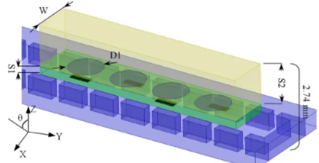
Fig. 1. Layout of a 124 antenna array (S1 = 0:1 mm,S2 = 2 mm,W =
1:24 mm, andD1 = 0:75 mm).
increases to the millimeter-wave range [10]. Recently, substrate-inte-grated waveguide (SIW) technology has been proposed to provide a low-cost alternative for millimeter-wave applications [11]. SIW enjoys not only the advantages of rectangular waveguide features but also of-fers other benefits such as low cost, compact size, light weight, and easy fabrication using PCB or similar processes. Furthermore, SIWs can easily be connected to microstrip and coplanar waveguides utilizing a wideband transition [12].
High gain and wide bandwidth are two of the key requirements for a large number of antenna designs. To increase antenna gain, the use of a substrate with either permittivity"r 1or permeabilityr 1is proposed in [13]. However, the bandwidth is inversely proportional to the gain, and material with"r 1is generally expensive and lossy.
Due to its directive radiation pattern, the Yagi antenna has been widely applied in communication systems. However, it requires a boom to structurally support individual antenna elements [14]. To eliminate the boom, printed Yagi antennas were demonstrated in X band [15], [16], with radiation in a plane parallel to the substrate. But such antennas have a very large footprint. In many applications, an antenna is desired to have a broad radiation pattern in the plane perpendicular to the substrate. Therefore, an interesting approach is to use stacked director elements in a Yagi-like arrangement to increase the gain of printed antennas [17]. Later, this technique has been used in a multilayer Yagi-like microstrip antenna at 31 GHz [18], a dipole stacked Yagi antenna at 5.8 GHz [19], a dual polarized circular patch Yagi antenna at 5.8 GHz [19] and a stacked Yagi antenna at 60 GHz [20] with a very small footprint.
In this communication, we present a different design of low-cost and high-efficiency 424 antenna arrays for applications close to 97 GHz. SIW technology is used to feed the antenna elements through longitu-dinal slots in the top metallization. The main difference compared to a similar Yagi-like array [20], which has been redesigned and is also presented for comparison, is that the multi-layered Yagi arrangement is replaced by a dielectric block, thus significantly simplifying the fab-rication process. Compared with previous millimeter-wave SIW slot antennas [21]–[23], the antenna structures presented in this communi-cation result in higher gain, larger bandwidth and higher radiation effi-ciency with a more stable (less dispersive) gain within the operational bandwidth.
II. DESIGN
The proposed 424 W-band antenna array consists of four 124 antenna arrays as shown in Fig. 1. Each 124 element has three basic layers.
The bottom layer is the SIW feed network, which is designed using a 20 mil Rogers/Duroid 6002 substrate. It is shown in Fig. 2 for the entire 0018-926X/$26.00 © 2011 IEEE
Fig. 2. Layout of the 424 feed network and dimensions of the slots (SW =
0:24 mm,SL = 0:6 mm,VW = 0:254 mm,VL = 0:75 mm,W1 =
1:24 mm,W2 = 1:24 mm, andW3 = 1:55 mm).
424 array including the one-to-four power divider. The four circular antenna elements in Fig. 1 are fed in phase by four longitudinal, linearly polarized slots in the top metallization of the SIW. Their centers are half a wavelength apart, which amounts to 1.375 mm at the center frequency of 97 GHz. The SIWs are terminated by short circuits that are three quarter wavelengths away from the center of the last slot in order to align the slots at the peaks of the standing wave in the SIW. The design procedure is similar to the work presented in [22], and the reader is referred to [22] for further details.
The middle layer consists of circular patches of diameter D1 which are placed over the slots on an Ultralam 3850 substrate of thickness S1 and dielectric constant of 2.9. The resonant frequency of the patches depends on the patch diameters and the dielectric constant of its top and bottom layers [24]. To increase the bandwidth of the antenna, the resonant frequencies of the patches and slots are set to be close to each other. To reach the maximum gain and bandwidth, the dimension of the circular patches, the slots, and the thickness of the Ultralam 3850 substrate are optimized with Ansoft HFSS.
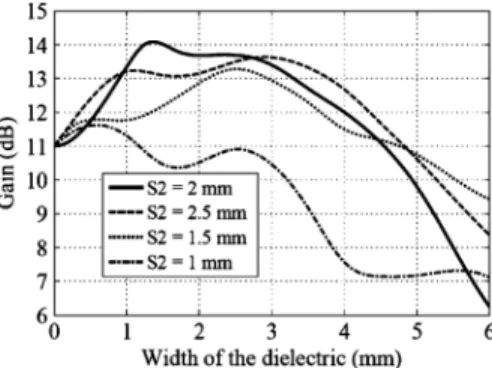
The top layer of the 124 array is a dielectric cube with relative permittivity of 2.2, which is placed on top of the patches to increase the gain of the antenna. It is found that width W and thickness S2 (c.f. Fig. 1) of this cube have a strong effect on the radiation pattern and gain of the antenna. Fig. 3 shows the simulated gain versus width W of the cube at different thicknesses S2 of the array. It is shown that the maximum gain of 14 dB is obtained using a dielectric cube with dimen-sionsS2 = 2 mmandW = 1:24 mm, instead of 11 dB without such cube. Therefore, a 3 dB gain increase is obtained through the addition of the dielectric cube.
Fig. 4 shows the normalized radiation pattern of the antenna with and without the dielectric cube(W = 1:24 mm). It is observed that the antenna’s directivity is increased by adding the cube.
SimulatedjS21jandjS11jplots of the Y- and T-shaped junctions are shown in Fig. 5. Note that the reflection of the T junction is higher than that of the Y junction due to the 90 degree bends in this structure. In order to decrease the mutual coupling between the four 124 arrays, they were separated by a distance of0:95. Due to the high directivity of the 124 arrays, the level of grating lobes, which results from an increase in separation from0:5to0:95will be less than the side lobe level.
(S2) of 1, 1.5, 2, and 2.5 mm for a 124 array antenna. Note that dielectric or metallic losses are not considered in this simulation.
Fig. 4. Normalized radiation pattern in the (a) XZ (E-) plane, (b) YZ (H-) plane (c.f. Fig. 1), of the 124 antenna array considering the effect of the dielectric cube; solid lines: with dielectric cube, and dashed: without dielectric cube.
Fig. 5. SimulatedjS jandjS jof the T-shaped and Y-shaped junctions.
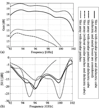
Fig. 6 illustrates the effect of the circular patches and dielectric cube on gain (Fig. 6(a)) andjS11j(Fig. 6(b)) of the 424 antenna array. It is shown in Fig. 6(b) that the bare slot array (structure of Fig. 1 without the dielectric cube and circular patches) has one resonant frequency with 3% impedance bandwidth. By adding the circular patches on the top of the slots (structure of Fig. 1 without the dielectric cube), the bandwidth of the structure is increased due to the fact that the resonant frequencies of the patches and slots are set to be close to each other. Although adding the circular patches does not have a significant ef-fect on the gain of the antenna, it increases the bandwidth to 7.2% (7 GHz). Fig. 6(a) also shows that adding the dielectric cube on top of the patches increases the gain of the antenna array by 3.5 dB. Fig. 6(b) shows that the dielectric cube does not have a significant effect on the bandwidth of the antenna. For the above investigation of the effect of patches and dielectric cubes, the dimensions of the patches and slots
Fig. 6. Simulated gain (a) andjS j(b) of the 424 antenna array considering the effect of the dielectric and metallic losses.
were changed to be compatible with the structure because the resonant frequency of the circular patch depends on the dielectric constant of the top and bottom layers.
Note that for the slot array and the structure without the dielectric cube, metallic and dielectric losses are considered in the simulation. Simulated results show that including metallic loss decreases the gain of the antenna array by 0.14 dB while including dielectric loss de-creases the gain by 1.18 dB; both losses do not reduce the bandwidth. To estimate the dielectric loss tangent of the substrate at 97 GHz, two different lengths SIW are used; one to calibrate the vector analyzer, and the other to estimate the total loss. Then HFSS software is used to compare the simulatedjS21jwith the measured results. This method was used in [25] to estimate the dielectric loss tangent at 60 GHz. It is concluded that the metallic and dielectric losses do not have a signifi-cant effect on the bandwidth of the antenna array. However, it is found that the radiation efficiency is decreased from 97% to 85% due to the dielectric and metallic losses.
In order to compare the 424 W-band array with an antenna using a different top layer, another array based on a vertically stacked Yagi-like antenna has been designed and is presented in this work for compar-ison. The design procedure is similar to [20] with the exception that instead of circular disks, circular rings are employed as directors. The layout of a 124 W-band array is shown in Fig. 7.
The bottom and second layers are identical to those previously pre-sented above. The ring shaped director elements are vertically stacked over the circular patch. The director elements increase the gain of the circular patch and provide a nearly constant radiation pattern across the bandwidth of the antenna. The radius of and spacing between the direc-tors are optimized using HFSS. Detailed design procedures are similar to those presented in [17]–[20]. However, in this work and to increase the bandwidth of this antenna compared to [20], the resonant frequen-cies of the patches and slots are also set to be close to each other, as discussed earlier. The director elements are etched on low-cost Rogers/ Duroid 5880 substrate with thickness of0:12d(G2 = 10 mil)and dielectric constant of 2.2.
Fig. 7. Layout of the 124 vertically stacked Yagi-like antenna array (G1 =
0:1 mm,G2 = 0:25 mm,D1 = 0:75 mm,D2 = 0:65 mm,D3 =
0:64 mm, andD4 = 0:3 mm).
Fig. 8. Photograph of the fabricated 424 antenna array with dielectric cubes; (a) top view, (b) bottom view, (c) antenna under test.
Fig. 9. Measured and simulated reflection coefficients of the 424 antenna array with dielectric cubes.
III. RESULTS
A low-cost standard PCB process is used to fabricate the proposed 4 2 4 antenna array with dielectric blocks. Fig. 8 shows the top (Fig. 8(a)), the bottom views (Fig. 8(b)) as well as the array under test
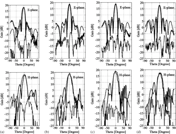
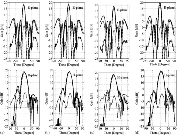
Fig. 10. Simulated and measured co-polarization and measured cross-polarization patterns of the dielectric-cube array in the E- and H-planes at (a) 95.25 GHz, (b) 97 GHz, (c) 98.75 GHz, and (d) 100.5 GHz. Solid: measured, dashed: simulated, and dotted: measured cross-polarization.
including the WR10-to-SIW transition (Fig. 8(c)). The SIW feed net-work is fabricated on a rectangular (30 mm220 mm) Rogers/Duroid 6002 substrate. The simulated and measured SIW losses are 0.52 dB per centimeter at 97 GHz. The dielectric cubes are made of two layers of low-cost Rogers/Duroid 5880 substrates, one 20 mil thick and the other 60 mil thick. The two layers are glued together to achieve the desired thickness of 80 mil. The adhesive is an epoxy with dielectric constant of 3.5 and thickness less than 5m. Note that the effect of the adhesive is considered in the simulation results of this communication. To avoid the excitation of surface waves, arrays of metallic via holes are placed around the dielectric cubes.
The reflection coefficient of the prototype antenna is measured by an Anritsu 3739C vector network analyzer. A wideband transition be-tween rectangular waveguide (WR10) and SIW (e.g., [27], [28]) is used to measure the antenna parameters. Fig. 9 shows the measuredjS11j performance. The measured bandwidth is 7.6 GHz (94.2–101.8 GHz) which is similar to the simulation results. This value of 7.7 % band-width represents a considerable improvement to what was previously reported, e.g., 2.7% [21], 4.1% [22], and 2% [23]. As shown in Fig. 9, a frequency shift of about 1.4% towards higher frequencies occurs. It has been shown that the resonant frequencies of the slots in the SIW slot antennas are very sensitive to the positioning of the slots [23]. It has also been indicated that the measurement probes can cause frequency shifts at 60 GHz [26]. The observed discrepancy between the simulated and measuredjS11jresults can be attributed to the combined effect of inaccuracy of the patches and slot placement, the WR10 to SIW transi-tion, and the inaccuracy of the dielectric constant. This frequency shift is taken into account when plotting radiation patterns and gain, i.e., the measured radiation pattern is plotted at 97 GHz in comparison with the simulated radiation at 95.6 GHz.
Fig. 11. Photograph, measured and simulatedjS j, of the 424 vertically Yagi-like antenna array.
Fig. 10 shows the simulated and measured E- and H-plane radia-tion patterns at frequencies of 95.25, 97, 98.75 and 100.5 GHz. Good agreement can be observed between simulated and measured patterns. The side lobe level is better than 10 dB in the E- plane. As shown in Fig. 10, there are discrepancies between the measured and simulated ra-diation patterns, especially in the H-plane. These discrepancies are due to the combined effect of the fabrication inaccuracy and the waveguide to SIW transition (c.f. Fig. 8(c)). One of the advantages of this antenna is that a constant gain of 1861 dB is obtained over the7.5 GHz bandwidth. In addition, the measured cross polarization is 23 dB or better over most of the bandwidth of 7.5 GHz. The estimated radiation efficiency from the measured gain and directivity, e.g., [22], is 81% at 95.25 GHz, while the simulated radiation efficiency is 85%. Note that the dielectric, metallic, and mismatch losses have been considered in the simulation results.
Fig. 12. Simulated and measured co- and cross-polarization patterns of the Yagi-like array in E- and H-planes at (a) 95.25 GHz, (b) 97 GHz, (c) 98.75 GHz, and (d) 100.5 GHz. Sold: measured, dashed: simulated and dotted: measured cross-polarization.
Fig. 11 shows a photograph of the vertically stacked Yagi-like 42 4 antenna array. To reduce the mutual coupling between the 124 ar-rays, the dielectric between them is removed. The measured reflection coefficient of the 424 vertically stacked Yagi-like antenna array is also shown in Fig. 11. The measured bandwidth of the antenna array is 7.5 GHz (about 7.6%) and is comparable to that obtained for the array using dielectric cubes. Again, we observe a 1.7% (1.65 GHz) frequency shift which we attribute to the reasons discussed earlier in this section. As previously, this frequency shift is taken into account when plotting radiation patterns.
The measured E- and H-plane radiation patterns of the vertically stacked Yagi-like antenna array are shown in Fig. 12 at frequencies of 95.25, 97, 98.75 and 100.5 GHz. Good agreement is observed between the simulated and measured responses. The antenna has a constant gain of 18 dB61 dB across the 7.5 GHz bandwidth. The measured side lobe levels are 14 and 11 dB in the H- and E-plane, respectively, at 100.5 GHz. The discrepancies between simulated and measured side lobe levels are due to the combined effect of the fabrication inaccuracy and the waveguide to SIW transition.
The measured cross polarization of the antenna array is better than 17 dB over most of the 7.5 GHz bandwidth. The estimated radiation efficiency from the measured gain and directivity is 90% at 98.75 GHz which is similar to the simulation results. The dielectric, metallic, and mismatch losses have been considered in the simulation.
IV. CONCLUSION
Two low-cost and high-efficiency antenna arrays for applications in the W-band are proposed and demonstrated using standard low-cost PCB processing. SIW technology is employed to feed the antenna ele-ments through the slots on the top metallic surface. One SIW T-junc-tion and two Y-JuncT-junc-tions are used to realize a four-way power divider
to feed the 424 antenna arrays. The two 424 array prototypes are implemented using Rogers RT/Duroid substrate with low-cost multi-layer PCB processing. It is found that the dielectric and metallic losses decrease the antenna gain by 1.3 dB, and also do not have a signifi-cant effect on the bandwidth. For the new 424 antenna array, a di-electric cube is placed on top of the 124 arrays of circular patches to increase the gain of the antenna. This dielectric cube is made of a low dielectric constant material and leads to an increased antenna gain of 3 dB. The measured gain of the 424 antenna array is 186 1 dB over a 7.7% bandwidth centered at 98 GHz. The second 424 antenna array is similar to a previously reported component and uses vertically stacked Yagi-like elements as directors. However, both gain and bandwidth have been increased to 19 dB and7.5 GHz, respec-tively. Moreover, 90 percent radiation efficiency is estimated from the measured radiation patterns and gain.
Both structures result in similar bandwidths and gains, though the radiating elements between the two designs are different. The array with dielectric cubes consists of only three layers whereas the second antenna (Yagi-like) requires six layers. Thus the fabrication process and cost of the first antenna is almost half of that of the Yagi-like antenna. However, the Yagi-like antenna is 1.12 mm thinner. Compared with the regular SIW slot array antennas, the two proposed antennas have higher gain and broader bandwidth. This work shows that it is possible to design high gain antenna arrays with high radiation efficiency in W-band by utilizing SIW circuitry.
ACKNOWLEDGMENT
The authors wish to tank T. Antonescu for his help in fabrication the prototype, and Dr. T. Djerafi for providing the WR10 to SIW transition.
[6] C. C. Ling and G. M. Rebeiz, “A 94 GHz planar monopulse tracking receiver,”IEEE Trans. Microwave Theory Tech., vol. 42, no. 10, pp. 1863–1871, Oct. 1994.
[7] R. J. Hodges, Badley, and Tarsier, “A millimeter wave radar for air-port runway debris detection,” presented at the Eur. Radar Conf., Am-sterdam, 2004.
[8] L. Yujiri, M. Shoucri, and P. Moffa, “Passive millimeter wave imaging,”IEEE Microwave Mag., vol. 4, pp. 39–50, 2003.
[9] E. Moldovan, S. O. Tatu, T. Gaman, K. Wu, and R. G. Bosisio, “A new 94-GHz six-port collision avoidance radar sensor,”IEEE Trans. Microwave Theory Tech., vol. 52, no. 3, pp. 751–759, Mar. 2004. [10] K. Wu, “Substrate Integrated Circuits (SICs) for low-cost high-density
integration of millimeter-wave wireless systems,” inProc. RWS2008, Jan. 2008, pp. 683–686.
[11] D. Deslandes and K. Wu, “Integrated microstrip and rectangular wave-guide in planar form,”IEEE Microwave Wireless Comp. Lett., vol. 11, pp. 68–70, Feb. 2001.
[12] S. Yang, “Antennas and Arrays for Mobile Platforms—Direct Broad-cast Satellite and Wireless Communication,” Ph.D. dissertation, Uni-versity of Tennessee, Knoxville, 2008.
[13] N. G. Alexopoulos and D. R. Jackson, “Gain enhancement methods for printed circuit antennas,”IEEE Trans. Antennas Propag., vol. AP-33, pp. 976–987, Sep. 1985.
[14] W. L. Stutzman and G. A. Thiele, Antenna Theory and Design. New York: Wiley, 1981.
[15] Y. Qian, W. Deal, N. Kaneda, and T. Itoh, “Microstrip-fed quasi-Yagi antenna with broadband characteristics,”Electron. Lett., vol. 34, pp. 2194–2196, Nov. 1998.
[16] G. Zheng, A. A. Kishk, A. B. Yakovlev, and A. W. Glisson, “Simplified feed for a modified printed Yagi antenna,”Electron. Lett., vol. 40, no. 8, pp. 464–465, Apr. 2004.
[17] A. Hoorfar, “Analysis of a “Yagi-like” printed stacked dipole array for high gain applications,”Microwave Opt. Technol. Lett., pp. 317–321, April 1998.
[18] A. Hoorfar, “Evolutionary programming in electromagnetic optimiza-tion: A review,”IEEE Trans. Antennas Propag., vol. 55, pp. 523–537, Mar. 2007.
[19] O. Kramer, T. Djerafi, and K. Wu, “Vertically multilayer-stacked Yagi antenna with single and dual polarizations,”IEEE Trans. Antennas Propag., vol. 58, pp. 1022–1030, Apr. 2010.
[20] O. Kramer, T. Djerafi, and K. Wu, “Very small footprint 60 GHz stacked Yagi antenna array,”IEEE Trans. Antennas Propag., accepted for publication.
[21] Z. Li and K. Wu, “24-GHz frequency-modulation continuous-wave radar front-end system-on-substrate,”IEEE Trans. Microwave Theory Tech., vol. 56, pp. 278–285, Feb. 2008.
[22] X.-P. Chen, K. Wu, L. Han, and F. He, “Low-cost high gain planar antenna array for 60-GHz band applications,”IEEE Trans. Antennas Propag., vol. 58, pp. 2126–2129, June 2010.
[23] D. Stephens, P. R. Young, and I. D. Robertson, “W-band substrate in-tegrated waveguide slot antenna,”Electron. Lett., vol. 41, no. 4, pp. 165–167, Feb. 2005.
[24] J. R. James and P. S. Hall, Handbook of Microstrip Antennas. London, U.K.: Peregrinus, 1989.
[25] D. Liu, B. Gaucher, U. Pfeiffer, J. Grzyb, and Hoboken, Advanced Mil-limeter-Wave Technologies. NJ: Wiley, 2009, pp. 167–170. [26] H. Vettikalladi, O. Lafond, and M. Himdi, “High-efficient and
high-gain superstrate antenna for 60-GHz indoor communication,”IEEE An-tennas Wireless Propag. Lett., vol. 8, pp. 1422–1425, 2009.
[27] T. Djerafi, “Étude et Réalisation de Matrices à Commutation de Fais-ceaux en Technologie Guide d’Onde Intégrée aux Substrats,” Ph.D. dis-sertation, École Polytechnique de Montréal, Montreal, Canada, 2011.
Abstract—Antenna polarization states always vary with scan direction. Here this phenomenon is called spatial polarization characteristic (SPC) of antenna. Based on the single polarized radar antenna, by sufficiently uti-lizing of the inherent polarization property of antenna (i.e. the property that polarization state is not a constant but a function of antenna’s spa-tial scanning direction), a novel polarization scattering matrix (PSM) mea-surement method is established. This method has the following advantages: (i) It does not need dual orthogonal polarization channels; (ii) the PSM of target can be obtained just by using the prior knowledge of SPC and by im-proving the signal processing mode of received radar signal. The modern radar systems can make use of this property in its measurement of target polarization scattering property in the searching or angle tracking stage.
Index Terms—Beam scanning, cross polarization, polarization scattering matrix (PSM), radar antenna, spatial polarization characteristic (SPC).
I. INTRODUCTION
Polarimetry is an important trend in the development of modern radar. As key feature information of target echo, polarization infor-mation has played an important role in meteorological sounding, geo-graphical remote sensing [1],[2], target polarization detection [3], [4], polarization enhancement [5], polarization filtering [6], polarization anti-jamming and target recognition [7]–[9]. How to acquire polariza-tion informapolariza-tion is undoubtedly a basic problem in the investigapolariza-tion of the characteristics of targets. Nowadays the techniques for measuring polarization scattering property of the target are the key for polarization radar realization, but such techniques face challenges in engineering applications. According to antenna theory, for a given frequency and space point in the far-field area, antenna has a predefined polarization direction [10]. At constant frequency, the antenna polarization of radi-ation field varies with different observradi-ation directions, indicating that the antenna polarization is a function of the spatial direction. The phe-nomenon of antenna polarization changing in radiated space can be re-ferred to as spatial polarization characteristic (SPC) of antenna. In this communication, antenna polarization slow variable property is used and taken into account in polarization signal processing technology. By doing so a novel method for measuring PSM is introduced. This
Manuscript received December 30, 2010; revised September 06, 2011; ac-cepted September 12, 2011. Date of publication December 16, 2011; date of current version March 02, 2012. This work was supported in part by the State Key Program of National Natural Science of China (Grant No. 60736006), the Youth Science Program of National Natural Science of China under Grant No. 60802078), and in part by Hunan Provincial Innovation Foundation for Post-graduate (CX2009B010).
The authors are with the Electronic Science and Engineering School, NUDT, Hunan 410073, China (e-mail: [email protected]).
Color versions of one or more of the figures in this communication are avail-able online at http://ieeexplore.ieee.org.
Digital Object Identifier 10.1109/TAP.2011.2180321 0018-926X/$26.00 © 2011 IEEE