S- 1 -
Supporting information
Highly Efficient Microcavity Organic Light
-
Emitting Devices with
Narrow
-
Band Pure UV Emission
Jie Lin†, Xiaoyang Guo†, Ying Lv†, Xingyuan Liu*†,‡, Yue Wang*§
†
State Key Laboratory of Luminescence and Applications, Changchun Institute of
Optics, Fine Mechanics and Physics, Chinese Academy of Sciences, Changchun
130033, Jilin, China.
‡
Center of Materials Science and Optoelectronics Engineering, University of Chinese
Academy of Sciences, Beijing 100049, China
§
State Key Laboratory of Supra molecular Structure and Materials, Jilin University,
Changchun 130012, China
S- 3 -
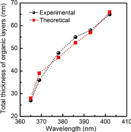
Figure S3. The experimental and theoretical thickness of organic layers inside
S- 5 -
Figure S4. The EL spectra of microcavities I, II, III, IV with EL peaks at 366.2, 378.8,
386.0 and 392.2 nm, corresponding to the FWHM of 17.0, 12.9, 10.0 and 9.95 nm,
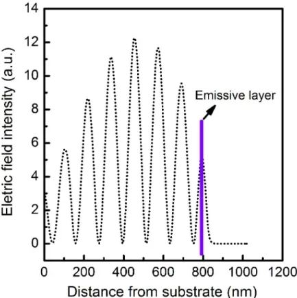
Figure S5. The electric field distribution inside the 366.4 nm UV mirocavity OLED.
S- 7 -
S- 9 -
S- 11 -
Table S1. Thermal, electrochemical and photophysical data of Tol-PPI
a)
Tm/b)Tg/c)Td5/oC λmax, abs/ nmd) λem/ nmd) HOMO/LUMO/eVe)
194/64/336 263, 311 387, 374 -5.58/-2.24
a) Tm: melting temperature; b) Tg: glass transition temperature; Td5: decomposition
temperature corresponding to 5% weight loss; d) Measured in CHCl3; e) The HOMO
and LUMO energies were determined from cyclic voltammetry and absorption data.
Table S2. Summary of UVOLEDs performances. devices λmax EL a) (nm) EQE b) (%) @ 100cd/m2 max. irradiance (mW/cm2) max. EQE ( %) VTc) (V) device A 378, 392 1.96 13.37 5.43 @ 5.35 μW/cm2 3.58 device B 392 2.04 10.55 3.69 @ 7.39 μW/cm2 3.86 device C 378 1.04 9.56 3.29 @ 5.27 μW/cm2 3.6 a)
EL:electroluminescence; b) EQE:external quantum efficiency; c) VT: Turn on
voltage.
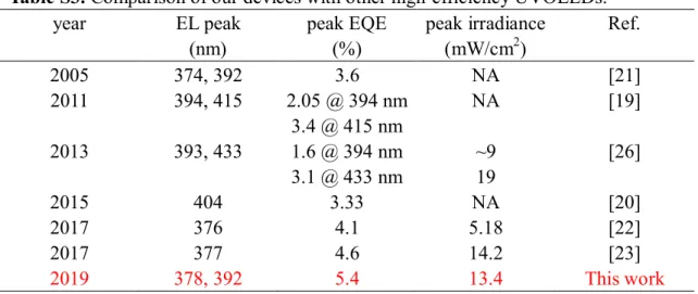
Table S3. Comparison of our devices with other high-efficiency UVOLEDs. year EL peak (nm) peak EQE (%) peak irradiance (mW/cm2) Ref. 2005 374, 392 3.6 NA [21] 2011 394, 415 2.05 @ 394 nm 3.4 @ 415 nm NA [19] 2013 393, 433 1.6 @ 394 nm 3.1 @ 433 nm ~9 19 [26] 2015 404 3.33 NA [20] 2017 376 4.1 5.18 [22] 2017 377 4.6 14.2 [23] 2019 378, 392 5.4 13.4 This work
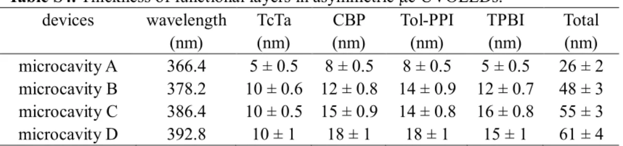
Table S4. Thickness of functional layers in asymmetric μc UVOLEDs. devices wavelength (nm) TcTa (nm) CBP (nm) Tol-PPI (nm) TPBI (nm) Total (nm) microcavity A 366.4 5 ± 0.5 8 ± 0.5 8 ± 0.5 5 ± 0.5 26 ± 2 microcavity B 378.2 10 ± 0.6 12 ± 0.8 14 ± 0.9 12 ± 0.7 48 ± 3 microcavity C 386.4 10 ± 0.5 15 ± 0.9 14 ± 0.8 16 ± 0.8 55 ± 3 microcavity D 392.8 10 ± 1 18 ± 1 18 ± 1 15 ± 1 61 ± 4
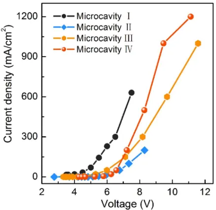
Table S5. Summary of symmetric μc UVOLEDs performances. devices peak (nm) VT (V) max. power density (mW/cm2) max. EQE (%) thickness (nm) FWHM a) (nm) microcavity I 366.2 3.50 1.88 1.44 26 ± 2 17.0 ± 1 microcavity II 378.8 2.76 2.93 2.24 48 ± 3 12.9 ± 1 microcavity III 386.0 3.32 4.26 3.48 55 ± 3 10.0 ± 0.5 microcavity IV 392.2 4.28 4.97 4.11 61 ± 4 9.95 ± 0.5 a)
FWHM: full width at half maximum.
Table S6. Comparison of our devices with other μc UVOLEDs. year tunable wavelength range (nm) FWHM (nm) peak irradiance (mW/cm2) lifetime (min) Ref. 2015 373-469 21-41 NA NA [27] 2015 370-430 24-48 1.7 NA [18] 2019 360-400 9.95-15.2 5.63 3790 This work Supporting text:
Simulation of the resonance condition and emission spectrum of microcavity
OLEDs
S- 13 -
In this equation, 1 and 2 are the phase shifts on reflection from the DBR and metal
mirror, the third term defines the phase thickness of the cavity layers; ni and di are the
refractive indices and thicknesses of the cavity layers, is the viewing angle, and m is
an integer, respectively.
According to the resonance condition, the effective cavity length is 1/2 mλ. The
determination of wavelength λ0 of a microcavity for normal incidence was also
expressed by: 2 0 1 2 2 i i pen pen i i n d L L m
(2)Where, the first term of equation defines the optical thickness of cavity layers
between two mirrors, Lpen1 and Lpen2 are penetration depths of the respective
mirrors, ni and di are the refractive indices and thicknesses of the cavity layers, is
the viewing angle, mi is the mode index.
The phase change 1 of the DBR is obtained by simulating of a multilayer dielectric
structure, whereas the phase change 2 of the metal mirror in the normal direction can
be expressed by3 2 2 2 2
2
arctan(
s m)
m m sn k
n
k
n
(3)In this equation, ns is the refractive index of the film next to the metal electrode, and
nm and km are the real and imaginary parts of the refractive index of the metal.
The penetration depth of DBR is given as 3
0 1
4
DBRL
(4)
0 24
metalL
(5)According to a model based on dipole radiation in a multilayer thin-film structure, the
emission spectrum of the microcavity OLEDs can be simulated by the traditional
optical method 3: 2 0 2 0 0 0 4 (1 ) 1 2 cos( ) ( ) ( ) 4 1 2 cos( ) d m m cav n m d m d z R R R E E L R R R R (6)
Here, Rd and Rm are the reflectances of the DBR and metal, respectively, z is the
optical distance of the emitting dipoles from the metallic mirror, L is the total optical
thickness, and En (λ0) is the EL intensity at λ0 in free space.
References
(1) Meng, Y.; Xie, W.; Xie, G.; Zhang, L.; Zhao, Y.; Hou, J.; Liu, S. Highly Efficient Blue Top-Emitting Device with Phase-Shift Adjustment Layer. Opt. Express2009, 17, 5364–5372.
(2) Ma, F.; Liu, X. Phase Shift and Penetration Depth of Metal Mirrors in a Microcavity Structure. Appl. Opt. 2007, 46, 6247–6250.
Ma, F.; Liu, X. Phase Shift and Penetration Depth of Metal Mirrors in a Microcavity Structure. Appl. Opt.2007, 46 (25), 6247–6250.
(3) Dodabalapur, A.; Rothberg, L. J.; Jordan, R. H.; Miller, T. M.; Slusher, R. E.; Phillips, J. M. Physics and Applications of Organic Microcavity Light Emitting Diodes. J. Appl. Phys.1996, 80, 6954–6964.