Grounded Capacitors
Chun-Ming Chang, Bashir M. Al-Hashimi, Yichuang Sun, and J. Neil Ross
Abstract—Despite the wealth of literature on operational transconductance amplifier (OTA)-C filters, the synthesis of high-order filter characteristics is still an active topic. In this paper the realization of voltage transfer functions based on canonical current-mode follow-the-leader-feedback (FLF) OTA-C structures are investigated. Two new structures are presented, which use only single-ended-input OTAs and grounded capacitors. The first structure has a single voltage input and multiple voltage outputs taken from different nodes, which enables it to provide simultaneous outputs of different filter functions. The second structure has a single voltage output and single voltage input dis-tributed to different circuit nodes for a universal realization. The authors not only propose such filter structures, but also show how analytical synthesis can be used to produce filter circuits that have less active elements than those recently reported voltage-mode structures which are based on differential-input OTAs. This represents another attractive feature from chip area, and power consumption point of view. Simulation results verifying the theo-retical analysis of the proposed filter structure are included.
Index Terms—Analog filters, analytical synthesis, operational transconductance amplifier (OTA)-C structures.
I. INTRODUCTION
O
VER the last decade or so numerous voltage-mode and current-mode high-order operational transconductance amplifier (OTA)-C filter structures have been reported [1]–[12]. Such structures have often been developed with different design criteria in mind, including reduced number of active elements, grounded capacitors, and simple design methods. In [9], different voltage-mode structures were proposed ca-pable of synthesizing th-order filters with both transmission poles and zeros. The filters employ active elements, and n grounded capacitors for canonical realizations. The active elements consist of single-ended-input OTAs, and differential-input OTAs. It was pointed out in [8] that single-ended-input OTAs should be employed in place of differential-input OTAs in the filter structure to avoid the generation of parasitic zeros due to the finite input parasitic capacitances of the differential-input OTAs. In [10], an OTA-C filter structure with single-ended-input OTAs, and only Manuscript received June 3, 2003; revised October 9, 2003 and November 13, 2003. This paper was recommended by Associate Editor A. M. Soliman.C.-M. Chang, B. M. Al-Hashimi, and J. N. Ross are with the School of Electronics and Computer Science, University of Southampton, High-field, Southampton, SO17 1BJ, U.K. (e-mail: [email protected]; [email protected]; [email protected]).
Y. Sun is with the Department of Electronic, Communication and Electrical Engineering, University of Hertfordshire, Hatfield AL10 9AB, U.K.
Digital Object Identifier 10.1109/TCSII.2004.831426
one differential-input OTA was presented, a structure that was also mentioned as a noncanonical follow-the-leader-feedback (FLF) structure in [9]. Whilst this noncanonical voltage-mode FLF structure has reduced the number of differential-input OTAs, it has increased the number of single-ended-input OTAs
from to , clearly an unsuitable solution from
com-ponent count point of view. In the literature, there have been a number of current-mode multiple loop feedback OTA-C filters using single-ended-input OTAs and grounded capacitors [1], [11], [12]. It would be very interesting to use the advantages of these current-mode filters to realize voltage transfer func-tions without increase in the component number and without use of differential input OTAs. Furthermore, the structures of [9]–[12] have one input and one output which mean that there is a different filter topology for different filtering function. In some applications, however, simultaneous outputs of different high-order filtering functions may be needed.
The aim of this paper is to present two new high-order OTA-C filter structures employing only single-ended-input OTAs, and grounded capacitors, based on the canonical current-mode FLF OTA-C filter structure [11], [12], but for the realization of voltage transfer functions. The first one is capable of providing different filtering functions lowpass (LP), highpass (HP), and bandpass (BP) from different nodes without changing the filter topology. This is achieved without increasing the number of active elements; in fact, it has the least number of active and passive elements when compared with some recently reported voltage-mode works including [9], [10]. The second one is obtained by adding a linear input distribution OTA network to the first one. Any voltage th-order transfer functions can be realized by the second one which simultaneously enjoys three main attractive criteria: the minimum components, only single-ended-input OTAs, and only grounded capacitors [8].
II. NEWOTA-C FILTERSTRUCTURE FORREALIZING TH-ORDER LP, BP, AND HP FILTERS OF
VOLTAGETRANSFERFUNCTION
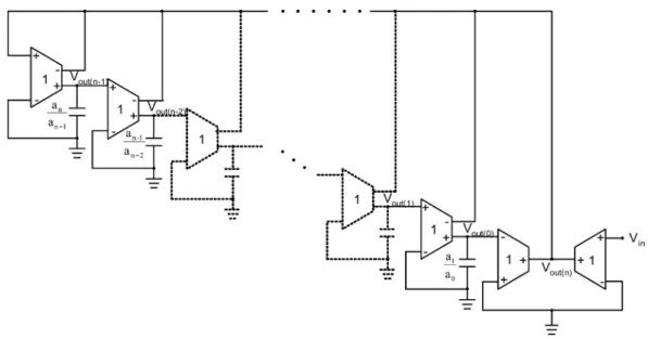
Fig. 1 shows the proposed th-order filter structure where is the filter input voltage, and
and are the filter voltage
outputs. The settings of the filter output voltages deter-mine the filter functions (LP, HP, BP). It can be seen that the structure employs only single-ended-input OTAs and grounded capacitors, an advantage of the current-mode FLF structure 1057-7130/04$20.00 © 2004 IEEE
Fig. 1. Nth-order OTA-C filter structure of the proposed analytical synthesis method.
[11], [12], which is here taken for realization of voltage transfer functions.
The filter structure of Fig. 1 is obtained as follows. The transfer functions of an th-order filter with LP, BP, and HP responses at different outputs can be written as
for where
(1) Cross multiplying the transfer function of (1) as , and rearranging the result, we obtain
(2)
From (1), we have
(3)
(4) Substituting (4) into (2) gives
(5)
Equation (5) is a voltage relationship. In order to be consistent with the input-and-output current relationship of an OTA, i.e.,
, we multiply each side of (5) by an equal transconductance of unity value (1), leading to
(6) Then, (3) can be derived as
namely
(7) Substituting (7) into (6) yields
(8) By using the active element OTA, whose characteristic
relation-ship is , and the grounded capacitor, whose
ad-mittance is , to implement (7), a fundamental OTA-grounded capacitor structure is obtained by a grounded capacitor (with ca-pacitance ) connected with the output terminal of a single-ended-input OTA (with transconductance unity) having
an input voltage and an output voltage across
the grounded capacitor. Next, we implement (8) using the output currents of the OTAs and Kirchhoff’s current law. The combi-nation of the individual circuit yields the circuit shown in Fig. 1, in which all the coefficient values are normalized.
In summary, the proposed synthesis method has decomposed the th-order transfer function (1) into transfer func-tions including first-order transfer functions [(7)] and one straint equation [(8)]. To illustrate the synthesis method,
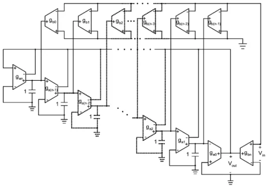
con-Fig. 2. OTA-C filter structure II for realizing generalnth-order transfer functions. sider the structure generation of a fourth-order filter. The syn-thesis method uses (7) and (8). Based on these equations, when , the fourth-order OTA-C filter has the following three transfer functions: LP BP HP where (9) It should be noted that, in general, a voltage follower may be necessary at the output of the filter to buffer the output and avoid the effects of load capacitance or resistance changing the re-sponse of the filter.
III. NEWOTA-C FILTERSTRUCTURE FORREALIZING -TH-ORDERUNIVERSALVOLTAGETRANSFERFUNCTIONS In Section II, we proposed a new filter structure, shown in Fig. 1, for realizing th-order OTA-C LP, BP, and HP filters. Equation (1), corresponding to Fig. 1, shows that there are different-order transfer functions which can be realized at different nodes in Fig. 1, respectively. The general th-order voltage transfer function
(10)
is the linear combination of the different-order transfer functions shown in (1), i.e.,
where
(11) Two synthesis approaches to realize the above relationship are proposed as follows.
i) Using the linear combination method to perform the syn-thesis, multiply both sides of (11) by and obtain
(12) Then, we take each nodal voltage in the circuit
struc-ture of Fig. 1, i.e., in which
, and , as the input voltage of an extra OTA with the transconductance . Join all
of the output terminals of the extra OTAs and
connect the summing point with an equivalent grounded resistor realized by a single-ended-input OTA with unity transconductance. The realized circuit structure uses single-ended-input OTAs and n grounded capaci-tors.
ii) A more effective synthesis approach is explained as fol-lows. Multiply both sides of (11) by and obtain the following other form [different from (12)]
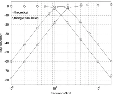
Fig. 3. Amplitude-frequency response of third-order LP and HP filters.
The physical meaning of the above relationship is “to insert different weights of the input voltage signal into each node in the filter structure shown in Fig. 1 and then obtain the output voltage signal”. According to this approach [1], [9], [12], giving a forward signal, with a weight of input voltage signal, from input voltage node to each inner node in the filter structure shown in Fig. 1, we obtain the other new OTA-C filter structure, shown in Fig. 2, for realizing the general nth-order voltage transfer function shown in (10). The realized circuit structure uses single-ended-input OTAs and n grounded capaci-tors.
The circuit structure (Fig. 2) of approach (ii) uses two fewer single-ended-input OTAs than that (Fig. 3) of approach (i) and is recommended to realize the general nth-order voltage transfer function shown in (10). Note that, in Fig. 2, all OTAs have single-ended input and all n capacitors are grounded. The num-bers of active OTAs and grounded capacitors are the minimum numbers [9] to realize such a general nth-order voltage transfer function shown in (10).
In Fig. 1, although we let all the tranconductances of the OTAs be unity and let the capacitances of n grounded capacitors be
, and , in fact, all
the values of the transconductances and the capacitances can be given flexibly. The restriction of the values of the transconduc-tances and the capacitransconduc-tances shown in Fig. 1 is used for being consistent with the derivation process and the original given transfer functions shown in (1). Similarly, in order to simplify and clarify the network analysis of Fig. 2, we let the value of each grounded capacitor be unity although, as a matter of fact, it can be given by any different required value. Circuit analysis
yields the transfer function of Fig. 2, shown in (14) at the bottom
of the page. All , can be found
ex-actly, i.e.,
and
for (15)
by solving the following equations:
(16)
All can be found exactly by solving
the following equations:
(17)
In any case, if the calculated , then, the corresponding OTA should be eliminated; and if the calculated neg-ative value, then the two input terminals of the corresponding OTA should be interchanged.
The relative sensitivities are the
values of filter characteristic parameters with respect to circuit elements. If we let the values of all capacitors from the right
side in Fig. 2 be , and , respectively,
as we divide both numerator and denominator of its transfer
function by , the transfer function of
Fig. 2 is similar to (14) by replacing with for , and . Due to space limitation, only key sensitivity results are quoted without derivation. For ex-ample, the denominator coefficient sensitivities to where , are 1 or 0. The numerator coefficient sensitivities to are
for for
for (18)
Detailed numerator and denominator coefficient sensitivities
with respect to , and are in the range from to 1
provided that all and are positive.
IV. COMPARISON WITHPREVIOUSSTUDIES ANDSIMULATIONRESULTS
Table I shows a comparison in terms of number of OTAs and types of OTAs between the proposed filter structures (Figs. 1 and 2), and those recently reported in [9] and [10].
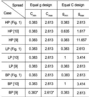
Another parameter which needs to be compared with one an-other is the span (or spread) of filter component values which may be large for high-order filters. A wider span of filter com-ponent values leads to a worse implementation carried out in CMOS which will create the quadratic current ratios. To give in-sight into what the component spread of the new filter structure shown in Fig. 1, Table II provides the comparison of the fourth-order Butterworth HP, LP, and BP filters designed using the pro-posed filter (Fig. 1) and those reported in [9], [10]. Table II gives the component spread for equal transconductance and equal capacitance designs. It can be seen that the proposed filter has the same component spread (equal design) as those in [9], [10] except the case for BP in [9]. In the case of equal design, the filter in [10] has the least component spread, and our filter has better component spread than that in [9].
To verify the theoretical analysis of the proposed filter struc-ture shown in Fig. 1, a third-order LP and HP OTA-C filter has been simulated using H-Spice with the UMC05 level-49
param-eters, with for nMOS and for pMOS
transistors, and the component values: 1) S
( A), 18 pF, 9 pF, and 4.5 pF
for the responses with 0.990 MHz, using 2.5 V,
and 2.5 V; 2) S ( 10.495 A),
10 pF, 5 pF, and 2.5 pF for the responses
with 1.999 MHz, using 2.5 V, and 2.5
V. The OTAs were implemented using the CMOS circuit given in [13]. Fig. 3 shows the simulated LP and HP responses of the filter. As can be seen, there is a close agreement between theory and simulation, for example, the simulated 3 dB frequencies are 0.94 MHz (HP) and 1.04 MHz (LP), compared to 0.990 MHz in the ideal case, and 1.83 MHz (HP) and 2.02 MHz (LP), com-pared to 1.999 MHz in the ideal case. Other filters with different
order and responses were also simulated and found to perform as theory predictions.
V. CONCLUSION
This paper has presented two new high-order filter structures (shown in Figs. 1 and 2) that employ only single-ended-input OTAs and grounded capacitors. It has been shown how decom-posing analytically an nth-order transfer function into simple realisable transfer functions using OTA-C circuits pro-duces the first filter structure that employs less active elements than some of the recently reported methods and offers simul-taneous multiple outputs. The proposed first filter structure has single-ended-input OTA, and grounded capacitors for a given filter order, . Realizing the general transfer function by using the more effective synthesis approach different from the linear combination of each output signal of the first filter structure leads to the second filter structure which can realize any kind of voltage transfer functions employing the minimum components, only “single-ended-input” OTAs, and only
“grounded” capacitors.
ACKNOWLEDGMENT
The authors would like to thank the anonymous reviewers for their constructive comments.
REFERENCES
[1] T. Deliyannis, Y. Sun, and J. K. Fidler,Continuous-Time Active Filter Design. Boca Raton, FL: CRC, 1999.
[2] M. A. Tan and R. Schaumann, “Simulating general-parameter LC-ladder filters for monolithic realizations with only transconductance elements and grounded capacitors,” IEEE Trans. Circuits Syst., vol. 36, pp. 299–307, Feb. 1989.
[3] P. V. A. Mohan, “Novel OTA-C filter structures using grounded capaci-tors,” inProc. IEEE Int. Symp. Circuits Systems, 1991, pp. 1347–1350.
[4] Y. Sun and J. K. Fidler, “OTA-C realization of general high-order transfer functions,” Electron. Lett., vol. 29, no. 12, pp. 1057–1058, 1993.
[5] Y. S. Hwang, S. I. Liu, D. S. Wu, and Y. P. Wu, “Table-based linear transformation filters using OTA-C techniques,”Electron. Lett., vol. 30, no. 24, pp. 2021–2022, 1994.
[6] R. Schaumann, “Simulating lossless ladders with transconductance cir-cuits,”IEEE Trans. Circuits Syst. II, vol. 45, pp. 407–410, Mar. 1998. [7] Y. Sun, “OTA-C filter design using inductor substitution and Bruton
transformation methods,”Electron. Lett., vol. 34, no. 22, pp. 2082–2083, 1998.
[8] Y. Sun and J. K. Fidler, “Synthesis and performance analysis of uni-versal minimum component integrator-based IFLF OTA-grounded ca-pacitor filter,” inProc. IEE Circuits Devices Syst., vol. 143, 1996, pp. 107–114.
[9] , “Structure generation and design of multiple loop feedback OTA-grounded capacitor filters,”IEEE Trans. Circuits Syst. I, vol. 44, pp. 1–11, Jan. 1997.
[10] C. A. Barbargires, “Explicit design of general high-order FLF OTA-C filters,”Electron. Lett., vol. 35, no. 16, pp. 1289–1290, 1999. [11] Y. Sun and J. K. Fidler, “Current-mode multiple-loop feedback filters
using dual-output OTAs and grounded capacitors,”Int. J. Circuit Theory Applicat., vol. 25, pp. 69–80, 1997.
[12] , “Current-mode OTA-C realization of arbitrary filter characteris-tics,”Electron. Lett., vol. 32, no. 13, pp. 1181–1182, 1996.
[13] S. Szczepanski, A. Wyszynski, and R. Schaumann, “Highly linear voltage-controlled CMOS transconductors,”IEEE Trans. Circuits Syst. I, vol. 40, pp. 258–262, Apr. 1993.