WORD LEVEL FINITE FIELD MULTIPLIERS USING
NORMAL BASIS
1B.SARGUNAM, 2Dr.R.DHANASEKARAN
1
Assistant Professor, Department of ECE, Avinashilingam University, Coimbatore 2
Professor & Director-Research, Department of EEE, Syed Ammal Engineering College, Ramanathapuram
E-mail: [email protected] , [email protected]
ABSTRACT
Finite field multipliers are widely used in elliptic curve cryptography as a basic building block. Normal basis is the most suitable for representation of binary field elements since squaring operation can be done by simple cyclic shift of its binary digits. In this paper, efficient word level multipliers using normal basis and reordered normal basis in Galois field is proposed, where Reordered Normal Basis (RNB) is referred to as certain permutation of optimal normal basis type- II. These architectures provide a better area and power efficiency when compared to the existing Word Level finite field multiplier using Normal Basis (WLNB) and Reordered Normal Basis (WLRNB). WLNB and WLRNB are coded in VHDL and simulated in Modelsim10.0b. Area and Power reports are obtained using Xilinx ISE 9.1i.
Keywords: Finite Field Multiplier, Normal Basis, Reordered Normal Basis, Cryptography,Galois Field
1. INTRODUCTION
Finite field (Galois Field (GF) (2m))
contains finite number of elements, where m is the
dimension of the field. Finite field arithmetic has many applications such as error control coding, cryptography [1, 2], public key cryptography [3,4]. In these applications, there is a need to design low complexity finite field arithmetic units. The complexity mainly depends on representation of field elements. The most commonly used basis includes polynomial basis (PB) [5, 6], normal basis (NB)[7], and dual basis (DB)[8]. Normal Basis is attractive when performing exponentiation and squaring operations [9]. The major advantage of Normal Basis is squaring operation and it can be done by simple right cyclic shift of its binary digits and it is suitable for hardware implementation. Massey and Omura were the first to propose multipliers on Normal Basis [10, 11]. The normal basis for which the complexity is minimized is referred to as optimal normal basis (ONB). Two types of optimal normal basis have been found which are referred to as optimal normal basis (ONB) types I and II [12]. Reordered normal basis is a reordered version of optimal normal basis type II and was initially proposed in [13].
Hardware implementation of finite field multipliers can be classified into three categories. First category are bit level multipliers. A bit level
multiplier takes m clock cycles to finish one
multiplication in a field of size m. The multipliers
in this class are considered to be low power consuming and taking small area of silicon. Their main disadvantage is their low multiplication speed for large field sizes. The second category is full parallel multipliers. A full parallel multiplier takes one clock cycle to finish the multiplication for any field size. These multipliers are impractical since they require large silicon area. The third category is
word level finite field multiplier which takes d
clock cycles, 1 ≤ d ≤ m, to finish one multiplication
operation of size m. The value of d can be selected
by designer to set the tradeoff between area and
speed. Decreasing the value of d will result in faster
and larger multipliers while increasing d will make
smaller multipliers. The extensive use of Normal basis in exponentiation and more practical significance of word level together attract the researchers to work in this area.
Two normal basis multipliers which are compared here are word level finite field multiplier using normal basis and word level finite field multiplier using re-ordered normal basis. Sequential
multiplier produce one bit for every m clock cycle.
Such multipliers are referred to as SMSO (Sequential Multiplier with Serial Output). The
sequential multipliers which generate all m bits of
the product at m-1 cycle and further become the
final product at end of the mth cycle are referred to
word level finite field multiplier using normal basis.
In this paper, a word level normal basis multiplier using NAND gate is proposed. When the AND gates in the WL-NB scheme is replaced by NAND gates, this proposed multiplier has a smaller number of gates .This modification gives a better area when compared to the previous similar proposals. An efficient word level multiplier using reordered normal basis is designed. This multiplier helps in reducing the number of clock cycles for multiplication operation. It is shown that the new design has lower number of gates and efficient power consumption comparing to other similar proposals.
The rest of the paper is as follows: Preliminaries of Normal Basis and Reordered Normal Basis are reviewed in section 2. A word level NB algorithm and its architecture are discussed in section 3. A word level multiplier using Reordered Normal Basis is presented in section 4. Simulation results are given in 5. Complexity comparisons are made in section 6. Conclusion is given in section 7.
2. PRELIMINARIES
In this section Normal basis representation and Reordered Normal basis definition are illustrated.
2.1 Normal Basis Representation
It is well known that there always exists a
normal basis in the field GF (2m) over GF (2) for all
positive integers m in [1], [15]. By finding an
element β ∈ GF(2m) such that
{β, β2,…… β2^(m-1)
} (1)
is a basis of GF(2m) over GF(2).Then element A ∈
GF(2m) can be represented as
A ∑ ai β2^i = a0β + a1β2 + … + am-1 β2^(m-1) (2)
Where ai GF(2m), 0 i m-1, is the ith
coordinate of A with respect to the NB. In short, the normal basis representation of A will be written as A = (a0,a1,……..am-1) (3)
The main advantage of the NB representation is that an element A can be easily squared by applying right cyclic shift of its coordinates, since
A2 = (am-1, a0,….,am-2)
= am-1β + a0β
2
+... +am-2β
2^(m-1).
2.2 Reordered Normal Basis Definition
Let β be a primitive (2m+1)st root of unity in F2m (β2m+1 = 1) and γ = β +β-1 generates a type II
optimal normal basis. Then {γi,i = 1,2,…,m} with
γi = βi + β-i = βi + β2m+1-i, i = 1,2,…,m, is also a basis in F2m. It has been shown that the basis { γi , i =
1,2,….,m} is a permutation of the normal basis {
γ2^i,i = 0,1,....,m-1 }. We denote the basis I2 = { γ1,
γ2,….,γm} as the reordered normal basis following
[14].
Reordered normal basis not only offers free squaring but also avoid modulo reduction step in a multiplication operation.
3
.
WORD LEVEL NB MULTIPLICATIONALGORITHM
Let the field elements A, B GF (2m) are
represented using NB. Let the word size be w, 1 ≤
w ≤ m and d = [m/w], where d is the number of clock cycles.
Algorithm: Word level NB multiplication [16]
Input: ai, bi, i = 0, 1,…., m-1, also let bi = 0 for m ≤ i ≤ dw-1.
Output: ck, k = 0, 1,…., m-1
1. INTIALIZATION: r = 0, k = 0, 1,…., m-1.
2. FOR l := 1 TO d STEP 1 DO
3. FOR ALL VALUES OF k = 0, 1……, m-1 DO
IN PARALLEL
4.
r ≔
r
∑ b∑ at ,
The final value
r = ck for k = 0, 1,….., m-1
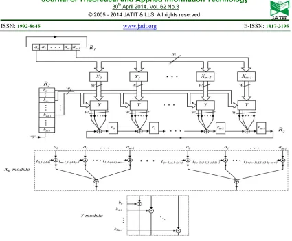
According to the algorithm, word level multiplier can be designed as shown in figure 1[16]. The above architecture contains three shift registers R1, R2, R3 respectively. R1 is the m bit shift register which contains the coefficient of operand A, where m is a number of bits. R2 acts as an m bit shift register initially with the coefficients of operand B and takes “0” bit after every clock cycle as its input.
Register R3 is an m 1-bit registers which are serially
connected by XOR gates. Finally the output will be stored in the Register R3.There are m pairs of Xk and Y modules are working in parallel.
The architecture takes d clock cycles to
complete one multiplication operation where the value of d, 1 ≤ d ≤ m, can be selected by the designer to set the tradeoff between Area and
XOR networks and has an output of w bits. A
corresponding Y module is made out of w two input
AND gates and generating the w product bits of w
coefficients of operand A, and w output bits of Xk module. The last set of register in the architecture
R3 which are serially connected by XOR gates, are
implementing the exclusive OR and shift operations. The accumulation operation can be
performed with the shift register R3.The output can
be concatenated in a separate variable.
The architecture of word level multiplier in finite field using normal basis designed in the
example is shown in figure 2, where m=5, w=2, and
d=3. A multiplication operation in finite field can
be implemented using one AND gate while an addition operation can be implemented using one
XOR gate. This multiplier takes d = 3 clock cycles
to compute the product bits. During the first clock cycle, register R1 rotate right cyclic shift of its
binary digit and the output of the R1 are summed
with the corresponding binary digits. Register R2
loaded with ‘0’ bit for every clock cycle and multiplied with the output of XOR network to produce the partial product bit. At the end of the
third clock cycle register R3 contains the output of
the one multiplication operation.
In the architecture of word level NB multiplier, a modification is made. Instead of AND gate in the Y module, NAND gate is used in order to reduce the area and power complexity. By using NAND gate the result of the multiplication will be reversed. After that by doing XOR operation that is addition, final result will not be changed. Complexity comparison results show that the Word Level NB multiplier using NAND gate is area efficient when compared to other similar proposals. The comparison results are shown in section 7.
4. WORD LEVEL MULTIPLIER USING
RNB
The architecture of reordered normal basis multiplier is designed [17] as shown in figure 3. Operand A and operand B are two inputs which contains five bits. Operand B is reordered reversely and right cyclic shift operation for every clock cycle. The architecture contains 2m+1 bit circular shift register which should be initialized with one
of the input coefficients. The
expansion/permutation module is just reordering and copying module which doesn’t contain any gates. This module accepts 2m+1 inputs from the circular shift register and provides 2km outputs for
the two input AND gates, where k be the number of words. The two bits of operand B are first added together and then the sum multiplies one bit of operand A to produce partial product bit. The partial product bit is fed into the accumulation unit. The accumulation unit contains XOR network and flip-flop. The input of the XOR network and the output of the flip-flop are summed together to produce the output. The output can be taken from the operand C. It requires two clock cycles to produce the output. So wherever high speed multipliers are required, Reordered Normal Basis technique can be applied.
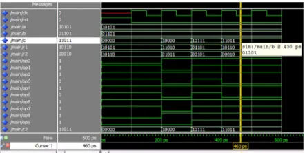
5. SIMULATION RESULTS
WL-NB, WL-NB using NAND gate and WL-RNB are coded using VHDL and simulated in MODELSIM 10.0b. Clock, reset, a, and b are the
inputs and r3 is the output. The remaining values
[image:3.595.305.523.451.573.2]shown in the figure are signals. The simulation waveform for Word level finite field multiplier using Normal Basis is shown in figure 4. The simulation waveform for Word Level finite field multiplier using Normal Basis with NAND gates is shown in figure 5. The simulation waveform for Word Level finite field multiplier using Reordered Normal Basis is shown in figure 6.
Figure 4: Simulation Waveform for WL-NB
[image:3.595.306.527.590.701.2]Figure 6: Simulation Waveform for WL-RNB
Simulations are carried out for multiplication of 5-bit normal basis data words ‘a’ and ‘b’. The structure of these 5-bit multipliers for normal basis and reordered normal basis are shown in figure 2 and figure 3 respectively.
6. COMPARISON RESULTS
The finite field multiplier is implemented in Xilinx ISE with WL-NB, WL-NB using NAND gate and WL-RNB. A table is formulated to show the results. The equivalent number of gates used in each technique is estimated and tabulated in table 1. This comparison table indicates the reduction in area. In a similar manner, the power is also estimated and compared. The comparison results for gate count that is area and power are also shown in the figure 7 and figure 8 as a graphical plot for
[image:4.595.87.520.85.407.2]better comparison.
Table 1: Gate Count and Power Comparison
Type of Multiplier
Area (Equivalent
number of gates used)
Power Usage (mW)
WL-NB 2854
38
WL-NB using NAND gate
1956
35
WL-RNB 1844 35
[image:4.595.302.511.348.524.2]Figure 7: Area Comparison
Figure 8: Power Comparison
7. CONCLUSION
In this paper, word level finite field multiplier using Normal Basis, Normal Basis with NAND gate and Reordered Normal Basis are presented.
Architectural complexity comparison and
numerical examples show that the architecture using Reordered Normal Basis is faster and performs better compared to other similar proposals considering area and power as a measure of performance. The Word Level multiplier using Reordered Normal Basis can be used for public key cryptography applications where high speed multipliers are required. The Reordered Normal Basis Multiplier also can be modified using NAND gates and the complexity will be reduced further. The normal basis multiplier is more effective in
0 500 1000 1500 2000 2500 3000
WL-NB WL-NB
using NAND gate
WL-RNB
Area (Gate Count)
33 34 35 36 37 38
WL-NB WL-NB
using NAND gate
WL-RNB
[image:4.595.95.284.520.697.2]finding inverse or squaring or exponentiation of the finite field element. However, in case of multiplier the order of the field goes up, the area of normal basis multiplier increases dramatically. This finds the limitations in the use of normal basis multiplier in high order finite field applications.
REFERENCES:
[1] Erkay Savas¸ and Çetin Kaya Koç,”Finite Field Arithmetic for Cryptography” Math. Computation, vol. 64, no. 2, pp. 1227-1233, 1995.
[2] D. Hankerson, A. Menezes, and S. Vanstone, “Guide to Elliptic Curve Cryptography”, Springer,
http://www.cacr.math.uwaterloo.ca/ecc/, Dec. 2003.
[3] IEEE Std 1363-2000, IEEE Standard
Specifications for Public-Key Cryptography, Jan. 2000.
[4] T. Beth and Gollman, “Algorithm
Engineering for Public Key Algorithms,” IEEE J. Selected Areas in Comm., vol. 7, no. 4, pp. 458- 465, May 1989.
[5] I.S.Hsu, T.K.Truong, H.M.Shao,and
L.J.Deutsch, “A comparison of VLSI
architecture of Finite Field Multipliers using
Dual, Normal or Standard basis” IEEE
Transaction. Computers, vol. 37, no. 6, pp. 735-739, June 1988.
[6] Che-Wun Chiou and Huey-Lin Jeng,”Parallel algorithm for polynomial basis multiplier in
GF(2m) Fields”, Tamkang Journal of Science
and Engineering, Vol. 11, No. 2, pp. 211-218 (2008).
[7] A. Reyhani-Masoleh and M.A. Hasan,
“Efficient Digit-Serial Normal Basis
Multipliers over GF (2m),” proceeding of
IEEE International Symposium on Circuits and Systems, Volume: 5, 2002.
[8] Chiou-Yng lee and Jenn shyong horng,”Low complexity Bit parallel multiplier over
GF(2m) using dual basis representation”,
Journal of Computer Science and Technology, Vol.21, no.6, pp.887-892, Nov. 2006.
[9] A. H. Namin, H. Wu and M. Ahmadi, “High Speed Word-parallel Bit-Serial Normal Basis Finite Field Multiplier and Its FPGA
Implementation”, Proceedings of the 39th
Asilomar Conference on Signals, Systems, and Computers, pp. 1338-1341, Nov. 2005. [10] J.L. Massey and J.K. Omura, “Computational
Method and Apparatus for Finite Field Arithmetic,” US Patent Application, 1984. [11] C.K. Koc and B. Sunar, “Low-Complexity
Bit- Parallel Canonical and Normal Basis
Multipliers for Class of Finite Fields,” IEEE
Transaction Computers, vol. 47, no. 3, pp. 353-356, Mar. 1998.
[12] R.C.Mullin and R.M Wilson, “Optimal
Normal bases In GF(pn)”, Discrete Applied
Mathematics, vol. 22, pp. 149-161, 1989. [13] S. Gao and S. Vanstone, “On order of optimal
normal basis generators,” Math. Comp., vol.
64, No. 2, pp. 1227-1233,1995.
[14] Huapeng Wu, M. Anwarul Hasan, Ian F. Blake, Shuhong Gao, “Finite Field Multiplier Using Redundant Representation”, IEEE Trans. Computers 51(11): 1306-1316 (2002). [15] A. Reyhani-Masoleh and M.A. Hasan, “Low
Complexity Word-Level Sequential Normal Basis Multipliers,” IEEE Trans. Computers, vol. 54, no. 2, pp. 98-110, Feb. 2005.
[16] Ashkan Hosseinzadeh Namin, Huapeng Wu, and Majid Ahmadi,” A Word-Level Finite Field Multiplier Using Normal Basis”, IEEE transactions on computers, Vol. 60, no. 6, pp. 890-895, June 2011.
[17] Ashkan Hosseinzadeh Namin , Huapeng Wu
and Majid Ahmadi,, “High Speed
architectures for Multiplication using
Figure 1: Architecture of Word Level Multiplier in Finite Field using Normal Basis
[image:6.595.93.488.468.714.2]