N A N O E X P R E S S
Open Access
Optical properties and bandgap evolution of ALD
HfSiO
x
films
Wen Yang
1, Michael Fronk
2, Yang Geng
1, Lin Chen
1*, Qing-Qing Sun
1*, Ovidiu D Gordan
2, Peng zhou
1,
Dietrich RT Zahn
2and David Wei Zhang
1Abstract
Hafnium silicate films with pure HfO2and SiO2samples as references were fabricated by atomic layer deposition (ALD) in this work. The optical properties of the films as a function of the film composition were measured by vacuum ultraviolet (VUV) ellipsometer in the energy range of 0.6 to 8.5 eV, and they were investigated systematically based on the Gaussian dispersion model. Experimental results show that optical constants and bandgap of the hafnium silicate films can be tuned by the film composition, and a nonlinear change behavior of bandgap with SiO2 fraction was observed. This phenomenon mainly originates from the intermixture ofd-state electrons in HfO2and Si-O antibonding states in SiO2.
Keywords:HfSiOx; VUV; Bandgap
Background
With the downscaling of CMOS devices, high-k mate-rials are required to replace SiO2 as gate dielectrics in
order to decrease the direct tunneling leakage current and, at the same time, maintain the gate capacitance at a certain value [1-7]. Among the potential candidates, haf-nium silicate was chosen as the first generation of
high-kdielectrics for its high dielectric constant and excellent thermal stability [8,9]. Compared to other deposition methods used for hafnium silicate film fabrication, ato-mic layer deposition (ALD) has the advantages of precise film thickness and stoichiometry control, which are of great significance to optimize the material especially for the shrinking devices [10-15].
Since accurate determination of the optical properties is an essential prerequisite for device simulations and gives the opportunity to improve material preparation, we have applied vacuum ultraviolet (VUV) spectroscopic ellipsometry to investigate the optical characteristics of a set of hafnium silicate films in this work. It will also gain us an insight into the effect of film composition on the electrical performance and chemical states of hafnium silicate dielectric films.
Methods
The targeted HfSiOxthin films were deposited on lightly
doped p-type Si (100) substrates by a BENEQ TFS-200 ALD system (BENEQ Oy, Espoo, Finland) at 200°C. The Si wafers were cleaned via RCA cleaning process at first, then prior to film growth, they were cleaned again in a diluted HF solution (50:1) to remove the native oxide and passivate the silicon dangling bonds followed by a de-ionized water rinsing and drying in N2. During deposition
process, precursors for Hf, Si, and O were TEMAH, TDMAS, and O2plasma respectively. TEMAH was kept
at 80°C in a stainless bottle, and TDMAS was kept at room temperature. The O2 plasma was activated at the
power of 100 W. Typical pulsing sequences during the ALD process are 1/3/2/2 s (TEMAH/Ar purge/O2plasma/
Ar purge) and 2/2/2/2 s (TDMAS/Ar purge/O2plasma/Ar
purge) for the growth of HfO2and SiO2films, respectively.
For the HfSiOx films, SiO2percentage was controlled by
deposition cycle ration of HfO2: SiO2. Pure HfO2, SiO2,
and five groups of HfSiOx samples with different atomic
compositions were prepared.
For optical characterization, each sample was measured using a Woollam variable-angle vacuum ultraviolet spec-troscopic ellipsometer (SE), and the data were analyzed with the software Complete EASE by J.A. Woollam. The measurements were taken at two angles of incidence, 67.5° and 75°, with a spectroscopic range of 0.6 to 8.5 eV. * Correspondence:[email protected];[email protected]
1
Institute of Advanced Nanodevices, School of Microelectronics, Fudan University, No. 220 Handan Road, Shanghai 200433, China
Full list of author information is available at the end of the article
Then, to determine the optical properties of the target samples, such as layer thickness and optical constants, the model-based analysis were carried out. Complete EASE includes a wide range of built-in functions, such as Lorentz, Gaussian, Drude, Tauc-Lorentz, and Cody-Lorentz. These functions can be used to approach a wide variety of thin film, ranging from dielectrics and organics to semiconductors and metals. In this work, the Cauchy dispersion relation was adopted for the determination of the films thickness and the optical properties were ana-lyzed with the Gaussian dispersion model.
Results and discussion
The low energy range of each spectrum (0.6 to 4 eV) was used to determine the thickness of the sample by Cauchy dispersion relation, which is often adopted to describe the refractive index for transparent films in the visible spectral range. The Cauchy formula can be given bynð Þ ¼λ Aþ B
λ2þλC4. The extinction coefficientkequals 0 at all used wavelengths. In this equation, the‘A’ param-eter relates to the approximate amplitude for the mater-ial index, while‘B’and‘C’parameters provide the shape and curvature of the index versus wavelength. Film thicknesses of each sample obtained from Cauchy dis-persion relation are listed in Table 1 (in the table HfSiOx
films are denoted as (HfO2)1-x(SiO2)x, where x refers
to different Si concentrations) together with the MSE values. ‘MSE’ is an acronym for mean squared error. It is the metric used to quantify the agreement be-tween the experimental data and the parameterized optical model. ‘Perfect’ agreement would yield a MSE value equal to 0, and large deviations away from 0 will lead to erroneous extracted physical values (i.e., thick-ness and optical constants) [16,17]. From Table 1, it can be seen that for all samples, MSEs are very small values, and error bar of each sample is at least 2 magni-tudes smaller than the thickness obtained, proving the correctness of extracted thickness.
To analyze the optical properties (behavior of refractive index and extinction coefficient), film thickness acquired
above were fixed and Gaussian dispersion model was used with the fitted range expanded to 0.6 to 8.5 eV. The Gaussian oscillator features a Gaussian line shape for the imaginary part of the complex dielectric functionε2, with
a Kramers-Kronig consistent line shape for the real part of the dielectric functionε1[18]:
εn2¼Ane−ððE−EnÞ=BrnÞþAne−ððEþEnÞ=BrnÞ ð1Þ
εn1¼ε1ð Þ þ∞ 2 πP
Z∞
Eg
ζεn2ð Þζ dζ ζ2−
E2 ð2Þ
In the equations above, the P stands for the Cauchy principal part of the integral. The Gaussian oscillator model employs four setting parameters: the amplitude
A, the broadening parameter Br, the center energy En,
and the non-dispersive term ε1(∞). The two fitting
pa-rametersBrandEnare in units of energy whileAandε1
(∞) are dimensionless.ε1(∞) represents the contribution
of the optical transitions at higher energies and appears as an additional fitting parameter [19].
As an example, the experimental SE data Ψ and Δ of HfSiOx sample with 80% SiO2 are shown in Figure 1.
[image:2.595.306.539.550.707.2]For both incidence angles, fairly good agreement be-tween the experimental and fitted spectra are clearly demonstrated, revealing that the Gaussian model works well and optical constants of the film can be exactly de-termined by the best fitting results. Data of other sam-ples are not shown here due to space limitations, but fitted data for all samples match as well with the experi-mental data.
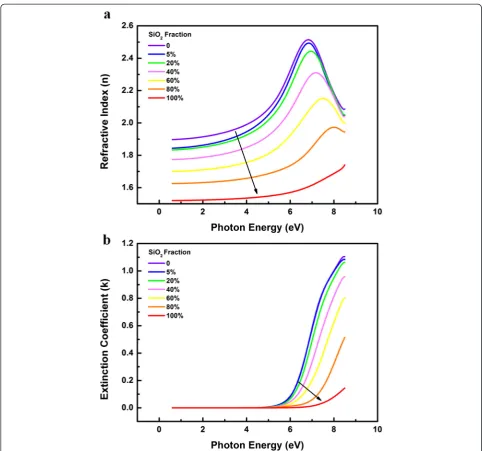
Figure 2a shows the refractive indexnas a function of photon energy for all samples as deduced from the ana-lysis of the SE results. Thenvalue for HfO2measured at
[image:2.595.55.292.614.724.2]550-nm (2.26 eV) wavelength is 1.84, which is similar with the previous report [20]. In addition, as shown in
Table 1 Thickness of samples by Cauchy dispersion relation
Thickness (nm) MSE
HfO2 9.80 ± 0.015 0.613
(HfO2)0.95(SiO2)0.05 12.00 ± 0.020 0.983
(HfO2)0.8(SiO2)0.2 10.39 ± 0.021 0.810
(HfO2)0.6(SiO2)0.4 9.36 ± 0.026 1.035
(HfO2)0.4(SiO2)0.6 8.80 ± 0.026 1.019
(HfO2)0.2(SiO2)0.8 11.36 ± 0.039 0.661
SiO2 11.13 ± 0.049 0.641
MSE = mean squared error.
Figure 2a, the index of refraction decreases with the in-crease of Si concentration in the films. According to the Lorentz-Lorenz relation [21], the refractive index can be related to the evolution of packing density and po-larization. Since Si-O bonds tend to be less polar than the corresponding Hf-O bond [22], the increase of Si concentration in the film would lead to a decrease of the film polarization, then lower polarizability results in the lowering of the refractive index.
The evolution of extinction coefficient k is shown in Figure 2b. For all samples,ksaturates to zero in the vis-ible region, suggesting the realization of high quality HfSiOx films in terms of optical properties. An abrupt
[image:3.595.56.539.86.537.2]increase in the extinction coefficient for higher photon energy is due to the fundamental bandgap absorption in the films. Moreover, as can be seen in Figure 2b, there is also a mall band tail below the gap. This weak absorp-tion is attributed to the Urbach tail which exists below the bandgap of amorphous materials and due to the dis-order of the amorphous network [23,24]. Furthermore, with the increase of Si concentration, decrease in the magnitude of the exponential tail can be observed, and similar results were obtained by the Cody-Lorentz mo-del and Tauc-Lorentz momo-del [16]. According to J. Price et al., this phenomenon is attributed to Si atoms filling the O2 vacancies/defects in the HfO2 films. By filling
these vacancies, there is less disorder and therefore, less intraband absorption.
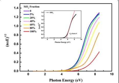
Optical bandgap of the films were determined by plot-ting the empirical expression (nαhν)1/2 versus hν, as shown in Figure 3, where n,α, and hνstand for the in-dex of refraction, the absorption coefficient, and the photon energy, respectively. The absorption coefficientα can be easily obtained by the equationα= 4πk/λ, where
λ is the wavelength of the incidence light [25]. By ex-trapolating the straight near the band edge to zero, the crossing point with thex-axis is considered to be the op-tical bandgap of the film. To make it clear, bandgap determination of HfO2 is taken as an example and is
shown in the inset of Figure 3. The extracted bandgap of pure HfO2 film is 5.64 eV, in good agreement with
[image:4.595.305.539.88.264.2]the previously reported values 5.25 to 5.8 eV for HfO2
[23,26,27].
Based on the method depicted above, the set of optical bandgaps acquired in Figure 3 is plotted in Figure 4 for details. As an exception, the bandgap of pure SiO2is not
shown in Figure 4, because although the fitted range is sufficient for most of the samples, it is not for pure SiO2
and the linear part of the curve in Figure 3 has not ap-peared yet. It is clearly demonstrated in Figure 4 that with increasing Si concentration, there is a monotonic-ally increase in the bandgap of the films. This change mainly originates from the slight difference in electro-nic structure. And if we go into details, it can be found that Eg increases rapidly when SiO2 fraction is more
than 60%. The similar nonlinear change of HfSiOx
band-gap with Si concentration was also observed by others [28,29]. It is known that the nonbonding O 2p states form the top of the SiO2 valence band and that the
Si-O antibonding states form the bottom of its con-duction band [17]. In the case of HfO2, the top of valence
band are also composed of O 2pstates but the bottom of conduction band states are mostly composed of Hf
localized 5dstate [28]. Similar to the explanation given by H. Kato et al. in the case of ZrSiOx film [29], the
rapid decrease in Eg with an increase in Hf
concentra-tion is considered to be attributed to the increase in the
d-state electrons. When Si fraction is lower than 0.6, it seems that the bottom of the conduction band is almost formed by the Hf d-states, leading to the gradual de-crease inEg.
Conclusions
The optical properties of ALD hafnium silicate films, together with pure HfO2 and SiO2 films as references,
were investigated systematically based on Gaussian dis-persion model. According to the results, optical con-stants and bandgap of the hafnium silicate films can be tuned by the film composition, and a nonlinear change behavior of bandgap with SiO2 fraction was observed.
This phenomenon mainly originates from the intermix-ture ofd-state electrons in HfO2and Si-O antibonding
states in SiO2.
Competing interests
The authors declare that they have no competing interests.
Authors’contributions
WY made physical tests, analyzed the results, and drafted the manuscript. YG carried out the manufacture of samples. MF made the optical tests and supplied valuable discussion about the analysis. LC and Q-Q S conceived of the study and participated in its design and coordination. LC, Q-Q S, ODG, PZ, DRTZ, and DWZ participated in the design of the study and helped to draft the manuscript. All authors read and approved the final manuscript.
Acknowledgements
This work was supported by the NSFC (61076114, 61106108) and Shanghai Educational Develop Foundation (10CG04), SRFDP (20100071120027), and the S&T Committee of Shanghai (1052070420).
[image:4.595.58.291.552.715.2]Figure 3Determination of the optical bandgap.
Author details
1
Institute of Advanced Nanodevices, School of Microelectronics, Fudan University, No. 220 Handan Road, Shanghai 200433, China.2Semiconductor
Physics, Technische Universität Chemnitz, Reichenhainer Straße 70, Chemnitz D-09107, Germany.
Received: 16 November 2014 Accepted: 30 December 2014
References
1. Kopani M, Mikula M, Pinčík E, Kobayashi H, Takahashi M. FT IR spectroscopy of silicon oxide and HfSiOxlayer formation. Appl Surf Sci. 2014;312:117–9.
2. Bothe KM, von Hauff PA, Afshar A, Foroughi-Abari A, Cadien KC, Barlage DW. Electrical comparison of HfO2and ZrO2gate dielectrics on GaN.
IEEE T Electron Dev. 2013;60:4119–24.
3. Hsu HW, Huang HS, Chen HW, Cheng CP, Lin KC, Chen SY, et al. Time dependent dielectric breakdown (TDDB) characteristics of metal-oxide-semiconductor capacitors with HfLaO and HfZrLaO ultra-thin gate dielectrics. Solid State Electron. 2012;77:2–6.
4. Oh J, Myoung J, Bae JS, Lim S. Etch behavior of ALD Al2O3on HfSiO
and HfSiON stacks in acidic and basic etchants. J Electrochem Soc. 2011;158:D217.
5. Cheng X, Qi Z, Zhang G, Chen Y, Li T, Pan G, et al. The interface reaction of high-k La2Hf2O7/Si thin film grown by pulsed laser deposition. Appl Surf Sci.
2009;256:838–41.
6. Dimoulas A, Vellianitis G, Mavrou G, Apostolopoulos G, Travlos A, Wiemer C, et al. La2Hf2O7high-κgate dielectric grown directly on Si(001) by
molecular-beam epitaxy. Appl Phys Lett. 2004;85:3205–7.
7. Wilk GD, Wallace RM, Anthony JM. High-κgate dielectrics: current status and materials properties considerations. J Appl Phys. 2001;89:5243–75. 8. Geng Y, Yang W, Zhu S, Zhang Y, Sun Q, Lu H, et al. Effect of ozone
treatment on the optical and electrical properties of HfSiO thin films. Appl Phy A. 2014;116:259–63.
9. Lee S, Yun D, Rhee S, Yong K. Atomic layer deposition of hafnium silicate film for high mobility pentacene thin film transistor applications. J Mater Chem. 2009;19:6857–64.
10. Gu YZ, Lu HL, Geng Y, Ye ZY, Zhang Y, Sun QQ, et al. Optical and microstructural properties of ZnO/TiO2nanolaminates prepared by atomic
layer deposition. Nanoscale Res Lett. 2013;8:107.
11. Zheng S, Sun QQ, Yang W, Zhou P, Lu HL, Zhang DW. Modulation in current density of metal/n-SiC contact by inserting Al2O3interfacial layer.
Nanoscale Res Lett. 2013;8:116.
12. Fang RC, Sun QQ, Zhou P, Yang W, Wang PF, Zhang DW. High-performance bilayer flexible resistive random access memory based on low-temperature thermal atomic layer deposition. Nanoscale Res Lett. 2013;8:92.
13. Zhou P, Ye L, Sun QQ, Wang PF, Jiang AQ, Ding SJ, et al. Effect of concurrent joule heat and charge trapping on RESET for NbAlO fabricated by atomic layer deposition. Nanoscale Res Lett. 2013;8:91.
14. Ding SJ, Chen HB, Cui XM, Chen S, Sun QQ, Zhou P, et al. Atomic layer deposition of high-density Pt nanodots on Al2O3film using (MeCp)Pt(Me)3
and O2precursors for nonvolatile memory applications. Nanoscale Res Lett.
2013;8:80.
15. Ye ZY, Lu HL, Geng Y, Gu YZ, Xie ZY, Zhang Y, et al. Structural, electrical, and optical properties of Ti-doped ZnO films fabricated by atomic layer deposition. Nanoscale Res Lett. 2013;8:108.
16. Price J, Hung PY, Rhoad T, Foran B, Diebold AC. Spectroscopic ellipsometry characterization of HfxSiyOzfilms using the Cody-Lorentz parameterized
model. Appl Phys Lett. 2004;85:1701–3.
17. Griscom DL. The electronic structure of SiO2: a review of recent
spectroscopic and theoretical advances. J Non-Cryst Solids. 1977;24:155–234. 18. Khoshman JM, Kordesch ME. Vacuum ultra-violet spectroscopic ellipsometry
study of sputtered BeZnO thin films. Optik - Int J Light Electron Opt. 2011;122:2050–4.
19. von Blanckenhagen B, Tonova D, Ullmann J. Application of the Tauc-Lorentz formulation to the interband absorption of optical coating materials. Appl Opt. 2002;41:3137–41.
20. Jerman M, Qiao ZH, Mergel D. Refractive index of thin films of SiO2, ZrO2, and
HfO2as a function of the films’mass density. Appl Opt. 2005;44:3006–12.
21. Mergel D, Buschendorf D, Eggert S, Grammes R, Samset B. Density and refractive index of TiO2films prepared by reactive evaporation. Thin Solid
Films. 2000;371:218–24.
22. He G, Zhang LD, Meng GW, Li GH, Fei GT, Wang XJ, et al. Composition dependence of electronic structure and optical properties of Hf1-xSixOygate
dielectrics. J Appl Phys. 2008;104:104116.
23. Nguyen NV, Davydov AV, Chandler-Horowitz D, Frank MM. Sub-bandgap defect states in polycrystalline hafnium oxide and their suppression by admixture of silicon. Appl Phys Lett. 2005;87:192903.
24. Ferlauto AS, Ferreira GM, Pearce JM, Wronski CR, Collins RW, Deng X, et al. Analytical model for the optical functions of amorphous semiconductors from the near-infrared to ultraviolet: Applications in thin film photovoltaics. J Appl Phys. 2002;92:2424–36.
25. Xu Y, Chen L, Sun Q, Gu J, Lu H, Wang P, et al. Electronic structure and optical properties of Nb doped Al2O3on Si by atomic layer deposition.
Solid State Commun. 2010;150:1690–2.
26. Lim S, Kriventsov S, Jackson TN, Haeni JH, Schlom DG, Balbashov AM, et al. Dielectric functions and optical bandgaps of high-K dielectrics for metal-oxide-semiconductor field-effect transistors by far ultraviolet spectroscopic ellipsometry. J Appl Phys. 2002;91:4500–5.
27. Afanas Ev VV, Stesmans A, Tsai W. Determination of interface energy band diagram between (100)Si and mixed Al–Hf oxides using internal electron photoemission. Appl Phys Lett. 2003;82:245–7.
28. Jin H, Oh SK, Kang HJ, Cho MH. Band gap and band offsets for ultrathin (HfO2)x(SiO2)1−xdielectric films on Si (100). Appl Phys Lett. 2006;89:122901.
29. Kato H, Nango T, Miyagawa T, Katagiri T, Seol KS, Ohki Y. Plasma-enhanced chemical vapor deposition and characterization of high-permittivity hafnium and zirconium silicate films. J Appl Phys. 2002;92:1106–11.
Submit your manuscript to a
journal and benefi t from:
7Convenient online submission
7Rigorous peer review
7Immediate publication on acceptance
7Open access: articles freely available online
7High visibility within the fi eld
7Retaining the copyright to your article