N A N O E X P R E S S
Open Access
Multi-functional Device with Switchable
Functions of Absorption and Polarization
Conversion at Terahertz Range
Lin Peng
1,2*, Xing Jiang
1and Si-min Li
1,3Abstract
Terahertz electromagnetic (EM) wave components usually have a single function, such as they can only convert the polarization state of an incident wave or absorb the incident energy, which would be a limitation for their applications. To make a breakthrough, a multi-functional device (MFD) is proposed in this paper, and it is capable of switching between absorption mode and polarization conversion mode. The device has a low-profile and simple structure, and it is constructed by graphene-based absorbing metasurface (AM) and gold-based polarization conversion metasurface (PCM). By controlling the chemical potential (μc) of the graphene, the leading role is transferred between the AM and the PCM, which leads to steerable absorption and polarization conversion (PC) modes. For the PC mode, the simulated polarization conversion ratio (PCR) is larger than 0.9 in the 2.11–3.63-THz band (53.0% at 2.87 THz). For the absorption mode, the simulated absorptivity is larger than 80% in the 1.59–4.54-THz band (96.4% at 3.06 THz). The physical mechanisms and operating characteristics of the MFD are discussed. This research has potential applications in terahertz imaging, sensors, photodetectors, and modulators.
Keywords:Absorption mode, Polarization conversion mode, Terahertz, Graphene, Metasurface
Introduction
Absorbers and polarization converters, capable of regulating electromagnetic (EM) wave, are two crucial devices for terahertz technology. They have significant applications in sensors, photodetectors, and modulators, and they are indis-pensable in medical imaging/diagnostics, environmental monitoring and surveillance, chemical spectroscopy, high-resolution radar, and high-speed communication [1–4]. The absorbers are utilized to absorb and dissipate the impinging EM wave, while the polarization converters have the capacity of polarization state regulating of the illumin-ating wave. These devices are widely studied in recent years [4–24].
Metasurfaces are found to have perfect absorption in the terahertz wave range [5–8]. This metasurface can be constructed by gold patterns or graphene patterns. The
gold patterns include coupled ring resonator and cross-shaped structure [5], cross-shaped gold resonator [6], and three-layer cross-shaped gold resonators [9]. However, the bandwidths of these gold metasurface absorbers are quite narrow. Graphene, which supports surface plasmons in the terahertz range [10,11], is a good material to design metasurface-based absorber with a wide bandwidth. The fishnet graphene pattern achieves a bandwidth of 59.4% at 3.2 THz [12], the dual-ring structure with hybridized plas-monic resonances obtains a bandwidth of 1.18–1.64 THz (32.6%) [13], the nine layers of different size graphene ribbons realizes good absorption from 3 to 7.8 THz (88.9%) [14], and the three-layer asymmetrically pattern graphene strips etched with holes in [15] has a bandwidth of 84.6% (4.7–11.6 THz). Though the monolayer of transition metal dichalcogenides and periodic metal nano-groove array has a narrow bandwidth, it absorbs light in a wide angle [16]. In [17], monolayer MoS2 is applied to titanium nitride
nano-disk array, which achieves an average absorption of 98.1% in the band from 400 to 850 nm (72%).
On the other hand, metasurfaces have high performance in polarization conversion. Noble metals, such as gold, have
* Correspondence:[email protected];[email protected] 1Guangxi Key Laboratory of Wireless Wideband Communication and Signal
Processing, Guilin University of Electronic Technology, Guilin 541004, Guangxi, China
2School of Physics, University of Electronic Science and Technology of China,
Chengdu 541004, China
Full list of author information is available at the end of the article
high efficiency for metasurface-based polarization converter designing. Double L-shaped pattern with two metallic grat-ings in [18] rotates a linear polarization (LP) by 90°. The bandwidth of the converter in [18] is 0.2–0.4 THz (66.7%). Double L-shaped pattern and grating with Fabry-Perot-like resonance achieve a bandwidth from 0.55 to 1.37 THz (85.4%) [19]. Three-layer metasurfaces form a quarter-wave converter to convert a LP incident wave to a circular polarization (CP) wave, in a bandwidth of 2.1–8 THz (116.8%) [20]. The strip-loaded half elliptical ring structure in [21] is capable of cross-polarization converting both LP and CP with a bandwidth of 2.1–2.9 THz (32%). The graphene metasurfaces applied for polarization converter usually realize the function of frequency or polarization state tuning. The designs in [22, 23] obtain polarization rotation by etching slots/hollows periodically on graphene sheets, and the operating frequencies can be dynamically tuned by adjusting the chemical potential (μc). The
peri-odic graphene patterns [24] and dual crossed graphene gratings [25] tune the polarization states. The design in [21] applies graphene strips on the ground to disturb the field distributions; then, the polarization conversion ratio can be regulated.
Though the above-reported absorbers and polarization converters are very efficient, these devices are a single function. They are not accommodated with terahertz systems that require portable, compact, and multi-func-tional devices. Therefore, multi-funcmulti-func-tional devices (MFDs) are significant. In this research, an MFD, capable of switching between absorption mode and polarization con-version mode, is proposed. The proposed MFD has a low-profile and simple structure by assembling a gold-based polarization conversion metasurface (PCM) and a graphene-based absorbing metasurface (AM). Then, by setting the chemical potential of graphene μc= 0 eV, the
AM is neutralized and the PCM plays a dominant role, and the device rotates the polarization of an incident EM wave. By setting μc= 0.7 eV, the AM takes the main role
and the device absorbs the incident EM wave.
Methods
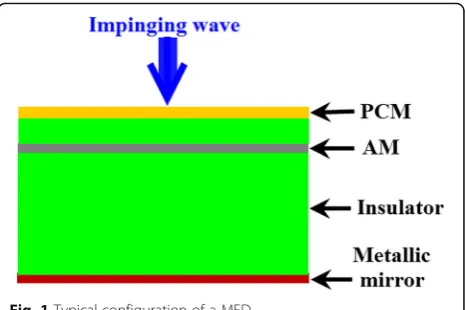
To obtain the capacity of switching between absorption and polarization conversion (PC) modes, the MFD includes two categories of metasurfaces as shown in Fig.1. One type is absorbing metasurface (AM), and the other type is PC metasurface (PCM). A typical configuration of the MFD, as presented in Fig.1, includes PCM structure, AM structure, metallic mirror, and insulators to separate them. It is supposed that, at the absorption mode, the AM dominates the impinging wave and dissipates the incident power, and the PCM is of no avail at this mode. At the PC mode, the AM should be neutralized and the PCM plays a leading role; therefore, the polarization state of the incident wave is converted. To attain the above claims, the key point is the
neutralization of the AM at the PC mode. Therefore, the tunable material should be used to construct the AM, in which the properties of the AM can be tuned. Fortunately, the graphene demonstrates ultra-high electronic mobility and tunable conductivity by adjusting its doping level or electrical grating [26,27]. Therefore, it is advisable to utilize graphene for AM designing. The conductivity of the graphene can be expressed by Kubo formula (1), and it includes intraband and interband contributions.
σs¼σintraðω;μc;Γ;TÞ þσinterðω;μc;Γ;TÞ
σintraðω;μc;Γ;TÞ ¼−j e 2k
BT πℏ2 ω−j
2Γ
ð Þ
μc
kBTþ2 ln e −μc
kBTþ1
σinterðω;μc;Γ;TÞ≅−j e 2
4πℏ ln
2j jμc−ðω−j2ΓÞℏ 2j j þμc ðω−j2ΓÞℏÞ
ð1Þ
where e,ℏ, kB,T, andμcrepresent the charge of an
elec-tron, the reduced Planck’s constant, Boltzmann’s constant, Kelvin’s temperature, and chemical potential, respectively. The Γ is a phenomenological scattering rate, and it is assumed to be independent of energyε. Thus, the complex conductivity σs can be adjusted by tuning the chemical
potential (μc) with biasing voltage. It is found in Eq. (1)
that forμc= 0 eV, the conductivity of the graphene is very
small owing to the low carrier density at this case. Therefore, the graphene operates as a dielectric substrate. Moreover, as the graphene layer is very thin, it has little impact on the illuminated EM waves forμc= 0 eV.
How-ever, the carrier density of the graphene would be raised with increasing chemical potential (μc), and the complex
conductivity (σs) of the graphene is boosted with
in-creasing chemical potential (μc) [26,27]. Therefore, the
graphene supports surface plasmon polaritons (SPPs) for largeμc[26,28–30], and the SPPs confine the incident
waves. To further enhance the SPPs and achieve wave absorption in certain frequencies, periodical structures should be etched in the graphene layer to form a metasur-face, which is called AM. Therefore, by settingμc= 0, the
[image:2.595.306.539.87.242.2]AM can be deemed as a thin dielectric substrate, and it is almost transparent to EM wave. Thereby, the incident EM wave can be concentrated on the PCM layer, and the device operates in the PC mode. For an appropriate largeμc, the enhanced SPPs of the AM confine most of
the incident EM wave, which makes the PCM layer of no avail. Thereby, the incident EM waves are dissipated in the AM layer.
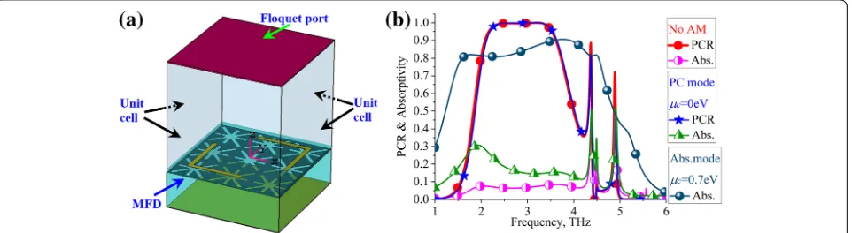
According to the above discussion, a low-profile MFD with gold-based PCM and graphene-based AM is proposed as shown in Fig.2. Figure 2a is a 3D view of a cell. It is found in the figure that one layer of gold-based PCM is printed on the top of the substrate TOPAS polymer [31]. The PCM pattern is a dual L-shaped structure with wide band and good polarization conversion characteristics [18, 19]. As demonstrated in Fig. 2a, a graphene-based AM is inserted in the TOPAS polymer substrate with a distanceh1to the PCM. To endow the graphene-based
AM a dominant role at the absorption mode, the AM should have strong SPPs at a certain chemical potential (μc) to confine most of the incident power and neutralize
the PCM. For this purpose, patterns of cross-slots are etched in a graphene layer, as exhibited in Fig. 2b. It is supposed that the cross-slot patterns bring periodic chan-ging (σ= 0) to the uniformity complex conductivity of the graphene, which leads to charge density rearranging and focusing. Therefore, SPPs are generated and enhanced. The cross-slot structure, as demonstrated in Fig. 2b, is capable of concentrating carrier and fields around the slots, which ensures strong SPPs. The slot lengths of l1
and l2are choosing to ensure the resonances of the AM
fall into operating scope of the PCM; therefore, one cell of the AM has 3 × 3 cross-slot patterns. Note that the PCM and AM are moving and operating independently as their on-off is controlled by the chemical potential (μc);
therefore, the PCM pattern and the AM pattern could be other architectures. The TOPAS polymer is an excellent substrate material for broadband terahertz design, and its refraction index is approximately 1.53 with a very low loss. A gold layer is printed at the bottom of the TOPAS polymer substrate for total reflection. The gold layer is supported by a substrate, which can be Si. The thickness of the gold is 200 nm. Note that the supporting material has no effect on the performances on the MFD as there are no impinging waves penetrating the gold layer. As demonstrated from a 3D view of the array in Fig.2c, the chemical potential can be adjusted through biasing the voltage. The MFD can be fabricated by repeating the growth and transfer process [32,33]. The graphene AM is supposed to haveT= 300 K and momentum relaxation timeτ= 0.1 ps. For PC mode,
μc= 0 eV. The chemical potential for absorption mode is μc= 0.7 eV. The optimized parameters of the MFD are h0= 17 μm, h1= 1.5 μm, l0= 24 μm, W0= 2 μm, l1=
14μm,l2= 19.8μm, andp= 50μm.
Results, Physical Mechanisms, and Discussion Results
The proposed MFD was simulated, and the polarization conversion ratio (PCR) and the absorptivity of the proposed MFD were calculated. As shown in Fig. 3a, the full-wave
[image:3.595.60.538.468.702.2]analyses are conducted in CST Studio Suite with frequency domain solver. Therefore, unit cell boundaries are set at the periphery sides, and a floquet port is set at the top of the calculation region. The PCR and absorptivity of the structure without AM are also plotted in the figure for comparison. Note that the PCR and absorptivity can be cal-culated through the reflection coefficients of the structure since there is no transmission owing to the gold layer [34]. Here, the terms are explicitly defined according to
y-polarized illumination. The electric field of they-polarized incidence wave is defined as Eiy, and the reflected wave
includes a y-polarized electric field (Ery) and x
-polar-ized electric fled (Erx). Then, the reflection coefficients
of co-polarization and cross-polarization are defined as
ryy = Ery/Eiy and rxy = Erx/Eiy, respectively. Therefore,
the PCR and absorptivity can be calculated by Eqs. (2) and (3), respectively. Note that the PCR and absorptivity of x-polarized incidence can be analogously calculated according to Eqs. (2) and (3).
PCR¼r2xy= r2yyþr2xy ð2Þ
Abs:¼1−r2
yy−r2xy ð3Þ
As shown in Fig. 3b, the MFD operates at PC mode withμc= 0 eV, and it works at absorption mode withμc=
0.7 eV. At the PC mode, the structure operates as a polarization converter, and it rotates a linear polarized incident wave to its orthogonal polarization wave. For the PC mode, the PCR is larger than 0.9 in the 2.11–3.63-THz band (53.0% at 2.87 THz), while the absorptivity is small and it ranges from 0.14 to 0.27 in the band. For the struc-ture without AM, it has almost the same PCR band as the PC mode while its absorptivity ranges from 0.06 to 0.09. In the absorption mode, most of the incident wave is
absorbed in the band as demonstrated in the figure. Note that the PCR curve for absorption mode is not presented as it is meaningless. The absorptivity is larger than 80% in the 1.59–4.54-THz band (96.4% at 3.06 THz). Therefore, by adjusting the chemical potential, the proposed structure can switch between PC mode and absorption mode.
Physical Mechanisms
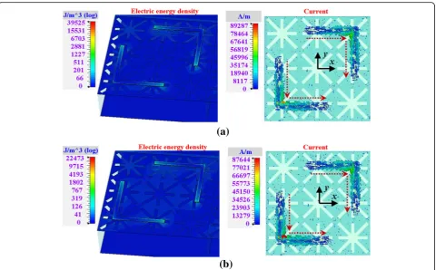
To further reveal the physical mechanisms of the switching characteristics of the two modes, the electric energy densities at the PC mode and the absorption mode of the structure are presented in Figs. 4and 5, respectively. The current distributions of the PC mode are also plotted in Fig.4to state the polarization conversion characteristic. The current distributions of the absorption mode are not illustrated as the currents are attenuated and dissipated at this mode. Note that the field distributions are obtained undery-polarized illuminations.
For the PC mode (μc = 0 eV), two frequencies of
2.56 THz and 3.22 THz are chosen to present their field distributions at Fig.4a and b, respectively. The left parts of the figures are the electric energy densities, and the right parts are the currents. As shown in the figures, the field distributions of 2.56 THz and 3.22 THz are very similar to each other, which imply a wide operating band. From the electric energy densities at the left parts of Fig. 4a, b, the energies are mainly concentrated on the L-shaped structures (PCM). It is indicated that the PCM plays a leading role forμc= 0 eV. From the currents at the
right parts of Fig.4a, b, the currents of both 2.56 THz and 3.22 THz are also concentrated on the PCM, and the cur-rents on the AM are weak. The dotted line arrows indicate the vectors of the currents. The y-polarized illuminations generate x-vector currents on the L-shaped structures, which achieve polarization conversion.
[image:4.595.60.541.540.672.2]For the absorption mode (μc = 0.7 eV), the electric
energy densities of 1.7 THz and 3.3 THz are painted in Fig. 5a and b, respectively. As shown in the figure, the electric energy densities of the two frequencies are mainly distributed on the AM. It is also found that the energies are focused in the cross-slot patterns; therefore, SPP effects are enhanced by the cross-slots on the AM. The strong SPP effects lead to field enhancement on the AM, which endow the AM a dominant role. Thereby, the incident waves are confined and dissipated in the AM. It is also
found that there are still some energies spread on the PCM, which make no perfect absorption, such as 80–90% absorptivity in the band.
Discussion
To further reveal the characteristics of the proposed MFD, parametric studies are discussed in this section. Figure6a and b present the PCR and absorption charac-teristics, respectively, in terms of the chemical potential (μc). As shown in Fig. 6a, a smaller μc means smaller Fig. 4Field distributions of the PC mode (μc= 0 eV).a2.56 THz.b3.22 THz
[image:5.595.59.540.86.384.2] [image:5.595.57.540.571.714.2]conductivity of the AM, and the PCM has a stronger role. Therefore, good PCR is observed withμc= 0 eV, and it is
deteriorated with increasingμc. The absorption
character-istic of the MFD presents almost contrary tendency as shown in Fig.6b. With μc increased from 0 to 1 eV, the
SPPs on the AM are inspired and enhanced. Thus, the incident EM waves are confined in the AM, and the power is absorbed. Theμc= 0.7 eV is chosen for the widest
band-width. It is also noticed in Fig. 6a that the PCR values around 1.85 THz are larger than 80% for 0.7 eV <μc< 1 eV;
however, most of the powers are dissipated for theseμcs as
indicated in Fig.6b. Therefore, the chemical potential (μc)
is a valuable parameter to adjust the PCR and absorption characteristics.
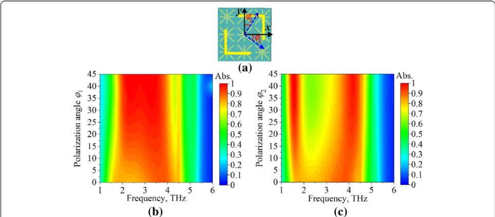
The absorptivity of the absorption mode for different polarization angles (φ1and φ2) is depicted in Fig.7. As
depicted in Fig.7a, theφ1andφ2are the angles of the
in-cident electric fields relative tox- andy-axes, respectively. According to the symmetric structure of the MFD, theφ1
andφ2varied from 0 to 45°. In Fig.7b, as theφ1increased
from 0 to 45°, the absorptivity in the band increased from 0.8 to nearly 1, though the band is narrowed a bit with increasingφ1. As exhibited in Fig.7c, the increasing ofφ2
debases the absorptivity around 2–3 THz, and two absorp-tion bands are obtained around 1.7 THz and 4 THz.
The performances of PC mode and absorption mode in terms of incident angle (θ) are presented in Figs.8and9, respectively. Figure8a and b demonstrate the PCR plots ofs- andp-polarized incident waves, respectively, with the incident angle ranged from 0 to 80°. As shown in the figures, the PCR deteriorated with increasingθ; however, good PCR characteristic is also obtained forθsmaller than
Fig. 6Characteristics of the proposed MFD for different chemical potentials (μc).aPCR.bAbsorption
Fig. 7The absorption characteristics of the absorption mode (μc= 0.7 eV) under normal incidence for different polarization angles (φ).aTheφ1
[image:6.595.60.540.87.241.2] [image:6.595.56.538.490.702.2]40°. The PCR bandwidth is stable to the incident angle (θ). It is also found that the PCR performance ofs-polarized incidence is insensitive to the incident angle (θ) for the frequencies around 2.1 THz.
For the absorption mode, the absorptivity plots ofs- and
p-polarized incident waves are plotted in Fig. 9a and b, respectively, with the incident angle (θ) ranged from 0 to 80°. Generally speaking, the absorptivity of thes-polarized incidence reduced with increasingθ, and the absorptivity is larger than 0.8 forθsmaller than 30°. It is interesting to find that the absorptivity ofp-polarized incident EM wave increased with increasingθ.
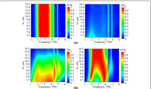
The structure parameter h1 is also studied to further
reveal the multiple functions of the device. As theh1is
adjusted, the position of the AM is changed. Note that other structure parameters are not discussed here for simplicity. Figure10a and b demonstrate the results of the PC mode and absorption mode, respectively. As shown in the left part of Fig.10a, at PC mode, theh1has little impact
on the PCR. In the right part of Fig.10b, the absorptions are also stable forh1ranging from 0.5 to 16.5μm, though
smaller h1 has larger absorption. The results in Fig. 10a
verify the discussions in the “Methods” section, and the AM is operated as thin substrate at PC mode (μc= 0 eV).
For the absorption mode (μc = 0.7 eV), the AM plays a
leading role; therefore, theh1is important at this mode.
As shown in the left part of Fig.10a, the increasing of
h1 decrease the absorptivity. It is because the multiple
reflections and superpositions between the AM and the gold layer are important to inspire the SPPs and enhance the fields on the AM [35]. In the right part of Fig. 10b, good PCR is observed for larger h1. Therefore, in the
designing of the MFD, the parameter h1 can be only
considered in the absorption mode as it has little impact on the PC mode.
Conclusions
In summary, a low-profile and simple structure MFD is proposed by combining gold-based PCM and graphene-based AM. The chemical potential (μc) can be utilized to
activate or neutralize the graphene-based AM, and then, the structure can be transformed from absorber
Fig. 8The PCR characteristics of PC mode (μc= 0 eV) for different incident angles, illuminated byas-polarized andbp-polarized waves
[image:7.595.60.539.87.240.2] [image:7.595.60.539.551.704.2]to polarization converter. For the PC mode, the PCR is larger than 0.9 in the 2.11–3.63-THz band (53.0% at 2.87 THz). For the absorption mode, the absorptivity is larger than 80% in the 1.59–4.54-THz band (96.4% at 3.06 THz). The design may be applied to terahertz imaging, sensing, photodetection, and modulation systems.
Abbreviations
AM:Absorbing metasurface; CP: Circular polarization; EM: Electromagnetic; LP: Linear polarization; MFD: Multi-functional device; PC: Polarization conversion; PCM: Polarization conversion metasurface; PCR: Polarization conversion ratio; SPPs: Surface plasmon polaritons
Acknowledgements
Not applicable.
Funding
National Natural Science Foundation of China under Grant Nos. 61661011 and 61761012.
Availability of Data and Materials
The datasets used and/or analyzed during the current study are available from the corresponding author on reasonable request.
Authors’Contributions
LP developed the concept. LP conducted the simulations. LP, JX, and SML analyzed the results and physical mechanisms. All authors reviewed the manuscript. All authors read and approved the final manuscript.
Competing Interests
The authors declare that they have no competing interests.
Publisher’s Note
Springer Nature remains neutral with regard to jurisdictional claims in published maps and institutional affiliations.
Author details
1Guangxi Key Laboratory of Wireless Wideband Communication and Signal
Processing, Guilin University of Electronic Technology, Guilin 541004, Guangxi, China.2School of Physics, University of Electronic Science and Technology of China, Chengdu 541004, China.3Guangxi University of
Science and Technology, Liuzhou 545006, Guangxi, China.
Received: 19 September 2018 Accepted: 19 November 2018
References
1. Tonouchi M (2007) Cutting-edge terahertz technology. Nat Photonics 1(2): 97–105
2. Jepsen PU, Cooke DG, Koch M (2011) Terahertz spectroscopy and
imaging–modern techniques and applications. Laser Photonics Rev 5(1):124–166 3. Song ZY, Gao Z, Zhang YM, Zhang BL (2014) Terahertz transparency of
optically opaque metallic films. Europhys Lett 106(2):27005
4. Yu P, Besteiro LV, Huang Y, Wu J, Fu L, Tan HH, et al (2018) Broadband metamaterial absorbers. Adv Opt Mater 0(0):1800995.https://doi.org/10. 1002/adom.201800995.
5. Landy NI, Bingham CM, Tyler T, Jokerst N, Smith DR, Padilla WJ (2009) Design, theory, and measurement of a polarization-insensitive absorber for terahertz imaging. Phys Rev B 79(12):125104
6. Liu X, Starr T, Starr AF, Padilla WJ (2010) Infrared spatial and frequency selective metamaterial with near-unity absorbance. Phys Rev Lett 104(20):207403 7. Cui YX, He YR, Jin Y, Ding F, Yang L, Ye YQ, Zhong SM, Lin YY, He SL (2014)
Plasmonic and metamaterial structures as electromagnetic absorbers. Laser Photonics Rev 8(4):495–520
[image:8.595.58.540.86.369.2]8. Alaee R, Albooyeh M, Rockstuhl C (2017) Theory of metasurface based perfect absorbers. J Phys D Appl Phys 50(50):503002
9. Grant J, Ma Y, Saha S, Khalid A, Cumming DR (2011) Polarization insensitive, broadband terahertz metamaterial absorber. Opt Lett 36:3476–3478 10. Pham PH, Zhang W, Quach NV, Li J, Zhou W, Scarmardo D, Brown ER, Burke
PJ (2017) Broadband impedance match to two-dimensional materials in the terahertz domain. Nat Commun 8(1):2233
11. Lv H, Guo Y, Zhao Y, Zhang H, Zhang B, Ji G, Xu ZJ (2016) Achieving tunable electromagnetic absorber via graphene/carbon sphere composites. Carbon 110:130–137
12. Andryieuski A, Lavrinenko AV (2013) Graphene metamaterials based tunable terahertz absorber: effective surface conductivity approach. Opt Express 21: 9144–9155
13. Mou N, Sun S, Dong H, Dong S, He Q, Zhou L, Zhang L (2018)
Hybridization-induced broadband terahertz wave absorption with graphene metasurfaces. Opt Express 26(9):11728–11736
14. Xu Z, Wu D, Liu Y, Liu C, Yu Z, Yu L, Ye H (2018) Design of a tunable ultra-broadband terahertz absorber based on multiple layers of graphene ribbons. Nanoscale Res Lett 13(1):143
15. Amin M, Farhat M, BağcıH (2013) An ultra-broadband multilayered graphene absorber. Opt Express 21(24):29938–29948
16. Li HJ, Ren YZ, Hu JG, Qin M, Wang LL (2018) Wavelength-selective wide-angle light absorption enhancement in monolayers of transition-metal dichalcogenides. J Lightwave Technol 36(16):3236–3241
17. Huo DW, Zhang JW, Wang H, Ren XX, Wang C, Su H, Zhao H (2017) Broadband perfect absorber with monolayer MoS2and hexagonal titanium
nitride nano-disk array. Nanoscale Res Lett 12(1):465
18. Gao X, Singh L, Yang WL, Zheng J, Li H, Zhang W (2017) Bandwidth broadening of a linear polarization converter by near-field metasurface coupling. Sci Rep 7:6817 19. Jing X, Gui X, Zhou P, Hong Z (2018) Physical explanation of Fabry–Pérot
cavity for broadband bilayer metamaterials polarization converter. J Lightwave Technol 36(12):2322–2327
20. Fartookzadeh M (2017) Design of metamirrors for linear to circular polarization conversion with super-octave bandwidth. J Mod Opt 64(18):1854–1861 21. Peng L, Li XF, Jiang X, Li SM (2018) A novel THz half-wave polarization
converter for cross-polarization conversions of both linear and circular polarizations and polarization conversion ratio regulating by graphene. J Lightwave Technol 36(19):4250–4258
22. Ding J, Arigong B, Ren H, Shao J, Zhou M, Lin Y, Zhang H (2015) Mid-infrared tunable dual-frequency cross polarization converters using graphene-based L-shaped nanoslot array. Plasmonics 10(2):351–356 23. Yang C, Luo Y, Guo J, Pu Y, He D, Jiang Y, Liu Z (2016) Wideband tunable
mid-infrared cross polarization converter using rectangle-shape perforated graphene. Opt Express 24(15):16913–16922
24. Cheng H, Chen S, Yu P, Li J, Deng L, Tian J (2013) Mid-infrared tunable optical polarization converter composed of asymmetric graphene nanocrosses. Opt Lett 38(9):1567–1569
25. You JW, Panoiu NC (2018) Polarization control using passive and active crossed graphene gratings. Opt Express 26(2):1882–1894
26. Hanson GW (2008) Dyadic Green’s functions and guided surface waves for a surface conductivity model of graphene. J Appl Phys 103(6):064302 27. Falkovsky LA (2008) Optical properties of graphene. J Phys Conf Ser 129(1):012004 28. Lim GK, Chen ZL, Clark J, Goh RG, Ng WH, Tan HW, Friend RH, Ho PK, Chua
LL (2011) Giant broadband nonlinear optical absorption response in dispersed graphene single sheets. Nat Photonics 5:554–560
29. Bonaccorso F, Sun Z, Hasan T, Ferrari AC (2010) Graphene photonics and optoelectronics. Nat Photonics 4:611–622
30. Tang HH, Huang TJ, Liu JY, Tan Y, Liu PK (2017) Tunable terahertz deep subwavelength imaging based on a graphene monolayer. Sci Rep 7:46283 31. Cunningham PD, Valdes NN, Vallejo FA, Hayden LM, Polishak B, Zhou XH,
Luo JD, Jen AKY, Williams JC, Twieg RJ (2011) Broadband terahertz characterization of the refractive index and absorption of some important polymeric and organic electro-optic materials. J Appl Phys 109(4):043505 32. Yan HG, Li XS, Chandra B, Tulevski G, Wu YQ, Freitag M, Zhu WJ, Avouris P,
Xia FN (2012) Tunable infrared plasmonic devices using graphene/insulator stacks. Nat Nanotechnol 7(5):330
33. Zhang Y, Feng Y, Jiang T, Cao J, Zhao J, Zhu B (2018) Tunable broadband polarization rotator in terahertz frequency based on graphene metamaterial. Carbon 133:170–175
34. Menzel C, Rockstuhl C, Lederer F (2010) Advanced Jones calculus for the classification of periodic metamaterials. Phys Rev A 82(5):053811 35. Chen HT (2012) Interference theory of metamaterial perfect absorbers. Opt