N A N O E X P R E S S
Open Access
Combining scanning probe microscopy and x-ray
spectroscopy
Carole Fauquet
1*, Maël Dehlinger
1, Franck Jandard
1, Sylvain Ferrero
2, Daniel Pailharey
2, Sylvia Larcheri
3,
Roberto Graziola
3, Juris Purans
4, Aniouar Bjeoumikhov
5, Alexei Erko
6, Ivo Zizak
6, Brahim Dahmani
7and
Didier Tonneau
1Abstract
A new versatile tool, combining Shear Force Microscopy and X-Ray Spectroscopy was designed and constructed to obtain simultaneously surface topography and chemical mapping. Using a sharp optical fiber as microscope probe, it is possible to collect locally the visible luminescence of the sample. Results of tests on ZnO and on ZnWO4thin layers are in perfect agreement with that obtained with other conventional techniques. Twin images obtained by simultaneous acquisition in near field of surface topography and of local visible light emitted by the sample under X-Ray irradiation in synchrotron environment are shown. Replacing the optical fibre by an X-ray capillary, it is possible to collect local X-ray fluorescence of the sample. Preliminary results on Co-Ti sample analysis are presented.
Introduction
Non destructive tools providing elemental and chemical analysis at high lateral resolution are needed for life and physical sciences. For example electronics or glass industries need sub-100 nm resolution tools for material processing and control (RRAM, FeRAM, smart materi-als, solar cells) [1]. During the last ten years, numbers of characterization tools were thus developed to obtain with the same apparatus sample imaging and chemical mapping. For example TEM (Transmission Electron Microscopy) is combined with EELS (Electron Energy Loss Spectroscopy) techniques to study oxidation states in transition metal oxides [2]. Near Field Microscopes are powerful tools for surface topography and analysis at nanometric lateral resolution. These equipments allow various in-situ spectroscopies, to probe surface local magnetic properties [3], electronic states [4] or even to identify and localize specific chemical group on very small features [5]. Combination of equipments can give further insights in sample analysis as, e.g. a combination of PEEM with STM [6]. However, those techniques are not simultaneously performed, so that authors had to
mark the surface to recover the PEEM analysis localiza-tion for STM imaging at the same place.
Conventional X-Ray Absorption Spectroscopies are fine analysis techniques providing chemical and struc-tural properties of a material, based on the spectroscopy of the emitted photons or photoelectrons. They require a high brightness X-Ray excitation source, usually a syn-chrotron beam, to irradiate the sample. Emergent high resolution microscopies take advantage of X-ray analysis to perform chemical mapping on samples [7]. For exam-ple, STXM (Scanning Transmission X-Ray Microscope) in transmission mode [7] and XPEEM (X-ray Photoe-mission Electron Microscopy) enable to obtain a sample chemical contrast and electronic structure from indivi-dual nanostructures [8,9].
Coupling X-Ray Spectroscopy and Scanning Probe Microscopy allows collecting with the microscope probe, the sample emission (electron, photons) under X-ray excitation, leading to surface topography and chemi-cal mapping at high resolution at the same place. This concept is now widely investigated in synchrotron envir-onment [10-13].
In this work, we present a versatile Shear Force Microscope head, which can be coupled to an X-ray beam illuminating the sample just at the level of micro-scope probe apex. This micromicro-scope has been fitted to a
* Correspondence: [email protected] 1
Université de la Méditerranée, CNRS-CINaM, Faculté des Sciences de Luminy, case 913, 13288 Marseille cedex 09, France
Full list of author information is available at the end of the article
characteristic of an emitting element present in the material is crossed, the intensity of the visible light dras-tically increases and is followed by oscillations linked to the atomic environment and structure of this element [14]. Chemical mapping was achieved on ZnO and ZnWO4 - ZnO samples.μ-XRF (micro X-Ray
Fluores-cence) analysis was successfully carried out on Co-Ti samples, replacing the optical fibre, microscope probe, by a thin X-ray capillary and using a rotating anode (Cu Ka) as excitation source.
Results Instrumentation
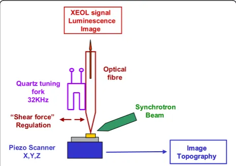
The apparatus consists in an home-made shear-force microscope (see Figure 1) whose probe is a sharp Alu-minium-coated optical fibre (aperture 50 nm) that locally collects the visible light emitted by the sample illuminated by X-Ray radiation (synchrotron environ-ment). The instrument, working in ambient conditions or in liquid environment, allows simultaneous pixel by pixel surface topography measurement and chemical mapping [15]. The analysed sample must fit with Scan-ning Probe Microscopy requirements (solid sample, roughness in the micronscale range). This apparatus is evaluated by characterization of ZnO and ZnWO4
-ZnO thin layers, exhibiting a high luminescence yield. The luminescence spectra are compared to those obtained in far field
focused on the sample by a capillary lens (spot diameter 20μm) provided by IFG GmbH. The XRF technique is particularly suitable for analysis of heavy elements, typi-cally heavier than sodium.
Nano-XAFS-XEOL
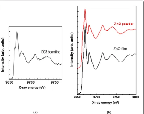
In Figure 2a we present the XAFS-XEOL spectrum obtained with the apparatus at ESRF ID03 line of a ZnO thin layer (~400 nm), prepared by Zn sputtering on a silicon substrate, followed by a 900°C annealing in air. The threshold, localized at 9664 eV, is characteristic of visible light emitted by Zn atoms after X-Ray absorp-tion. This spectrum is compared with that of the same sample (Figure 2b, bottom) and with that of a commer-cial stoichiometric ZnO powder sample for reference (Figure 2b, top, shifted), obtained in conventional XAFS-XEOL spectroscopy, in far field, at the same beamline. Spectra shown in Figure 2b are in very good agreement in terms of both peak positions and relative magnitudes measured with respect to the average signal above threshold. This indicates that the ZnO sputtered layer is stoichiometric. The great concordance between spectra Figure 2a and Figure 2b validates the instrument concept.
A ZnWO4 - ZnO thin layer (~400 nm) was prepared
by co-sputtering Zn and W onto a silicon substrate, fol-lowed by a 900°C annealing in air. In Figure 3 we show twin images corresponding to the simultaneous record of both topography and luminescence cartography of the ZnWO4 - ZnO sample at various incident energies.
In upper Figures 3-a, b, c, d the topography is pre-sented. Grains of 0.5 to more than 1μm are observed, as was confirmed by conventional Atomic Force Micro-scopy. In Figures 3-e, f, g, h we present the correspond-ing luminescence cartography obtained respectively, from the left to the right, before and after the Zn-K edge, as well as before and after the W-L edge. Images 3a to 3 h contain 1024 × 1024 pixels. The remarkable stability of the instrument is noticeable, since it took about 8 h for recording this whole set of images. Image 3 g, obtained at higher X-ray energy than the Zn thresh-old, also highlights Zn rich regions. The contrast is lower than in Figure 3f since the acquisition is per-formed far from the maximum emission. Black zones correspond to non emitting or to grains emitting out of the fibre acceptance angle.
Quartz tuning fork 32KHz
Piezo Scanner X,Y,Z “Shear force”
Regulation
Optical fibre
XEOL signal Luminescence
Image
Image Topography
Image Topography Synchrotron
[image:2.595.57.290.541.704.2]Beam
Post image processing can be carried out on Figure 3e to 3h to define ZnO and ZnWO4 rich areas. First, the
pixel to pixel difference Figure 3f - Figure 3e (resp. Figure 3h - Figure 3g) gives the distribution of Zn (resp. W) luminescent sites. Then, to enhance the contrast, these two images are further converted in black and white scale. By this way we get two intermediate images, which are then used to obtain a chemical mapping of the layer: the ZnO rich emitting areas can be obtained by dif-ference of these intermediate images (Figure 4a), since Zn is present in both materials while W can be found only in ZnWO4grains. Finally, a logic operation‘AND’is
applied between the intermediate images to highlight the distribution of emitting ZnWO4 (Figure 4b) since Zn
must be present in both materials. In fact a white pixel in Figure 4b is obtained only if the same pixel appears simultaneously white on both intermediate images. This image processing leads to a two-level (black and white)
image which increases significantly the contrast. Since Figure 4a shows only few features, one can conclude the emitting centres are almost pure ZnWO4, as confirmed
by XRD and micro-Raman analysis [16]. No obvious cor-relation with the topography is noticeable, since the emit-ting zones are not specifically centered in the grains.
Collecting the XEOL signal in near field significantly increases the lateral resolution of this technique, which is now only limited by the aperture of the optical fibre. In fact, the resolution of the apparatus is limited by the tip curvature for topography (~100 nm) and by the opti-cal aperture for the light collection (~50 nm).
In-labμ-XRF analysis
Replacing the device tuning fork-optical fibre by a fixed X-ray cylindrical capillary the XRF collection concept feasibility is demonstrated on a test sample, composed of bulk Co and Ti juxtaposed sheets. The X-ray beam
(a)
(b)
0,0
0,2
0,4
0,6
0,8
1,0
ID03 beamline
9750
9700
9650
X-ray energy (eV)
Int
e
nsity
(arb.
uni
ts
)
9750
9700
9650
X-ray energy (eV)
Int
e
nsity
(arb.
uni
ts
)
Int
e
nsity
(arb.
uni
ts)
X-ray energy (eV)
Int
e
nsit
y
(a
rb
.
u
ni
ts
)
X-ray energy (eV)
Int
e
nsity
(arb.
uni
ts)
[image:3.595.59.540.87.466.2]X-ray energy (eV)
ZnO film
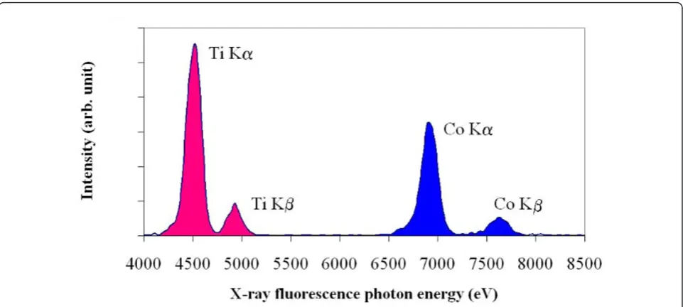
simultaneously illuminates both Co and Ti samples. Fig-ure 5 shows XRF spectra obtained using 10μm diameter cylindrical capillary approached at a distance of 5 mm from the sample surface. We obtain the Ka and Kb characteristic peaks of both Co and Ti, as reported in literature [17]. Since the fluorescence yield of Co is twice that of Ti at excitation energy of 8 keV, the inci-dent spot might be slightly shifted on the titanium sheet regarding the Co-Ti separation.
With commonly marketed XRF equipment, without capillary for detection, the lateral resolution is limited by the diameter of the primary probe, in the range of 10
μm. A resolution increase can be achieved by shrinking down the detector aperture. However, increasing the resolution from 10 to 1μm, would lead to a factor loss of 100 on the signal. To reach the original signal level, the sample-detector distance must be drastically decreased. However the steric hindrance of the EDX
XE
O
L
[image:4.595.58.539.88.295.2]Topography
Figure 3Twin topography-luminescence images. Top: (a-d) topography of a ZnO-ZnWO4sputtered layer (2 × 2μm2). Bottom: corresponding visible light emission cartography under illumination by X-ray beam from left to right below (e) and above (f) the Zn-Kathreshold (9.6 keV) and below (g) and above (h) the W-L3threshold (10.2 keV). On top of the images is indicated the X-ray primary energy.
a
b
[image:4.595.55.542.479.714.2]detector (surface of about 1 cm2) impedes to approach the detector at distances lower than 5 mm. Conse-quently, a solution to avoid primary beam shadowing is to use a low diameter capillary to collect the fluores-cence signal at the vicinity of the surface. Furthermore, using for example a cylindrical capillary to collect the signal enhances significantly the signal level regarding a pinhole of the same diameter at a given sample-detector distance [18]. The gain G is given by:
G =2θcD/d2
Whereθcis the critical angle of the capillary material
(in our case fused silica withθcof about 5 mrad at the
X-ray energy considered in this paper [19]), D is the detector-sample distance and d is the capillary diameter. G is about 3.103 (resp. 3.105) for a 50 mm long and 10
μm (resp. 1 μm) diameter cylindrical capillary approached at 5 mm from the sample surface. More-over, the use of elliptical instead of cylindrical capillary would further increase the signal level by a factor 20 [20,21]. Our experience shows that we can combine X-ray capillary optics for both excitation and detection to substantially increase the resolution of in-lab XRF tech-nique which can be better than 1μm keeping a signifi-cant signal to noise ratio and remaining in satisfactory acquisition times [22].
Conclusion and perspectives
We have constructed a new Shear-Force Microscopy head that is able to simultaneously record the topography and the light emitted by a sample. We have demonstrated
in synchrotron environment the possibility of simulta-neous XEOL mapping and surface topography with a resolution of 50 nm. The instrument is thus able to image the surface and to localize a peculiar object that can be further chemically analyzed by XEOL analysis. Thanks to the recent development of new X-Ray capillary lens, we now equip our home-made Shear Force Micro-scope with a tightly focused laboratory X-ray source for on-table simultaneous Luminescence-Topography mea-surements. The sensitivity of the technique, limited by the signal to noise ratio, will be evaluated in the future.
We have demonstrated the concept feasibility of XRF analysis at micrometer scale. In fact, replacing the opti-cal fibre of our microscope head by a 10 μm diameter cylindrical capillary, we succeeded in local collection of sample XRF under X-ray illumination using an in-lab source. The signal level obtained in this work enables to estimate that the lateral resolution of the technique can still be improved. Consequently sub-1 μm resolution can be reached in lab, whereas, using brighter excitation sources (synchrotron), sub-100 nm resolution is expected, limited today by capillary technology. The final idea is to use an elliptic capillary as shear force probe to simultaneously obtain topography and the XRF mapping of the sample.
Acknowledgements
The authors thank European Community for financial support through FP6-XTIP strep project and FP7-Eureka-Eurostars LUMIX contracts.
Author details
1
[image:5.595.58.539.88.304.2]Université de la Méditerranée, CNRS-CINaM, Faculté des Sciences de Luminy, case 913, 13288 Marseille cedex 09, France2AXESS TECH, 750
microscopy experiments. DP and DT coordinated this study. BD was involved in probe conception and light collection analysis. JP, SL and DT conceived the luminescence experiments and participated in interpretation of data. JP was at the concept origin of coupling scanning probe microscopy and X-Ray spectroscopy. SL, CF and DT performed microscopy data and interpretation. MD, CF, AB and DT conceived theμ-XRF experiments and participated in acquisition and interpretation of data. AB, AE and IZ were involved inμ-XRF data discussion and interpretation. CF, MD and DT drafted the manuscript. All authors read and approved the final manuscript.
Competing interests
Patent concerning the detection of XRF through capillary optics is pending (french patent n°1002392, 2010).
Received: 3 November 2010 Accepted: 7 April 2011 Published: 7 April 2011
References
1. International Technology Roadmap for Semiconductors, 2007 Edition,
Emerging Research Materials.[http://www.itrs.net/Links/2007ITRS/
2007_Chapters/2007_ERM.pdf].
2. Varela M, Oxley MP, Luo W, Tao J, Watanabe M, Lupini AR, Pantelides ST, Pennycook SJ:Atomic-resolution imaging of oxidation states in
manganites.Phys Rev B2009,79: 085117.
3. Rugar D, Mamin HJ, Guethner P, Lambert SE, Stern JE, McFadyen I, Yogi T:
Magnetic force microscopy: General principles and application to
longitudinal recording media.J Appl Phys1990,68: 1169.
4. Pietzsch O, Kubetzka A, Bode M, Wiesendanger R:Spin-Polarized Scanning
Tunneling Spectroscopy of Nanoscale Cobalt Islands on Cu(111).Phys
Rev Lett2004,92: 057202.
5. Duwez AS, Cuenot S, Jerome C, Rapino S, Zerbetto F:Mechanochemistry:
targeted delivery of single molecules.NatureNanotechnology2006,1: 122.
6. Rohmer M, Wiemann C, Munzinger M, Guo L, Aeschlimann M, Bauer M:
Local correlation of photoemission electron spectroscopy and STM at a
defined cluster substrate system.Appl Phys A2006,82: 87.
7. Sakdinawat A, Attwood D:Nanoscale X-Ray imaging.Nat Photon2010,4: 840.
8. Ratto F, Locatelli A, Fontana S, Kharrazi S, Ashtaputre S, Kulkarni SK, Heun S, Rosei F:Chemical Mapping of Individual Semiconductor Nanostructures.
Small2006,3: 401.
9. Fraile Rodriguez A, Kleibert A, Bansmann J, Nolting F:Probing single magnetic nanoparticles by polarization-dependent soft x-ray absorption
spectromicroscopy.J Phys D: Appl Phys2010,43: 474006.
10. Ishii M:Capacitance X-ray absorption fine structure measurement using scanning probe A new method for local structure analysis of surface
defects.Physica B2001, 308-310, 1153.
11. Schmid I, Raabe J, Quitmann C, Vranjkovic S, Hug HJ, Fink RH:NanoXAS, a
novel concept for high resolution microscopy.J of Phys: Conference series
2009,186: 012015.
12. Pailharey D, Mathey Y, Jandard F, Larcheri S, Rocca F, Kuzmin A, Kalendarev R, Purans J, Dalba G, Graziola R, Dhez O:Nanoscale x-ray
absorption spectroscopy using XEOL-SNOM detection mode.Journal of
Physics: Conference Series2007,93: 012038.
13. Eguchi T, Okuda T, Matsushima T, Kataoka A, Harasawa A, Akiyama K, Kinoshita T, Hasegawa Y:Element specific imaging by scanning tunneling
microscopy combined with synchrotron radiation light.Appl Phys Lett
2006,89: 243119.
14. Rogalev A, Goulon J:Chemical Applications of Synchrotron Radiation.In
Advanced Series in Physical Chemistry Part II: X-Rays and Applications. Volume 12.Edited by: Sham TK. World Scientific, Singapore; 2002.
University of California; [http://cxro.lbl.gov/PDF/X-Ray-Data-Booklet.pdf]. 18. Arkadiev V, Bjeoumikhov A: InPractical X-ray Fluorescence Analysis. Volume 3.
Edited by: Beckhoff B, Kanngiesser B, Langhoff N, Wedell R, Wolff H. Springer-Verlag Berlin Heidelberg; 2006: 89-111.
19. Bjeoumikhov A, Bjeoumikhova S: InModern Developments in X-ray and Neutron Optics, Springer series in Optical Sciences. Volume 137.Springer Berlin Heidelberg New York; 2008: 287-306.
20. Bjeoumikhov A, Bjeoumikhova S, Wedell R:Capillary Optics in X-ray
Analytics.Particle and Particle Systems Characterization2006,22: 384.
21. Bjeoumikhov A, Langhoff N, Bjeoumikhova S, Wedell R:Polycapillary Optics
for micro-X-ray Fluorescence Analysis.Review of scientific Instrument2005,
76: 063115.
22. Tonneau D, Purans J, Fauquet C, Jandard F, Erko A, Bjeoumikhov A:
Dispositif de caractérisation topographique et de cartographie chimique
de surfaces.French patent n°10023922010.
doi:10.1186/1556-276X-6-308
Cite this article as:Fauquetet al.:Combining scanning probe microscopy and x-ray spectroscopy.Nanoscale Research Letters2011
6:308.
Submit your manuscript to a
journal and benefi t from:
7 Convenient online submission 7 Rigorous peer review
7 Immediate publication on acceptance 7 Open access: articles freely available online 7 High visibility within the fi eld
7 Retaining the copyright to your article