Technical Description
Technical Description
L-1192 CONTROLLER PROCESSOR
FOR 463-L
SURFACE EQUIPMENT DIVISiON
LIBRASCOPE GROUP
Section l.0 2.0 3.0 4.0 CONTENTS
INTRODUCTION . . . .
SUMMARY OF APPROACH
2.1 Word Format . . . .
2.2 Instruction Efficiency
2.3 Communication Interface
2.4 2.5 2.,6 2. 7 2.8 2.9
Code/Format Flexibility
I/O Stations
ComlTIunic a tion Proc e s sing
I/O Interface . . .
Support Softw.are .
AUTODIN Processing
EQUIPMENT DESCRIPTION AND OPERATION
Co re Merno ry
L-1192 Controller-Processor . .
3.2.1 Arithmetic and Logical Unit 3.2.2 Cornmunication Interface. 3.2.3 Paper Tape, Typewriter, and
Card/Print
r/o . . . .
3.2.4 I/O Interface . . . . 3.2.5 L-1192 Maintenance Panel 3.2.6 L-1192 Inte rval TimerL-1192 INSTR UC TIONS . . . .
4. 1 Fixed Length Charac ter Operations
4.2 Variable Field Operations
4. 3 Fu 11 W 0 r d 0 per at ion s . . . 4.4 Program Control Operations
4.5 Internal Condition Operations
4.6 Communication Interface Operations
4.7 Input/Output Operations
Page
1 - 1
2 -1 2 -1 2 -1 2 -1 2 -1 2-2 2-2 2-2 2-2 2 -3 3 -1 3 -1 3 -1 3 -1 3-7 3-9 3 -1 0 3-10 3 -14
4 -1
4 -1
4-8
4 -12
4 -14
4-15
4 -16
4 -18
Sec tion
5.0
6.0
7.0
CONTENTS - Continued
PERIPHERAL EQUIPMENT
5.1 Line Unit Console
5.2 Model 2250 Systerr1atlcs Card/Printer Input/ Output Stations . . . .
5.2.1 Operating Modes 5.2.2 Operating Speed S. 2. 3 Station Devices
5.3 Magnetic Tape Console
5. 3. 1 Tape Transport On - Line Read 5.3.2 Tape Transport On-Line Write 5.3.3 Tape Transport Off-Line Operation
(optional) . . . .
S.4 Card Reader /Punch Console
5.4.1 Card Reader 5.4.2 Card Punch
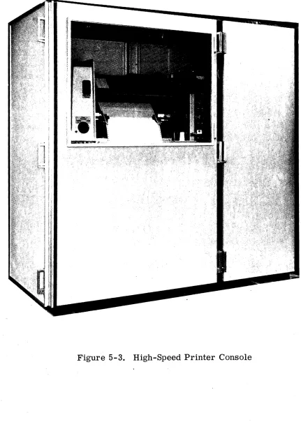
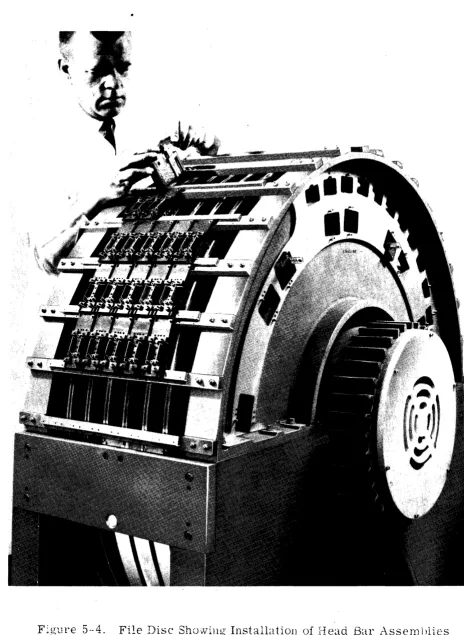
5.5 High-Speed Printer Console S.6 Master Disc File Console . . .
SUPPOR T SOFTW ARE AND PROGRk.Y1MING DESCRIPTION . . . .
6. 1 LAP-l192 Assembler 6.1.1 Purpose . . . . 6. 1.2 Equiprnent Required
6. 1. 3 Input l\1edia . . 6.1.4 Output Media 6.1.S Features . . .
6. 1.6 Input Forrnat . . . 6. 1.7 Pseudo-Operation
6.2 System Loader . . . .
6.3 Core and Disc Dump
6.4 Acceptance Tests
AUTODI0J PROCESSING
7. 1 Input Proce s sing
7. 1. 1 Characte r Frarne . . 7.1.2 System States . . . .
Page 5-1 S-l 5-2 5-2 5-3 5-3 5-5 5-6 5-8 5-8 5-9 5-9 5-11
5 -1 1
5-13
6-1
6 -1
6-1
6
-1Section Figure 1 -1 3 -1 3 -2 3 -3 3-4 4-1 5-1 5-2 5-3 5-4 7-1 7-2 7-3 7-4
CONTENTS - Continued
7.1.3 Start of Block Processing . . 7.1.4 Data Characters . . . 7.1.5 End of Block Operations
7.2 Output Processing . . . .
7.3
7.2.1 Character Franle . . . . • 7.2.2 Start of Block Processing •. 7.2.3 Data Characters . . . 7.2.4 End of Block Operations . .
Channel Coordination . . . .
7.3. 1 Input Channel Coordination. 7.3.2 Proces.sing of RM and DM
7.3.3 Establishrnent of Acknowledge Sync on Startup . . . .
ILLUSTRATIONS
L-1192 Configuration for 463-L . . . .
L-1192 Buffer Processor Console - Front View.
L-1192 Buffe r Proce s sor Console - Rear View
L-1192 Buffer Processor, Block Diagralll . .
L-1192 Maintenance Panel
Register Selection . . .
Magnetic Tape Console Control Panel
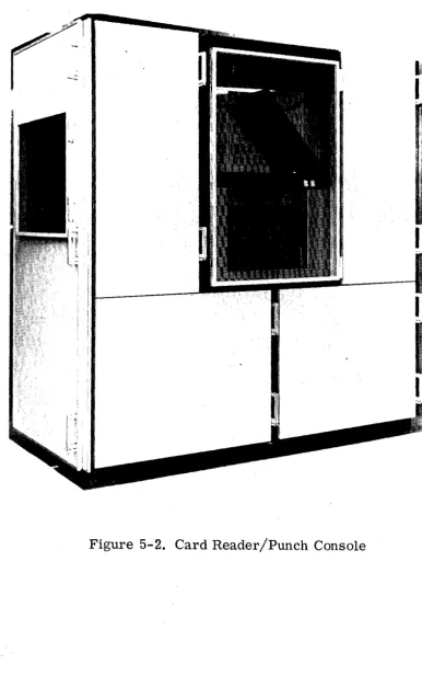
Card Reader/Punch Console.
High-Speed Printer Console.
File Disc Showing Installation of Hear Bar Assemblies . . . .
AUTODIN Program - Overall Flowchart.
Input Character Processing.
Output Character Processing
Channel Coordination Processing
Page 7-4 7-5 7-5 7-6 7-6 7 -0 7-8 7-8 7-8
7-10
7 -11
7-14 Page 1 -2 3 -2 3 -3 3 -5
3 -1 1
Section 1
INTRODUCTION
This docurnent presents a technical description of an intransite cargo
con-trol systern for 463-L. The equipment will be utilized to concon-trol and
rnonitor the movernent of air cargo by storing and providing shipping
infor-mation for ternlinal operations. The Librascope design approach is
based prirnarily on experience gained from their L-3055 data processing
system. This equipment was developed and fabricated under contract to
the U. S. Air Force, and has been installed in the Pentagon as the
AN/FYQ-ll data processing element of Command and Control System
473 -L.
The following equiprnent is offered as a L-ll92 Controller-Processor
system for 463 -L. A machine configuration is presented in Figure 1-1.
• 1 L-1192 Controller-Processor Console
• 1 Paper Tape Reader, Punch, and Electric Typewriter
• 2 Core Memory Module s, total 8192 words
• 1 Magnetic Tape Console, providing 2 transports
• 7 Card/Print Input-Output Stations
• 1 Forty Million Character Disc File
The L-1192 system provides a binary computer, with both an AUTODI?\
communication interface and general purpose processing capability. It
may be expanded to address up to 65,536 32-bit plus parity bit v,:ords of
core memory. Each word may contain eithe r one instruction, four 8 - bit
characters, or a 32-bit binary operand. The L-l192 will operate with a
great num be r and variety of pe ripheral device s, including magnetic tape,
card reader/punch, disc file, high speed line printer and input-output
card/print stations. It will also interface with the alphanumeric L-3155
Central Processor, which provides eight 7-bit characters per COlTIputer
word.
I/O STATION I
CARD CARD
READ PUNCH PRINT
f
I/O STATION 2
I
I
~C-A-R-D~--CA-R-D~----~L
___~J
PRINTI
:1 READ PUNCHI
I/O STATION 3!
PAPER PAPER ELEC. MAG
CARD CARD PRINT
I
READ PUNCH TYPE TAPEREAD PUNCH
I/O STATION 4 L-1192
I/O CHANNEL
CARD CARD PRINT CONTROLLER-PROCESSOR
READ PUNCH
I/O STATION 5
CORE MEMORY
CARD CARD PRINT DISC
READ PUNCH
8192 WORDS
I/O STATION 6
,
CARD CARD PRINT READ PUNCH
I/O STATION 7
[image:7.612.49.540.74.681.2]CARD CARD PRINT
-READ PU'NCHFigure
1-1. L-1192 Configuration for 463-L
\
,
,
.
MAG TAPE
FILE
A prograrnming manual for the L- 31 55, a s the central cornpute r in <in
L-3055 data processing system, is included under separate cover. The
L-3155 will operate with the same peripheral devices as described for
the L-1192 systern. An L-3155 Central Processor, with 8000 words of
core nlemory and the same pe riphe ral equipment configuration, is also
proposed as an alternate to the L-1192 system.
Section 2
SUMMAR Y OF APPROACH
The L-1192 Controller Processor is a general purpose computer system,
with special emphasis on the efficient processing of input-output and
communication data.
2. 1 WORD FORMA T
The L-1192 provides 2 microsecond cycle cone memory in modules of
4096 words, with a maximum capacity of 65,536 words. The 33 -bits per
word includes 32 data bits, providing four 8-bit characters, plus one
parity bit. This word length permits an instruction format well suited
to characte r proces sing and addre ssing.
2 .. 2 INSTRUCTION EFFICIENCY
The L-1192 offers three categories of processor instructions: single
char-acted operations, variable -length field operations, and full-word operations.
The single character instructions utilize a group of eight arithn1etic
regis-ters, which eliminates the bottleneck normally encountered in processing
lTIultiple input-output data.
2.3 COMMUNICATION INTERFACE
The L-1192 Console can communicate with up to four duplex
cornn1unica-tion channels, by the addicornn1unica-tion of the proper interface modules. This
capa-bility can be expanded to 64 duplex channels by means of an optional Line
Unit Console. Any mix of asynchronous and synchronous line s is
per-missible. Asynchronous lines operat~ up to 150 bits/sec, and synchronous lines at up to 4800 bits/sec.
2.4 CODE/FORMAT FLEXIBILITY
The L-1192 has been designed to efficiently process AUTODIK
conJlTIunica-tion requirements. Care has been exercised to permit flexibility of
operation through program modification. Desired character codes,
for-mats, and channel coordination procedures are under control of the stored
program.
2.5 I/O STATIONS
The Standard Communication Interface will also cOlnrnunicate with up to
eight input/output stations, which may be located at remote positions.
One station is utilized by the 300 char/sec paper tape reader, 60 char/sec
paper tape punch, and 15 char/sec electric typewriter at the Ope rator /
Maintenance PaneL The other seven stations each provide a 20 char / sec
card read, 20 char/sec card punch, and a 40 char/sec printer position.
The number of I/O stations may be expanded in groups of 8 to a total of 32.
2.6 COMMUNICATION PROCESSING
Input characters and output requests for the cOlnmunication channels and
the I/O Stations automatically enter cyclic. Channel Activity Tables
re-served in core memory. These entries do not interrupt the system, and
are accessible to the computer program for further processing.
2.7 I/O INTERFACE
One I/O Inte rface is provided with the L-119l Controller Proce s sor, and
up to sixteen interfaces may be utilized. Each interface may comn'1unicate
with up to sixteen standard Librascope peripheral devices. These include
magnetic tape, card reader/punch, high- speed line printer J and disc file
equipment.
2. 8 SUPPOR T SOFTWARE
The support software offered with the L-119l system includes an Assembler,
a System Loader, Core and Disc Dump, and Acceptance Test.
2.9 AUTODIN PROCESSING
Librascope has had extensive experience in processing communication
data, and will be available to assist in n1eeting AUTODIN requirements.
An operational approach developed for the L-l192 sy stem is pre sented
in this propo sal.
Section 3
EQUIPMENT DESC RIPTION AND OPERATION
This section discusses the design and operation of each iteTn of equipment
available with the L-1192 Controller-Processor system.
3.1 CORE MEMORY
Core menlory for the,L-1192 Controller-Processor systenl is provided in
modules of 4096 words. The L-1192 may address up to a maximum of
six-teen rnodules, for a total of 65,536 words of memory. A word contains 32
data bits plus an additional bit to rnaintain odd parity. Each data word
pro-vides four 8-bit characters, which may be individually addressed by L-1192
instructions. Transfers to and from core memory are in word parallel,
and these are parity checked. The core memory modules offer a
read-write cycle time of 2. 0 microseconds. The transfers between core
n'lem-ory and the central processor arithnletic/logical unit, the cOlnrnunication
interface, and the input-output interface all overlap on a cycle stealing
basis.
3.2 L-1192 CONTROLLER-PROCESSOR
The L-1192 Controller-Processor consists of an Arithmetic and Logical
Unit, a Communication Interface, Paper Tape Reader/Punch and Electric
Typewriter, an I/O Interface, and the Maintenance Panel, and an Interval
Timer. The L-1192 Console is presented in Figures 3-1 and 3-2.
3.2.1 Arithmetic and Logical Unit
The L-1192 ALU includes the instruction register and instruction decode
logic, individually addressable character-length data registers, a Field
Operand Address Register, and two full-word arithmetic registers.
The simple yet flexible organization of the L-1192 is apparent froni the
block diagram of the processor organization, presented in Figure 3 -3 any
operations which involve two operands can'be obtained in any conlbination
from the data or word regis'ters and memory by general bus logic. The
0J
,
tv
CONTROL PAf·JEL
Figure 3-1.
CIRCUIT
AND nEL~nEAKER Y PANEL
INPUT-C'U1A . r'UT r' \,.~. NO H~r;'Ul-. f' .... '0" Tt '1 n t '" .•... T<' .)
•• '- 0\ f. ': ~·t\
L-1192
Buffc.I'Pro
ccssor ~,.
C
ollsule
- Front
\T' [image:13.802.51.737.48.549.2]C/~RD RACr\ ~-.c-_____
CARD R/\CK
m---!-~VOLT".GE
REGULATORIrl---l~FUJ
CASO:-
~---
11--.
PO~IEfl
SUPPLIESA-_~~_
llL
FAN CAGEI
r---______
--!!~.
POWER SUPPLIES'~l
-
Hcar Viewff
r
P rocc~sorConso
c
[image:14.793.42.742.62.541.2]function of address IT1odification is also perforn1ed by this technique.
Com-n'lunication with the core mernory is by an address and word bus which is
time shared with the Comrnunications Interface and with the I/O Interface.
3.2. 1.1 Data Forn'lat. Each L-ll92 word consists of 32 data bits plus
one parity bit. Four 8 -bit data characters are contained in a word, and
these characters may be individually selected by the L-l192 instruction.
8 8 8 8
Character Character Character Character
P
4 3 2 1
3.2. 1.2 Instruction Format. Instructions are one word in length, and
permit register selection in addition to memory word addres sing. Special
features of the instruction set include direct character selection, word
and character indexing, indirect addressing for both memory and registers,
and the inc lusion of specialized instructions.
3.2.1.3 :tv1emory Addressing. The address field of an instruction provides
for direct reference to anyone of 65,536 words of core memory. In
addi-tion, 2 bits appended to the low order end of the address field perrnit the
selection of an individual character within the word. This feature provides
full-character addressing.
~
3.2.1.4 Processor Instructions. The L-1192 offers three categories of
processor instructions. Fixed length character instructions primarily
provide single-character transfer, arithn'letic, and logical operations.
These facilitate the processing of data from rnultiple comn1unication lines
and direct-coupled paper tape, punched card, and typewriter/printer
de-vices. A set of variable field (up to 16 character) instructions provide
added formatting and editing capability for both communication and
input-output: devices. Word-length operations are also provided to meet higher
speed processing requirements.
lNSTR. REGiSTER
J
P COUNTER
I
~
y
--=-~
______
,
.... ____
-..:a _ _ _ _ _ _ _ _ . . - -_ _ _ _ _ _ _I
I
I !
I
~'I'
II "/ '\ ',1 !\ \:";~,
~ tl ,CHt.RACTER CHAAt.CTER
a
DATA CHARt.CTER •~
LA
B REGISTERS I HII
J,~.,
_J ... , __
J~~~
__
OPE_RAND I BUSr\\
I
,
I
O?ERh:-;O \ - • \ \ \I
2 eLiS ,1 "J <:,. ,< "I
i
~
~----~---C-4~C'3C2C~
I
HI
L
\:'
LOGICAL\~,
C~~fE~~ER
.. /~)- AtW RESULT BUS
~;-
-~CONTROL
-~~kT~~~~~
*
~
~ I
~
~
N i!
~
I
I'-o---L:(
CONTROL)I
FIELD"'. OPERA~D
--"'1
ADDRESSREGISTER
WORD REG.
R
~: 1
~
WO~;) R:::G.
I
Q I
" - -_ _ - - - - J
I
"
, I
1':"-\-! i
VAR!A3~E F!ELD
OPERATIONS
O?TION
\-,/
~-~
.. : r:-c-".--L-E-~:-G-T;--;
-C-i":.)-::'-'\;"-· r-; c-' ;\-, s ... ;i
CPI"; Or,,; j !
Figure 3-3. L-1192 Buffer Processor, Block
Diagran1
[image:16.618.82.560.39.698.2]3.2.1.5 Specialized Instructions. Several of the L-1192 instructions have
been specialized in order to enhance speed-cost effectiveness in
conuYluni-cation and input-output processing. The i:1C~l;s:()n of these instructions
combine the advantages of wired logic with t : l l ' j"Lexibility of stored prograrn
con t r 0 1. An In it i ate C h a r act e r C y c 1 e ins t rue t i (j n , for e x amp 1 e , wi 11 e ff i
-ciently locate and access the next input character or output request to be
processed. These were automatically stored in core rnel110ry Channel
Activity Tables (CAT) by the L-1192 hardware.
3.2.1.6 Character D~ta Registers. The L-1192 15 provided with a set
of 8 character-length static registers, which are basic to its list of
power-ful character processing instructions and capabilities. Any of the 8
reg-isters may be utilized in arithn1etic, data, or logical operations. Most
operations involve a single register and a location in core H1ernory.
Op-erations may also be specified which involve only a pair of registers, or
a register and an operand or mask contained in the instruction word itself.
These features serve to reduce the amount of time normally consumed by
computers in the access and storing of operands in core memory. The
unusually high character processing efficiency of the L-1192 is attained by
rnaking up to 8 separate data itelTI s immediately available to the arithmetic
unit.
The data registers may also function as index registers. \\Then used as
index registers, four of the 8-bit data registers operate independently.
Each can provide a total modification of 256 character or 64-word
ad-dresses. The remaining four are paired to provide two 16-bit index
reg-isters, each with an addressing capacity of 65,536 characters. Indirect
addressing is also a feature of the L-1192, and may extend over any
num-ber of levels. Indexing is effective at each indirect level.
3.2. 1.7 Additional Registers. The variable field instructions provide
rnemory to memory operations. One operand address and field length is
normally specified by the instruction word. The second operand address
and field lengthmustfirst be loaded into a Field Operand Address
Regis-ter (FOAR). The ful
f
-word instructions utilize two independent wordarithrnetic registers (R and Q). The variable field instructions and the full-word instructions also utilize the character data registers as index
registers. They are available as arithmetic registers only to the fixed
length character instructions.
3.2.1.8 Error Checks. To insure rnessage protection, the L-1192
em-ploys several internal error checks. These include an automatic test of
word parity when a word is transfe rred fronl C orc mernory, and pa ri ty
c he c k son t ran s fer 0 per a t ion s be tw c en the L -1 1 92 and the I/O per i
r
her a 1devices. Prograln testing is normally utilized to parity check
charCic-ters received frorn the communication lines.
3.2.1.9 Interrupts. To perlnit efficient servicing of the Input-Output and
Con1n1unication Interfaces, a nun1ber of interrupts have been provided.
The conditions which can cause an interrupt include: Interval Tirner
elapsed, I/O operation ended, service requests from the peripheral
de-vices, and internal or input-output parity error.
When an interrupt occurs, the content of the P counter and a bit
indicat-Ing the cause of the interrupt are stored in core memory location
¢,
and the next instruction is taken from location 1. All other interrupts are then. prevented fronl occurring. They may be enabled by use of the ESI or PSIinstructions.
3.2.2 COD"nnunication Interface
The Communication Interface is contained in the L-1192
Controller-Processor Console. It controls the transfers of data between core mernory
and on-line communic ation channels or device s.
The basic systen1 can accornmodate four input and four output c on1nlunic
a-tion channe,ls, by the addia-tion of opa-tional Line Interface :-'lodules. ).,:odules
may be specified fo r async hronous or for sync 11 ronou s transll.li s s ion at
rates up to 4800 baud. The C0111111unication interface ea?ability car', be
expanded by the addition of an optional Line Unit Console, which can
Lie-commodate up to 64 input and 64 output COl1lll1unic ation inte r face l11.ociule s
and c hanne ls.
3.2.2.1 Core Buffering. Character buffering is provided by the interface
rnodules, while rnessage blocks are accunlulated in core melnory. This
approach results in significant saving in systerll cost, and pernjits the
progranj to operate asynchronously with line rates.
The core buffering operation is performed in a unique and efficient
Inan-nero Two cyclic table areas, narned Channel Activity Tables, are
re-served in core mernory. These are automatically loaded by the
Cornnjuni-cation Interface with the input characters or with requests for output
characters, each with a line identity number. Channel Activity Table 1
(CAT 1) is reserved for character requests luade by high speed output
lines. Channel Activity Table 2 (CAT 2) is used to buffer all other lower
priority output requests and all input traffic. CAT 1 may contain 128
entries or words in nJenJory, while CAT 2 has a capacity of 256 entries.
3.2.2.2 COlnulunication Line Servicing. The COlTInjunication Interface
nJakes use of two cyclic load address registers designated Ll and L2, for
CAT 1 and CAT 2 control respectively. Each tilne an entry is to be stored
in either table, the appropriate load counter provides the required core
loading address and is then stepped. CAT 1 and CAT 2 are unloaded and
processed by means of two other cyclic address counters, nanied VI and
U2 .. A nJore detailed discussion of the procedure for unloading of CAT 1
and CAT 2 is contained in the discussion of the Initiate Character Cycle
instrU"ction, found in Section 4.6.
The output characters transnJitted in response to output requests are
auto-nJatically obtained fronl. another table, nanJed the Line Character Buffer
Table. The LCBT contains one assigned character address in core
l1l.er11-ory for each output line inJplenJented. These output locations are loci.ded
by the progranJ with the next output character for the corresponding line
nuniber. \Vhen an output interface nJodule has cOnJplctely transrnitted an
output character it initiates an interface available signal, which will be
detected by and halt the scanners in both the Line Unit Console and in
Conl.-rnunication Interface. The two scanner positions will generate the proper
character nJenjory address in the LCBT, and the character at this position
will transfer to the waiting output linc interf;IC(~ 11lodule. The
Curilrnuni-cation Interface will then load an output request, including the linc
identi-fication nurnber, into CAT 2 {for high speed lines} or into CAT 1 (for slow
speed lines). The Ll or L2 load point is stepped, and the scanners are
r e lea sed to con tin u e sea r chi n g for 0 the r in put 0 r 0 u tp u t t r a ff i c . In put
traffic is handled in a sOlTIewhat sirnilar manner by the Cornmunication
Interface. When a complete character has been accuHlulated by an input
line interface lTIodule, it sets a signal causing the scanners to stop.
1Vlem-ory access is obtained, and the character plus the associated line number
is automatically transferred to the next available word location in CAT 2.
The L2 loa~ point is stepped, and the scanners are then released to
con-tinue looking for traffic ~ The input character will be proc es sed by the
L-1192 program, whos.' instructions can efficiently access the next input
character or output request from the two Channel Activity Tables.
3.2.2.3 Channel Activity Table Forn1ats. The following inforn1ation
pro-vides the word formats loaded into the Channel Activity Tables (CAT) for
the input character s and the output reque sts.
8 8 8
I
I
Input
Entry Not Used
I I
Line/Device
0 Input Ch?.r.
Address Output Request 3.2.3 I I
I Line/Device
Not Used I 1
I Address
I
Paper Tape, Typewriter, and Card/Print I/O
Al\vay s Zero
The basic Comnlunication Interface also cornmunicates with up to eight
direct-connected input-output stations, which lTIay be located at rernote
sites. The number of such stations accessible to the comrnunication
inter-face may be optionally increased in groups of eight up to a total capacity
of 32 such stations. the paper tape reader, punch, and IBlvl keyboard/
typewriter at the COlTIputer console provlde one station position. A
Kleinschrnidt keyboard/printer, and a card reader/punch are located at
each of the other seven station position. A switch at each station
per-mi ts: keyboard input, card reade r input, punch output, print output, and
3-9
print/punch output operation. Transfers to or frorn these devices arc
character-serial, with up to 8 bits/char.
3.2.4
1/
a
Inte r fac eThe I/O Interface provides for data transfers to and from the sta.ndard line
of Librascope nlagnetic tape, card reader/punch, line printer, and disc
file equipment. These peripheral devices are presently utilized in the
Librascope AN/FYQ-ll Data Proc'essor Set for the Headquarters U. S.
Air Force 437 -L Command and Control System. All data transfer to and
froID these devices occur on an asynchronous basis, with the I/O interface
obtaining rnemory access priority as needed. The I/O interface will
in-dependently execute interface block transfers, and overlap central
proc-essor operations.
3.2.4.1 Desc ript.ion. The I/O interface contains a Device Con1nland
Register, a Block Control Register, an Interface Data Register, a
Corn-Inand Address Register, and associated control and bus logic. Once the
interface has been placed in operation, it will access a device Comrnand
Word and a Block Control Wor.d from core nlemory. The Cornnl.and \\Tord
specifies the device and cO'mlnand operation. The Block Control word
designates the Inemory starting address and the required nUIDber of
characters. Data is shifted into or out of the Interface Data Register In
a character-serial fashion on a device demand basis. As data is
trans-ferred, the Block Control Register counts characters and nlernory
loca-tions. When the Block Control word is satisfied, the operation is
ter-nlinated and the main processor program is interrupted.
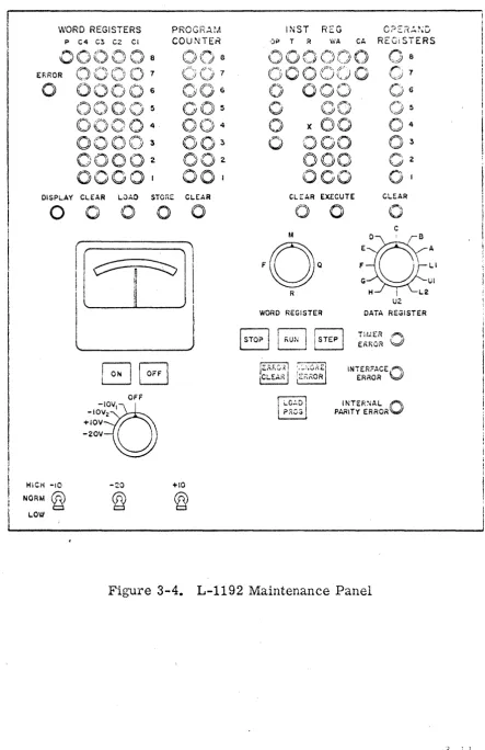
3.2.5 L-1192 Maintenance Panel
The maintenance panel, presented in Figure 3 -4, contains the necessary
controls and indicators for performing preventive or corrective
nlainte-nance on the L-1192 Controller-Processor and its interfaces. By rneans
of these controls and indicators, the various internal registers are
dis-played and their contents may be altered. In Clddition, L-ll92 error
WORD REGISTERS
P C4 C3 C2 CI
PROGR~M
COUNTER
OOe
(:;-~\. 1';';;;. 7 ~)V
fT";;,
0"\\
6U ~A
-r-:
0"'"vO
500
400
3.F':l r)} 2
~v
001
DISPLAY CLEAR LOAO STOlil: CLEAR
o
HICK -10
NORM ~
LOW
o
o o
OFF
-IOV2 I .
+IOV
-20V-oOV
-~oo
+10CLEAR EXECUTE
o
0
M
R WORD REGISTER
REGi STERS
0
8,r'··
~) 7 (0.;.) G
~ CLEAR
o
C:~:,
G?M-,UI
H I 1..2 U2 OATA REGISTER
INTER~~AL
O.
PARITY ERRORFigure 3-4. L-1192 Maintenance Panel
[image:22.615.91.535.74.759.2]indicators rnay be reset fron1 this panel. The output voltages of the
vari-ous power supplies may be n1casured, and their outputs biased to assist
in detecting n1achine malfunctions. The following paragraphs dcsc rihe in
detail the functions of the various controls and indic9-tors on the
m.:linte-nanc e pane 1.
3.2.5.1 Word Register Display and Switches. An array of 33 pushbutton
indicator/switches displays the content of the specified word register.
Selection of the Memory Access Register (M), the Field Operand Access
Registers (F), or the word arthmetic Rand Q Registers is by n1eans of a "Word Register" select switch. The display is arranged into 4
char-acters of eight bits each and the parity bit. An associated error indicator
is illun1.inated when the n1.en1.ory register is selected and contains a parity
fault c ondi tion (even nurnbe r of bi ts) ... Direc t manual n1emory entry is
performed using the Clear and Load pushbutton switches. The Clear
pushbutton clears the selected register to binary zeros, except for the
parity bit which is a binary one to maintain required odd parity. The
desired word is then set by pushing appropriate register pushbuttons.
Pushi?g the parity pushbutton will set the correct parity bit and reset the
error indicator.
Pressing the STORE pushbutton stores the contents of the selected
regis-ter into the address specified by the W portion of the Instruction Regisregis-ter.
W is then incremented by one. The content of the memory location
speci-fied by W may be displayed by pressing the DISPLAY button, which also
causes W to increment by one.
3.2.5.2 Program Counter Display and Controls. An array of pushbutton
indicators displays the content of the program counter. The "PROGRAlvl
COU~TER" display can be set to zero by the associated "CLEAR"
push-button and new content set in manually.
3.2.5.3 Instruction Registe r Display and Controls. An array of
push-button indicators displays by fields the content of the instruction register.
The "INST REG" display can be cleared by the associated "CLEAR"
pushbutton and new content set in n1.anually. The currently contained
in-struction can be executed in stop n1.ode by pushing the "EXECUTE" 1)utton,
pern1.itting instruction processing without counting up the progran1 counter
or leaving the stop n1.ode.
3.2.5.4 Operand Registers Display and Controls. The "OPERAT\D
REGISTERS" display pushbutton indicators n1.ay be used to observe the
content of any of the 8 Data Registers, or the content of the two Load and
Unload Counters assqciated with the con1n1unication interface. Selection
of register or counter to be displayed is controlled by a rotary II DA T A
REGISTER" switch below the "OPERAND REGISTERS" indicators. The
register currently displayed n1.ay have its content cleared to zero by means
of the "CLEAR" pushbutton and a new content n1.anually entered.
3.2.5.5 Error Indicators. The three error indicators in the lower
right-hand section of the panel display detail errors detected by the L-1192
hard-ware. The "INTERNAL PARITY ERROR" indicator will light whenever the
L-ll92 hardware detects a word parity error on transfers to or from
core memory.
The "INTERFACE ERROR" indicator will light whenever the L-1192
inter-face logic detects a character parity error on input-output data transfers.
The "TIMER ERROR" indicator will light whenever the INTERVAL TI;\/lER
counts down to zero.
3.2.5.6 Operating Controls. The ON and OFF buttons control the
a.ppli-cation of power. Pressing the RUN button will cause the L-ll92 to locate and execute instructions at normal operating speed until either a HALT
comrnand is decoded, the STOP button is pre:::: St:d, or an internal error IS
detected. The STEP button will cause a single instruction to be executed
each tin1.e the button is pressed. Operation of the ERROR CLEAR will
reset all error toggles.
3.2.5.7 Error Controls. The "ERROR CLEAR'I
pU!:5hbutton resets all
error indicators.
The "IGNORE ERROR II pushbutton disahle!:5 the halt on ins truc tion pari ty
error and may be used while operating diagnostic or rnainfenance progra.ms.
3.2.5.8 Power Supply Monitor and Controls. By IT1eanS of the associated
selector switch, output voltages of the various power supplies in the L-1192
may be displayed on the n1eter on the lower left-hand portion of the
n1ain-tenance panel. Toggle switches are provided to control increase or
de-crease of power supply voltages in the diagnosis of machine nl.alfunctions.
3.2.6 L-1192 Interval Tin1er
The L-1192 Interval Tin1er is an electronic counter operated by the n1aster
logic clock. It is cOn1posed of 32 bits (one word). It counts down by one
during each clock period. It can be pre-set under prograrn control via the
I/O interface, and its current value can similarly be stored in core.
The nl.axin1un1 pre -set value is equivalent to approximately one hour.
Re-solution is approxinlately ten times greater than the instruction execution
rate.
Section 4
L-1192 INSTRUCTIONS
The detailed de scriptions of L-1192 instructions have been grouped under
the following gene ral categorie s:
1. Fixed Length Character Operations
2. Variable Field Operations
3. Full Word Ope rations
,
4. Prograf!l Control Operations
5. Inte rnal Condition Ope rations
6.
Communication Interface Operations7 . Input/Output Ope rations
The timing provided with each instruction include s instruction and operand
access, and is give'n in memory cycles (each 2 microse'conas). If
in-direct addre ssing is employed, one cycle must be added for each inin-direct
level. Indexing doe s not increase the instruction time. ,
4.1 FIXED LENGTH CHARACTER OPERA TIONS
The se instructions provide for moving,' comparing, modifying or
per-forming arithmetic operations on single-character or fixed-length
multi-ple character fields. These instructions are primarily used for
perform-ing characte r buffe rperform-ing functions. Mo st of them pe rm it the selection of
one of eight single character data registers in which the operation is to
be performed. Those operations which address core memory also may
specify indirect addressing, as well as indexing by one of six groups of
character registers. If indirect addressing is designated, each indirect
level may be independently indexed. Indexing doe s not normally increase
the execution time, but each indirect level add~ one memory cycle.
The table shown below shows the general format for L-1192 fixed length
character instructions. Where an individual instruction deviates from
this format, the change is described in detail.
6
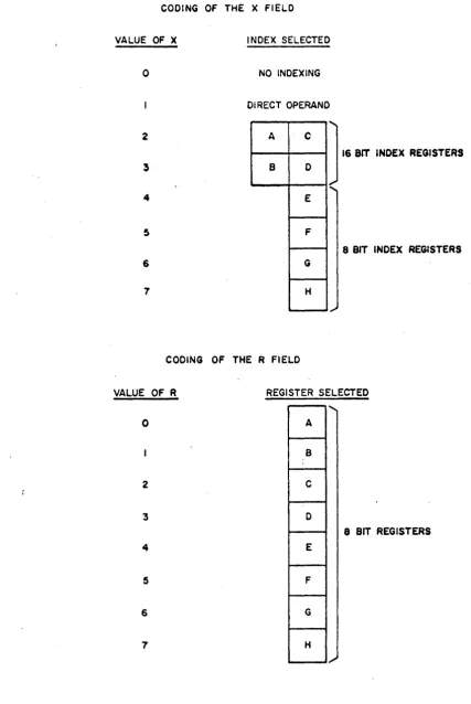
1 3 1 3 16 2Op Code U R I
x
W GU Functions as described for individual instruction, or not used.
R Operand 1 source. R
=
0, 1, ... ,.7: use one of the eight data registers A, B, . . . , H directly.I Operand 2 indirect bit. I
=
0: direct. I=
1: indirect.x
WiG
x
=
0: No indexing.X
=
1 : Use the right-mo st bits of WIc
as a direct operand.X
=
2, 3:
Use l6-bit index registers A, C and B,D.
X
=
4-7: Use 8-bit index registers E, F, G,H.
Ope rand 2 source. Obtain operand 2 from core memory
word location Wand character position G, indexed as speci-fied by X.
Note: Operand 2 is usually referred to as "the
specified character in memory. 11
1. Character Transfer
The following instructions permit single characters of data to
be transferred between the specified data register and the
specified characte r position in core memory.
BBR
BRM
Bring to R
Bring the specified character in memory to registe r R.
Timing: 2 IF X
I
I, I IF X=
IBring to R through Mask
Bring the specified character in memory to register R
through the mask in Register E. Zeros in E inhibit
COOING OF THE X FIELD
VALUE OF X INDEX SELECTED
o
2
3
4
5
6
7
NO INDEXING
01 RECT OPERAND
A C
J
B 0
E F G
H
",.
COOING OF THE R FIELD
16 BIT INDEX REGISTERS
8 BIT· INDEX REGISTERS
VALUE OF R
o
REGISTER SELECTED
2
3
4
5
6
7
A B C 0
8 BIT REGISTERS
E
F
G
H
[image:28.617.93.521.61.700.2]/
Figure 4-1. Register Selection
STR
STM
info rm ation tran sfe r to the co r re sponding bits of R.
Timing: 2 IF X
I
1, 1 IF X=
1Store R
Store the characte r in registe rR into the specified
mem-0ry location.
Timing: 2
Store R through Mask
Store the characte r in regi ste r R into the specified
mem-0ry location through the mask in register E. Zeroes in
E inhibit change in the corresponding bits of the memory
location.
Timing: 2
2. Multiple-Character Transfer
;
, The following instructions permit the simultaneous transfer of
multiple-character groups between certain data registers. They
are useful for rapidly loading or unloading a group of registe r s.
The R field of these commands is utilized as an extension of the
Op Code.
BRL
BRH
STL
Bring to Low Registers
Bring fields CI, C2, C3 andC4 of the specified word in
lTIelTIory to the low registers A, B, C and D respectively.
Timing: 2
Bring to High Registers
Bring fields CI, C2, C3 and C4 of the specified word In
memory to the high registe rs, E, F,. G and H re spectively.
Timing: 2
Store Low Registers
Store the characters in the low registers A, B, C and D
into the specified word in nlernory in fields CI, C2, C3
and C4 respectively.
Timing: 2
STH
BXA
BXB
SXA
SXB
Store High Registers
Store the characters in the high registers E, F, G and
H into the specified word in memory in fields CI, C2,
C3 and C4 re spectively.
Timing: 2
Bring the right-most
16
bits of the specified word inmemory to the data regi ste r pair A, C de signated as
index register 2.
Timing: 2 IF X
f.
1, 1 IF X=
1Bring the right-most
16
bits of the specified word inmemory to the data register pair B, D designated as
index register 3. ..
Timing: 2 IF X
f.
1, 1 IF X = 1Store the data register pair A, C designated as index
register 2 in the right-most portion of the specified
word in memory.
Timing: 2
Store the data register pair B, D designated as index
register 3 in the right-most portion of the specified
word in memory.
Timing: 2
3. Characte r Arithmetic and Compare
The se instructions will pe rform unsigned arithmetic ope rations
on a single 8 - bit field, 0 r will compare the content s of one of the
data registers with a specified character in core memory. All
characters are considered to be magnitudes, and subtraction
underflow will yield a difference in complement form.
ADD Add
Add the specified character in memory to register Rand
put the re sult in re gi ste r R. Ove rflow se t s the ove rflow
memo.
Tim ing: 2 IF X
f.
1, 1 IF X=
1SUB Subtract
CCM
4. Logical
Subtract the characte r in memory from registe r Rand
put the re sult in regi ste r R. Unde rflow sets the ove
r-flow memo.
Timing: 2 IF
XiI,
1 IF-X=
1Compare Characte r to Memory
The character in register R is compared to the specified
character in memory. If the register contents are
greater than memory, the next sequential instruction is
executed. If the two characters are equal, one
instruc-tion is skipped. If the regi'ster contents are less, two
instructions will be skipped.
Timing: 2 IF
XiI,
1 IF X = 1 (add one if skip occurs)The L-l192 logical ope rations enable setting and te sting any
com-bination of bits held in any of the data registers.
EOR
SCH
Exclusive Or
Replace the specified character in memory with its
bit-by-bit exclusive-or with the contents of register R.
Timing: 2
Set Character
Set all selected bits of register R to Qne (U
=
1) or zero (U=
0). Selected bits are those which are masked by corresponding ones in W. (I is not used.)Timing: 1
TSC Test Character
Test all selected bits of register R for value's of one
(U
=
1) or zero (U=
Q},.'
Selected bits are those which are masked by corresponding ones in W. A skip occ:ursif (1) I = 1 and all selected bit_s match U , or if (2) 1=0
and a mismatch exists.
Timing: 1 (add one if skip occurs)
TSP Test Parity
5. Shift
Test all selected bits of register R for parity. Selected
bits are those which are masked by corre sponding one s
in W. A skip occurs if (I) I
=
1 and parity is odd, or(2) I
=
0 and parity is even. (U is not used.) Timing: 1 (add 1 if skip occur s)Single characters may be shifted within any of the data registers.
Shifting may be open or cyclic as specified. The number of ~
places shifted may be modified by an index register. The shift
count (N) is contained in the right-most bits of the instruction.
A maximum of 8 shifts will be made.
SCL
RCL
Shift Character Left
The contents on register R are shifted left the number
<;>f place s specified by N. Bits shifted past the high
order end of the register are lost, and zeros replace
those shifted away from the low order positions.
Timing: (N
-+-
4)+
1Rotate Characte r Left
The contents of register R are shifted left the number
of places specified by N in a cyclic manner. Bits
leaving the high order end of the register are shifted
into the low orde rend.
Timing: (N
-+-
4)+
16.
Index ModifyDXR Decrement Index Register
The contents of the instruction R field (U
=
~), or the contents of the register specified by the R field issubtracted from the index register as specified by X.
If I
=
¢,
the next sequential instruction will always be executed. If I=
1, 'the result of the decrement will betested. If the decrement did not cause the index
regis-ter contents to pass through zero, the next instruction
is taken from the location specified by W. If the index
register did pass through zero, the next sequential
instruction is executed.
Tinling: 1
IXR Inc rement Index Regi ste r
The contents of the R field or the register specified by
R, according to the setting of U, is added to the index
register specified by X. If I
=
,¢, the next sequentialwill be executed. If I
=
1, the re suIts of the inc rement will be compared to WIe
of the instruction. If the index is grieater, or if it overflowed as a result of theincrement, the next sequential instruction will be
executed. Otherwise one instruction will be skipped.
Timing: 1
4.2 VARIABLE FIELD OPERA TIONS
The se instructions facilitate the proce s sing of variable length characte r
fields as required, for example, by me ssage formatting and editing. This
capability is important in those applications providing message switching
on a mix of both synchronous and asynchronous communication channels.
It is also useful in formatting messages for magnetic tape, disc file,
and/or display equipnlent.
Variable field instruction execution permits each of two ope rand
addre sse s to specify independent field locations and lengths, up to a
maxip1um of 16 characters. The addresses of both operands are
sub-ject to normal modification through indexing and indirect addre ssing.
A separate register, designated the Field Operand Address Register
(FOAR), is provided to hold the address and length of the first operand.
The timing for the execution of mo st field instructions is a function of the
number of characters in each operand field (Fl and F 2 ), and to some extent the locations of word boundaries within these fields. If a
recom-plelnent cycle is required, additional time is required.
Variable field arithmetic operations may be perforlned on both binary
and decin1al operands. The sign of each operand is carried in the least
significant characte r field. The se arithmetic ope rations are alge braic
and are executed in the following manner:
Decimal:
The four least significant bits of each character field contain the decimal
digit. Bit 6 of the least significant characte r of each ope rand field con-tains the sign. The remaining bits will be ignored. The addre ss and
field length of operand 1 is in the Field Operand Address Register.
Operand 1 is added to or subtracted fron1 operand 2, whose length and
address is carried in the instruction word. The result of the operation is
stored in place of operand,2. The result of the operation is in true sign
and Inagnitude form. If the result passes through zero, the ten's
comple-ment (recolTIplecomple-menting) of the result is taken. To yield meaningful
results, in the event the operand lengths are not the same, operand 2
must have the greater length.
Binary:
The least significant bit of the least significant character of each ope rand
is c on side re d to be the ope rand sign. Proce s sing is sim ila r to that
de-scribed for decimal operands above, and operand 2 must always have the
greater length.
The instruction format for variable -field ope rations is similar to that
described for the standard single character commands. U and R in the
instruction word, however, specify a field length of up to
16
characters.The following instructions compri se the 1i st of variable field ope rations.
Timing is given in memory cycles.
IFO Initialize Field Ope ration
This instruction sets up the Field Operand Address Register
(-FOAR). U and R are transferred directly to the FOAR.
The W
Ic
field remains in the instruction register until thespecified addre s s rnodification has been completed, at which time
w/c
is transferred to the FOAR. Except for the spe-cial case of the Compare Fields Equal instruction de scribedbelow, the FOAR must be initialized each time before
another variable field operation is performed.
Timing: 1
SF A Store Field Addre s s
AFB
The contents of the FOAR are stored in U, R, and W
Ic
ofthe specified memory location. The R field of the
instruc-tion is a part of the ope rainstruc-tion code.
Timi:f\g: 2
Add Field Binary
The two binary operands whose addresses are specified by
the FOAR (operand 1) and W
Ic
of the instruction (operand 2)are added algebraically.' The results of the addition
occu-pie s the po sit ion of the second ope rand. The re suIt will
carry true sign and magnitude. Overflow will set the
over-flow memo.
Timing: (a) No recomplement cycle: 3.25
+
.75 F2(b) Recomplement cycle: 4
+
F2SFB Subtract Field Binary
The two binary operands whose addresses are specified by
FOAR (operand 1) and W
Ic
of the instruction (operand 2) aresubtracted alge braically. The re suIts of the subtraction
occupie s the position of the second operand. The re suIt
will carry true sign and magnitude. Underflow will cause
the overflow memo to be set.
Timing: (a) No recomplement cycle: 3.25
+
.75 F2(b) Recomplement cycle: 4
+
F2AFD
SFD
CFE
CFM
Add Field Decin1al
The two decimal operands whose addresses are specified by
FOAR and W
Ic
of the instruction are added algebraically.The sum is stored in the location of the second operand, and
carries true sign and magnitude. Overflow will set the
over-flow memo.
Timing: (a) No recolTIplement cycle: 3.25
+
.75 F2(b) ReCOlTIplement cycle: 4
+
F2Subtract Field' Decimal
The two decimal operands whose addresses are specified by
FOAR and W
Ic
of the instruction are subtractedalgebrai-cally. The diffe rence in sto red in the location of the se cond
operand, and carries true sign and magnitude. Underflow
will set the overflow memo.
Timing: (a) No recolTIplement cycle: 3.25
+
.75 F2(b) Recomplement cycle: 4
+
F 2Compar'e Fields Equal
This instruction compare s the two fields whose addre sse s
are specified by FOAR and W
Ic
of the instruction. Thefield lengths are as sumed to be identical and the length
count in FOAR will be ignored. Comparison is on a
bit-by-bit basi s. Equal com'parison cause s the next sequential
instruction to be executed. Unequal comparison will cause
one instruction to be skipped. Since FOAR need not be
initialized before each execution of CFE, automatic indexing
through a table of contiguous entrie s may be achieved
with-out the use of index registe r s.
Timing: (a) No skip: 2. 5
+
5 F 2( b) Ski p: 3. 5
+ .
5 F 2Compare Field ~agnitude s
The operands whose addresses are specified by FOAR and
W
Ic
of the instruction are compared arithmetically withMFM
signs treated as part of the magnitude. If the ope rand
ad-dressed by FOAR is greater than or equal to the operand
specified by W
Ie
of the instruction, the next sequentialin-struction will be executed. If not, one inin-struction will be
skipped. The two operands used with CFM need not have
identical lengths.
Timing: (a) No skip: 2.5
+
.5 F2(b) Skip: 3.5
+
.5 F2Move Field in Memory
The field whose address is specified by FOAR is moved to
the address specified by W
Ic
of the instruction starting in lowe r memory. Reaching the end of the shorter field willte rminate the operation.
Timing: 2.5
+
.5 (F I , F 2 ) min.4.3 FULL WORD OPERATIONS
The word instructions provide full-word (32 bit) transfer, arithmetic,
and logical ope rations.
The format for most of these instructions is as follows:
6 1 3 1 3 16 2
OP CODE U
I .·:· •.. ·· .. · ... ·1
I Xw
I.:: ·
•... ·
... l
The eight character registers A, B, . . . , H are not modified by
word arithmetic. Fields I, X and Ware still employed tp specify the
location of the second operand. Load and Store word instructions use the
one-bit U field to specify one of two one-word registers, Rand Q. A
third but non-addressable register also participates in word operations.
Word operands are 32 bit numbers, with negative numbers represented
in 2' s complement form. The timing for the following word instructions
is given in memory cycles.
WAD
WSB
WMP
WDV
WCM
Word Add
Add the sp'ecified word in memory to R and put the ,re suIt
in memory. Ove rflow sets the ove rflow memo. Q is
unchanged.
Timing: 2
Word Subtract
Subtract the specified word in memory from R and put the
result in memory. Underflow sets the overflow memo.
Q is unchanged.
Timing: 2
Word Multiply
Multiply the specified word in memory by R, and put the most significant half of the product in R and the least
significant half of the product in Q. The sign of the least significant half is made the saIne as that of the most
signi-ficant half.
Timing:
6.
25Word Divide
Divide the specified word in memory into R & Q and put the quotient in Q. The remainder is placed in R in twos com-plement form.
Timing: 10.5
Word Compare
The word in R is compared to the specified word in
mem-ory. If the' register contents are algebraically greater
than the word in memory the next sequential instruction is
execute d. If the two words are equal, one in'struction is
skipped. If.the register contents are less than the word
in memory, two instructions are skipped.
Tim'ing: (a) No skip: 2
(b) Skip: 3
WBR
WST
weD
WSF
WSL
Word Bring
Bring the specified word in memory to register R (U
=
~)or register Q (U
=
1).Timing: 2
Word Store
Store the word in register R (U = ~) or register Q (U
=
1)into the specified memory loea tion.
Timing: 2
Word Complement
Two's complement the contents of the R register.
Timing: 1
Word Shift
Shift the word in register R (U
=
~) or register Q (U=
1)right (I
=
¢)
or left (I=
1), the nUlnber of places specified by the rightmost five bits of the instruction. Signs arenot included, overflow digits are discarded. Indexing of
the number of places shifted may be modified by indexing.
Timing: 1.5
+
.25NWord Shift Long
Shift the combined words in register Rand Q right (I =
¢)
or left (I
=
1), the number of places specified by the right-most six bits of the instruction. Signs are not included,overflow digits are discarded. The number of places
shifted may be modified by indexing.
Timing: 1.5
+
.25N4.4 PROGRAM CONTROL OPERATIONS
NOP No-Operation
Proceed with. next instruction. (Op code field used only.)
Timing: 1
JMP Jump
Take the next instruction from nlemory location W as
modified by X and 1. (R and U are not used.)
Timing: 1
JSL Jump and Store Location
HLT
The location of this instruction plus one are stored in the
memory location specified by W. The next instruction is
taken from location W
+
1. Only the word address inloca-tion W is affected. Remaining positions are left unchanged.
Timing: 2
Halt
Execution of this instruction halts the computer program
by relTIoving the RUN condition. Depressing the PROGRAM
START pushbutton on the operators console restarts the
program with the instruction specified by the program
counte r. (Op code field used only. )
Timing: 1
4.5 INTERNAL CONDITION OPERATIONS
The L-1192 has a number of internal condition in~icators, which may be
te sted and modified.
Inte rrupts
The interrupts are enabled through the use of a mask, which may be stored
anyv.rhere in core memory. The bits within this mask correspond to the
various interrupt conditions. By enabling interrupts from this mask, only
the desired interrupts may be used.
ESI Enable System Interrupts
The word at location W is used as a mask to enable
inter-rupt operation for the I/O Interface specified by R, U.
For eve ry po sition which contains a one, the c orre sponding
interrupt will be enabled. For every position which
con-tains a zero, the corre sponding interrupt will be disabled.
Timing: 2
System Conditions
System conditions may be set or reset, and tested for on or off condition.
The available instructions utilize the W
Ic
field to select the memo orcondition to be set or tested. This memo or condition is therefore
sub-ject to index register modification.
SSC Set System Condition
TCC
For tho se conditions which can be switched by program,
this instruction will cause the state of the addre s sed device
to be equal to the status of the U bit. Thus, if the U bit is
ze ro, the device will be re se t. If U is one, the devi ce will
be set. If this instruction is addressed to a device which
is not program s~ttable, it will execute as NOP.
Timing: 1
Te st Control Condition
The condition of the specified memo or switch is compared
to the U bit. If the condition and the bit are equal, the
next sequential instruction will be executed. If not equal,
one instruction will, be skipped.
Timing: 1
4.6 COMMUNICATION INTERFACE OPERATIONS
Input-output character transfers for the cOlnm1.1nication channels and the
slow-speed on line devices (paper tape, punched card, and typewriter/
printer) provide interlaced core memory access to permit simultaneous
operation.
Due to frequency of servicing the DDL interface, instructions are
pro-vided which greatly reduce the proce ssing load when removing data froln
the low and high priority channel activity table s (CAT 1, CAT 2). In a
single instruction are com bined the functions of te sting for the pre sence of
data in CAT 1 or CA T 2, bringing the next entry to be proce s sed to the
data registers if data is waiting to be proce ssed, and moving hardware
bookkeeping markel's to the next entry to be processed.
When either ICH or ICL is executed, the relative positions of the load and
unload n1arkers are tested. If the saIne, indicating the tested table is
empty, the instruction terminates and the next sequential instruction is
executed. If the markers are not the same, the entry at the location of
the unload marker (UI, U2) is brought into the data registers as shown:
Character
Channel Idenqty
I/O Indicator
E Register
F Register
G Register
The unload marker is then stepped cyclicly to the next entry position in
the table. The next se quential instruction is skipped and thi s in struction
is terminated.
The format for the ICH and the ICL instructions is:
6 24
Op Code
"
'. ". . .. :" . ': .. : ", . . ":, .: ':T;· ,"', . '. .... .: )/(\
.:.;.:.'~.:-.'.
: ....•... :.::: :.'.::.'. : .•. :.:", ::.: ... :.::.::: .. :.:.: ... :.: ... : .. :: .. :.: ...:.~
.. :.:.: .. : •... :, ... : ...•.. :.:.: .. : ... : ...• : •... : ... ,"'~('
... ," . .'. ",. . . '.. . ." .'. ... . . :., :,'. . :j:'::::::: /(:}/:.:.: •. '" .'.
:.:::
..'::]
ICH Initiate High Priority Character Cycle
The relative positions of Ll and DI are tested. If equal,
the current instruction terminates and the next instruction
in sequence is executed. If not identical, the next entry
in CAT 1 is obtained from the location specified by Dl.
The next sequential instruction is skipped and Dl is
automatically stepped.
Timing: 1 IF LI
=
DI, 2 IF LlI-
Dl ICL Initiate Low Priority Character CycleThe relative positions of L2 and U2 are tested. If equal,
the current instruction te rminate s and the next sequential
instruction is executed. If unequal, the next entry is
acce ssed from CA T 2 at the location specified by U2.
U2 is stepped, the following instruction is skipped, and
the current instruction is terminated.
Timing: 1 IF ,L2 = U2, 2 IF L2
I
U2The ECH and the DCH instructions control the operation of the DDL
inter-face, module scanner. The instruction format is:
ECH
DCH
6 1 3 22
Op Code
II
REnable Channel
The interface module attached to scanner position R
(one of eight positions) is placed in operation.
Charac-te r s will be automatically input or output unde r control
of the Line Unit Interface module or Low Speed I/O device.
Timing: 1
Disable Channel
The interface module attached to scanner position R (one
of eight positions) i$ taken out of operation. Any fragment
of a character in transmission will be lost.
Timing: 1
4.7 INPUT/OUTPUT OPERATIONS
The L-1192 Controller Processor may interface with up to sixteen I/O
Channels. Each channel added to the system contains the required
con-trol logic plus a Command Regi ste r and a Block Concon-trol Regi ste r, and
can communicate with up to 16 peripheral devices.
For the purpose of the following discussion, the term "instruction" refers
to those operations which are decoded and executed in the instruction
register. The term "command" designates those operations which are
executed in the I/O interface. To activate most input/output operations,
it is necessary for the L-1192 program to initiate