(
+---+---+---+---+---+
IHONEYWELL INFORMATIONI SPEC. NO. SHEET IREVISIONI
I SYSTEMS ITALIA I I I
I I A78xxxxxx 1/62 I DRAFT 1 I
+---+---+---+---+--~---+
I Prepared by Date Designation
1 1
I P. GONELLA 86.05.071
+---+
I Approved by Date
1 1
PRODUCT DESIGN DESCRIPTION
s.
G. M. 2LIN E PRO C E S S 0 R 0
+---+---+
REVISION RECORD
REV AUTHOR I TY DATE APPROVED BY SHEETS AFFECTED
ALL
-****
****
***
*****
*****
* *
* *
* *
*
*
* *
*
*
* *
*
*
* *
****
*****
****
*
* *
*
*
*
*
*
*
* *
* *
* *
*
*
****
* *
*
*
*
*
This document and the Informatlon contalned hereIn are confldentlal to and the property of Honeywel I Information Systems, Inc. and are made
available only to Honeywell employees for the sole purpose of
conducting Honeywell's business or provIding goods and services to
Honeywel I. This document, any copy thereof and the InformatIon
conta I ned here
r
n sha I I be ma I nta I ned In str I ctest con f I dence; sha I I not be copIed In whole or In part except as authorlzed by the Honeywel I employee's manager or by an authorIzed Honeywel I offIcIal In wrltlng; and shall not be dIsclosed or dlstrlbuted (a) to persons who are not Honeywell or vendor employees, or (b) to Honeywell or vendor amp loyees for whom such l n format l on I s not necessary I n connect Ion wIth theIr assIgned responsIbIlItIes. Upon request, or when the Honeywe I I emp loyee or vendor I n possess lon of th I s document no 'Ionger has need for the document for the author I zed Honeywe I I purpose, th I s document and any cop t es thereof sha I I be returned to the Honeywe II employee's manager or to Honeywell. There shall be no exceptIons to the terms and condItIons set forth hereIn except as authorIzed In(-~
c
IHONEYWELL INFORMATIONI I SPEC. NO.1 SHEET lREVISIONI SYSTEMS I TALI A 1 LI NE PROCESSOR 0 1 1 1 1
P.D.D. I A78xxxxxx 1 2 1 DRAFTl 1
+---+---+---+---+---+
1 1 • 1 1 • 1 • 1 1.1.2 1 .1 .3 1.1.3.1 1.1.3.2 1.1.4 1.1 .5 1 .1.6 1.1.7
2
3
INDEX
GENERAL DESCRIPTION HARDWARE DESCRIPTION
I/O MICROPROCESSOR AND DMA EMULATOR MASTER AND SLAVE INT & INTA LOGIC SERIAL INPUT OUTPUT
CONFIGURATION
ELECTRICAL INTERFACE AND MODEM SIGNALS TIMER and PARALLEL PRINTER INTERFACE VME BUS INTERRUPTER LOGIC
ATTENTION LOGIC
PROCESSOR NUMBER AND BOARD TYPE DETECTION
DMA EMULATOR INTERFACE
c
IHONEYWELL INFORMATIONI I SPEC. NO. I SHEET IREVISIONI
I I I I
I SYSTEMS ITALIA LINE PROCESSOR 0
I P.D.D. I A78xxxxxx I 3 I DRAFT1 I
+---+---+---+---.+---+
1. GENERAL DESCRIPTION
The 1ine frocessor 0 is an intellIgent communicatIon processor with SGM2-VME bus Interface, wh tch supports up to 6 fu II dup I ex channels with RS-232C and RS-422A Interfaces, for serIal communicatIons and one CentronIcs/IBM paral lei prInter Interface.
In VME env I roment the LIne Processor 0 I s a s I ave contro I I er fu I I Y compat Ib Ie wh ich responds to 32-b It addressing and 8 or 16 b it data transfers. CommunIcatIons between the system CPUs and the LPO can take place In three ways:
from host to LPO or vice versa by message I nterchange v I a a shared-RAM allocated on the LPO;
from host to LPO by wrftlng an 1-blt attentIon regIster to Interrupt the LPO;
from LPO to host by an Interrupter that generates Interrupts to the VME bus on any of the seven levels and supplIes an 8-blt vector durIng Interrupt acknowledge cycle. The request level and the vector are programmable by the local processor.
The memory of the LP cons I sts of 32Kbytes EPROM area, 512Kbytes of Loca I D I nam' c Memory, 64Kbytes of Shared Sram Memory and 16Kbytes of
('"
c
+---+---+---+---~---+
lHONEYWELL INFORMATIONI I SPEC. NO. I SHEET IREVISIONI
I SYSTEMS ITALIA I LINE PROCESSOR 0 1 I I I
I I P.D.D. I A78xxxxxx I 4 I DRAFT 1 I
+---+---+---+---~+---+
1 .1 HARDWARE DESCRIPTION
The Major Block Diagram of the LINE Processor 0 board Is descrIbed In details In FIg. 1.1 where It Is possible to see the following functional areas:
- the local area;
- the I/O area;
- the shared area;
The maIn functIonal blocks are:
- MICROPROCESSORS AND DMA EMULATOR
the mIcroprocessors used are the 16 bIt Motoro I a MC68000. They operate at 12.5 Mhz clock and they have an addressing capabilIty up to 16 Mbytes (see para. 1.1.1); In th
r
s board oner
s master, the other Is slave and It emulates a DMA.- MA$TER AND SLAVE INT & INTA LOGIC
thIs logic permits to handle the Interrupt lInes (see para.
1.1.2.);
NOT I FY . INTERRUPTS.
by this logic the slave processor can Interrupt the master processor and vlceversa. (see para. 1.1.2);
- CHIP SELECT AND CONTROL LOGIC FOR I/O, LOCAL AND SHARED AREA
the main functions carried out by this logic are the fol lowing:
- generation of the chip-selects;
- generat Ion of contro I signa Is (for examp I e, the READ and WRITE clocks of the memory, etc);
- generation of DATA TRANSFER ACKNOWLEDGE signal 'towards MC68000;
{
+-tT--,-
---IHONEYWELL INFORMATIONI I SPEC. NO. I SHEET IREVISIONI
SYSTEMS I TALI A I LINE PROCESSOR 0 I I I I
P.D.D. I A78xxxxxx I 5 I DRAFT1 I
+---+---+---+---~+---+
LINE PROCESSOR 0 - MASTER PROCESSOR MEMORY MAP
SYSTEM BUS VME BUS
*
FF.FF.FF 1---1
1 RFU 1 256 Kbytes
Fe.DO.DO 1---1
ATIENTION LOGIC
F8.00.00 1---1 ---56.38.00.00
RESET SYSTEM FAIL
F4.00.00 1---1 ---56.34.00.00
RFU
FO.OO.OO 1---1
RFU
EC.OO.OO 1---1
IGOR
EB.OO.OO 1---1
RFU
EO.DO.CO I---t
RFU
08.00.00 1---1 1
1 RFU
! 1
DO.OO.OO 1---1
1 1
1 RFU 1
1 1
C8.00.00
1---1
---56.08.00.001 I
1 SHARED SRAM 512 Kbytes
1 1 I
CO.OO.OO !---1 ---56.00.00.00
-
+---+---+---+---~---T
IHONEYWELL INFORMATIONI I SPEC. NO. I SHEET IREVISIONI
SYSTEMS I TALI A I LI NE PROCESSOR 0 I I I I
I P.D.D. I A78xxxxxx I 6 I DRAFT 1 I
+---+---+---+---+---+
i (
1---1
BF.FF.FF 1
I PIT
1 1
BB.OO.OO
1---1
1 1
1 RFU I
I 1
BO.OO.OO 1---1
I 1
I PROCESSOR NUMBER REGISTER 1
1 I
AB.OO.OO
1---1
IWRITE NOTIFY VECTOR REGISTERl
A4.00.00
1---1
1 READ I/O TERM.VECT.REG
AO.DO.CO 1---1
RFU
(
98.00.001---1
1
1 RFU
I 1
90.00.00
1---1
1 1
I RFU 1
1 1
88.00.00
1---1
RFU
IHONEYWELL INFORMATIONI SPEC. NO. I SHEET IREVISIONI
I SYSTEMS ITALIA LINE PROCESSOR 0 I I I
I P.D.D. A78xxxxxx I 7 I DRAFT 1 I
+---+---+---+---+---+
1---1
7F.FF.FF MODEM 0 REGISTER OUT
7C.OO.OO 1---1
MODEM 1 REGISTER OUT
78.00.00 1---1
MODEM 0-1 REGISTER IN
74.00.00 1---1
RFU
70.00.00 1---1
WRITE 1/0 TERM. REG.
6C.OO.OO 1---1
READ NOTIFY VEC. REG.
68.00.00 1---1
RFU
60.00.00 1---1
RFU
58.00.01 1---1
S I 02 LI NES 4-5
50.00.01 1---1
1
1 SI01 LINES 2-3
I 1
48.00.01
1---1
1 !
1 SIOO LINES 0-1 !
! 1
c
• -- ---- - - I - - - .
IHONEYWELL INFORMATIONI SPEC. NO. ( SHEET (REVISIONI
I SYSTEMS ITALIA LINE PROCESSOR 0 ( I I
I P.D.D. A78xxx>o<x ( 8 I DRAFT1 I
+---+---+---+---+---+
3F.FF.FF
1---1
RFU 1 1
1
38.00.01 I---J
RFU
30.00.00 1---1
1/0 SRAM
28.00.00 1---1
RFU
20.00.00 1---1
18.00.00
RFU
1---1
11 I
RFU
10.00.00 1---1
LOCAL DRAM
08.00.00 1---1
LOCAL DRAM
00.00.00 1---1
I
c
·---T---T---~---T
IHONEYWELL INFORMATIONI I SPEC. NO. , SHEET IREVISION'
SYSTEMS ITALIA 'LINE PROCESSOR 0 I " I
, P.D.D. I A78xxxxxx I 9 I DRAFT1 ,
+---+---+---+---.+---+
LINE PROCESSOR 0 - SLAVE PROCESSOR MEMORY MAP
'SYSTEM BUS VME BUS
*
FF.FF.FF 1---1
RFU 256 Kbytes
Fe.co.co 1---1
ATIENTION LOGICFB.CO.OO 1---1 ---56.38.00.00
RESET SYSTEM FAILF4.00.00 1---1 ---56.34.00.00 RFU
FO.OO.CO 1---1
RFU
EC.OO.OO
1---1
IGOR
EB.OO.OO 1---1
RFU
EO.CO.OO 1---1
RFU
08.00.00 1---1
. I
RFU
00.00.00 1---1
RFU
CB.OO.OO 1---1 ---56.0B.00.00
,
SHARED SRAM 512 Kbytes
I
CO.CO.CO 1---1 ---56.00.00.00
-
(
c
- - - -- -- • ----~---I - - - • IHONEYWELL INFORMATIONI
I SYSTEMS ITALIA LINE PROCESSOR
a
I I SPEC. NO. I SHEET IREVISIONI I I II P.D.D. I A78xxxxxx I 10 I DRAFTl I
+---+---+---+---~+---+
1---1
BF.FF.FF 1
! PIT
1 1
B8.00.00
1---1
1 1
1 RFU 1
1 1
BO.OO.OO 1---1
1 1
1 PROCESSOR NUMBER REGISTER 1
1 1
AS.CO.DO 1---1
IWRITE NOTIFY VECTOR REGISTER!
A4.00.00 1---1
I READ 1/0 TERM.VECT.REG
AO.DO.DO 1---1
RFU
98.00.00 1---1
RFU
90.00.00 1---1
LOCAL DRAM
88.00.00 1---1
LOCAL DRAM
IHONEYWELL INFORMATIONI SPEC. NO. SHEET IREVISIONI
I SYSTEMS ITALIA LINE PROCESSOR 0 I I
I P.D.D. A78xxxxxx 11 I DRAFT1 I
+---+---+---+---~+---+
(
.... ~ ,1---1
7F.FF.FF MODEM 0 REGISTER OUT
7C.OO.OO 1---1
MODEM 1 REGISTER OUT
78.00.00 1---1
MODEM 0-1 REGISTER IN
74.00.00 1---1
RFU
70.00.00 J---I
WRITE 1/0 TERM. REG.
6C.OO.OO 1---1
READ NOTIFY VEC. REG.
68.00.00 1---1
RFU
60.00.00 1---1
RFU
(
58.00.01 1---1SI02 LINES 4-5
50.00.01 1---1
1
1 SI01 LINES 2-3
1 1
48.00.01 1---1
1 1
1 SIOO LINES 0-1 1
1 1
40.00.01 1---1
C.·'.-·'
,T---+---+---+---+
lHONEYWELL INFORMATIONI I SPEC. NO. I SHEET IREVISIONI I SYSTEMS I TAL I A I LINE PROCESSOR 0 l I I I
I I P.D.D. I A78xxxxxx I 12 I DRAFT1 I
+---+---+---+---+---+
1---1
3F.FF.FF
RFU
38.00.01 1---1
RFU
30.00.00 1---1
1/0 SRAM
28.00.00 1---1
RFU
20.00.00 1---1
RFU
18.00.00 I---J
RFU
10.00.00 1---1
. I
EPROM I
I 08.00.00 1---1
. EPROM
00.00.00 1---1
I
512 KByte
c
- - - I - - - , ---r-'~ .-~,--.
IHONEYWELL INFORMATIONI I SPEC. NO. I SHEET IREVISIONI
I I I I
I A7Bxxxxxx I 13 I DRAFT1 I
I SYSTEMS ITALIA LINE PROCESSOR 0
I P.D.D.
+---+---+---+---~+---+
- ONBOARD/VME DECODE
th I slog I c carr I es out the shared-b us req uests to th e BUSCON when either the loca I processor or the system CPUs want to transfer data Into shared memory, or attention register, or BIL;
- I/O MEMORY
The 1/0 memory consists of 2 BxBKbytes static ram connected in such a way that It constitutes one BKword bank.
It Is mapped in the fol lowing address range:
- OB Kwords bank: 2B.00.00 Hex --> 2B.3F.FF Hex.
- EPROM
I n the 110 area we find the EPROMS, two 16 Kbytes packages (Eprom 2712B) have been used. These two packages are connected in such a way that they constitute one 16 Kwords bank; the required access time is 200 ns which allows the dialogues to be carried out with one wait cycle. The BKwords/16Kwords EPROM bank
Is mapped in the fol lowing address range of the slave 6BOOO:
- 16 Kwords bank: 00.00.00 Hex --> 00.7F.FF Hex.
The Eprom code carries out the fol lowing functions:
- Exception Vector Table;
- Resident DiagnostIc RoutInes;
- H/W initialization of the whole LPO board;
- LOCAL MEMORY
the loca I memory cons I sts of 16 256K x1 DRAM packages p I us two 256K x1 DRAM packages ut i I I zed I I ke check bit. The 256K x1 packages are connected in such that they constitute one 256 Kwords bank. This memory can be accessed at byte length (right byte and left byte) and at word length with zero or maximum one walt cycles.
The LOCAL MEMORY bank is mapped, for the slave processor, In the following address range:
c
- ---.,-~~--...
-+---+---+---+---+
IHONEYWELL INFORMATIONI SPEC. NO. SHEET IREVISIONI
I SYSTEMS ITALIA I LINE PROCESSOR 0 I I
I P.D.D. A78xxxxxx 14 I DRAFT1 I
+---+---+---+---+---+
On the other hand, the master processor sees the local memory In the fol lowing address range:
00.00.00 Hex --> 07.FF.FF
When an error occurs In the Local Memory, the check logic sets the 68000 In the HALT state and asserts the VME SYSFAIL signal. SYSFAIL condition can be removed under Operating System control writing or reading ( byte or word length) the RESET SYSTEM FAIL flip/flop located at the fol lowing address:
F4.00.00 Hex for the system bus
56.34.00.00 Hex for the VME bus (first processor . number)
The d I agnost I cs can generate an I nverted memory check bit to test the error detection circuit. For this feature the PC4 Port C bIt of the Para I leI Interface Timer has been used.
Writing a 0 into the PC4 bit of the PIT the Inversion of the check bit will be generated. For The Port C Addressing space, refer to figure 1.1.4.3. (MC68230 Register Model).
- SERIAL INPUT OUTPUT
three USART (SIO) have been used. Each of these controllers can handle two SerIal Ports (see para 1.1.3);
- PARALLEL INTERFACE TIMER (PIT)
It Is a logIc which permIts to send sIngle or perIodIc
programmab I e I nterrupts to the MC68000 microprocessor and to connect the prInters having an IBM and CENTRONICS type parallel
Interface (see para. 1.1.4). PIT Is also utJlIzed for diagnostics purpouses, notify Interrupts and It Is located In the local area;
- VME BUS CONTROLLER (BUSCON)
(
C',"'\
... '+---+---..:~.::;.:..::;.:::----+-.::;.~~~---+---+
IHONEYWELL INFORMATIONI SPEC. NO. SHEET IREVISIONI
I SYSTEMS ITALIA I LINE PROCESSOR 0 I I
I I . P.D.D. A78xxxxxx 15 I DRAFT 1 I
+---+---+---+---+---+
- SHARED MEMORY
the shared memory consIsts of eIght 8Kx8 SRAM packages plus two 64Kx1 SRAM packages utI I Ized I Ike check bIt. The 64 Kbytes packages are connected In such a way to constItute one 32 Kwords bank. ThIs memory can be accessed at byte length (rIght byte and
left byte) and at word length wIth at least four walt cycles.
The SHARED MEMORY bank Is mapped In the fol lowIng address range:
CO.OO.OO Hex --> CO.FF.FF Hex;
When an error occurs I n the Shared Memory, the check log I g asserts the BUS ERROR signa I to the processor that I s read I ng the memory.
The d I agnost I cs can generate an I nverted memory check bIt to test the error detectIon circuit. For this feature the PC4 Port C bit of the Paral lei Interface Timer has been used.
Writing a 0 Into the PC4 bit of the PIT the inversion of the check bit will be generated. For The Port C Addressing space, refer to figure 1.1.4.3. (MC68230 Register ModeJ).
- VME BUS INTERRUPTER LOGIC
this logic acts as an interrupt requester on VMEbus (see
para.1.1.5);
- ATTENTION LOGIC AND SYSTEM FAIL DETECTION
this logic permIts the system CPUs to Interrupt the LP and, in case of LPO system fail, to recognize the system fail condition of the board (see para. 1.1.6);
- PROCESSOR NUMBER AND BOARD TYPE DETECTION
thIs logic allows to recognIze In which slot of the VME bus the board was inserted to confIgure the lines.
6
z ~ =e: rnr-8
z 'TI o rn ~ > r->e
""0 ~ ""0 :::0 ~~
~
'TI (Q --•...
I'V.H~R_.uP ~ " I
6~
(A
)f'J----;,lf--:...,-
.. : :
-1HT, itA., J-t ---~ 8R-§G-M.AC):,-0
?p ~-~~~----~~~
,e0e0(~)
rn.
l
,~
.
SGM? - LINE COMMUI~ICATION PROCESSOR LP0
MAJOf\ BLOCK OfAGfiAM
LOCAL DA.TA BUS
- - , ' _ _ ...J
6 5 5
1)
11
1'1;
i
'WIA'li!
r./o M'E-MORoY 8 KWORJ)" 510 685(;4h rIT
68230
1 ,
... .
IHf" UnA
SIGHAlS fOil
I/O O[VICES
,
z.?J2./422.
.DRI~€la
Re.:!~
7l
#-2 -reRMIIj,ALS -12.
II
LOCJ,ttiNe'S #2 C:OMMUNICATION
LINES
~
'\ ~,c1illl IIEa«
r
'IDUSCON 6617Z
'
-,
o
t -
- - + z1 •
I I
r-z rn
""0""0
• :::0
0 0 · n orn
• en en o ::0 o 1 1 + - - - - +
1 1
I > enl
I ... "'01
10) rnl
1 X n 1
1 X • 1
I X 1
1 X Z I
1 X 0 1
1 X . ,
1 ,
+ - - - + I
,
,
,
....
,0\
,
I .
en :r rn rn -f
+----I :::0
'0
rn 1:::0 < )' »''TI en
l - f
, 0
, Z
c~
C
----.---.---T---T
IHONEYWELL INFORMATIONI SPEC. NO. SHEET IREVISIONI
I SYSTEMS ITALIA LINE PROCESSOR 0 I I
I P.D.D. A78xxxxxx 17 I DRAFT1 I
+---+---+---+---~+---+
1.1.1 MICROPROCESSORS AND DMA EMULATOR
The LPO uses two Motorola "MC68000 16-BIT MICROPROCESSOR" with a 12.5 Mhz frequency clock.
The main characteristics of this microprocessor are the fol lowing:
- 64 pins Microprocessor;
- 16 bits Data Bus;
- 24 bits Address Bus;
- 16 Megabytes which are directly addressable;
- I/O mapped In memory;
- 17 Internal 32 bIts regIsters;
- 32 bIts Program Counter;
- 16 bIts Status Register;
- 56 dIfferent types of Instructions;
- operatIon at BITs, DIGITs, BYTEs (8 bytes) WORDs (16
bIts) LONG WORDs (32 bits) length;
- two prlviliged statuses: SUPERVISOR status and USER
status.
The two microprocessors share the same bus and memor
r
es and can communicate each other by the NOTIFY INTERRUPT and the TERMINATION I/OINTERRUPT (see para. 1.1.2).
At the InitIal time the master Is In HALT state until the slave Initializes the LPO board. When the slave processor finishes Its job, (It prepares exceptIon tables, It down-loads programs In the local and I/O memory from shared memory, etc.), It wakes up the master wrIting a logIc zero In the PC2 bit of the PIT Port C. (see para.1.1.4).
Thus the master leaves Its halt state and starts Its routine whl Ie the slave keeps on waiting for commands from the master. <
I t i s to be noted that, when needed, both microprocessors can have access to the all shared resources, but the access Is much faster to the HW resources connected to Its bus. For instance:
Master 68000 access to LOCAL MEMORY in 400 ns.
I/O MEMORY In 560 ns.
SHARED MEMORY in 640 ns.
Slave 68000 access to LOCAL MEMORY In 560 ns.
I/O MEMORY in 320 ns.
c
c
IMVNcTWcLL IN~URMATIONI
I SYSTEMS ITALIA I
I I
.. -~"-rSPEC.NO~ -rSi.fEET-~TRE~T--"
LINE PROCESSOR 0 I I I I
P.D.D. I A78xxxxxx I 18 I DRAFT 1 I
+---+---+---+---~+---+
If the MASTER processor wants to read or write the I/O memory and at the same time, the SLAVE processor wants to have an access to the LOCAL MEMORY, the MASTER processor re-runs the last Instruction after the end of the slave access In the LOCAL MEMORY.
In case of TAS InstructIon on the I/O memory by the MASTER processor during the same condItion upon described, the master will not re-run the I nstruct Ion, but a BUS ERROR w I I I happen. A software treatment of this BUS ERROR must be done.
(
.---T---T---+---+
IHONEYWELL INFORMATIONI
I SYSTEMS ITALIA LINE PROCESSOR 0
I P.D.D •.
I SPEC. NO. I SHEET lREVISIONI
I I I I
I A78xxxxxx I 19 I DRAFT1 I
+---+---+---+---+---+
1.1.2 MASTER AND SLAVE INT & INTA LOGIC
The iNT & INTA LOGIC carries out the fol lowing functions:
- It receives the Interrupt signals;
- It handles the Interrupt priorities;
- It notIfIes to the MC68000 the Interrupts with the highest
priority by coding the three lines, IPLO, IPL1, IPL2
(Interrupt Control);
- It acknowledges and handles the Interrupt Acknowledge cycle using FCO, FC1, FC2 lines (Processor Status) and the A1, A2, A3 address signals.
C'
(
0
,~~~---T---T---T---+ IHONEYWELL INFORMATIONI
I SYSTEMS ITALIA I LINE PROCESSOR 0
I I P.D.D.
I SPEC. NO. I SHEET IREVISIONI
I I I I
I A78xxxxxx I 20 I DRAFTl I +---~--+---+---+---+---+
The master handles the following Interrupts:
Level Interrupt
+ with the highest prIority
7 (NMI) NOT USED
/ ( Special RX Cond.
I ( RX Data Request I LI NE'2 < TX Data Request I ( STS CHG Request SIOl I
I ( Special RX Cond. I LINE'3 < RX Data Request
I ( TX Data Request I ( STS CHG Request I
I ( Special RX Cond.
I ( RX Data Request
I LINE'O < TX Data Request I ( STS CHG Request
6 SIOs SIOO <
I ( Special RX Cond. I LI NE'l < RX Data Request I ( TX Data Request
I ( STS CHG Request I
I ( Special RX Cond.
I ( RX Data Request I LINE'4 < TX Data Request I ( STS CHG Request SI02 I
I ( Special RX Cond. I LINE'5 < RX Data Request I ( TX Data Request I ( STS CHG Request
\
5 NOT USED
4 INTERRUPT FROM DMA EMULATOR (SLAVE PROCESSOR)
3 TIMER
2 ATTENTION REGISTER
1 PARALLEL PRINTER
c
+---+---+---+---T
IHONEYWELL INFORMATIONI \ SPEC. NO. I SHEET lREVISION\ \ SYSTEMS ITALIA \ LINE PROCESSOR 0 \ \ \ \
\ P.D.D. \ A78xxxxxx \ 21 I DRAFT1 I
+---+---+---+---~+---+
When the SLAVE needs to commun Teate with the MASTER processor It must write the Interrupt vector In the 1/0 TERMINATION REGISTER
located at:
and Hex 6c.oo.01 for the write cycle Hex Ao.00.01 for the read cycle
Then wrItIng a zero In the PCO bIt of the PIt Port C, It gives Interrupt to the master at fourth level.
The right flow of the SLAVE operations Is:
1) Test until the PCO bIt Is set to one from the MASTER processor (NO INTERRUPT PENDING).
2) When the PCO I s one, write the I nterrupt vector on the I/O TERMINATION REGISTER.
C'
(-·---T---r---T-~---"''''''T·' IHONEYWELL INFORMATIONI
I SYSTEMS ITALIA I LINE PROCESSOR 0
I
J
P.D.D.I SPEC. NO. I SHEET IREVISIONI
I I I I
I A78xxxxxx I 22 I DRAFT1 I
+---+---+---+---~+---.--+
On the contrary, the slave processor handles the followIng Interrrupts:
Level Interrupt
+ wIth the hIghest prIority
7 (NMI) NOT USED
6 NOT USED
/ •
I { RXRDY DMA signal
I 1I NE'2 <
I { TXRDY DMA signal SI01 I
I ( RXRDY DMA signal I lINE#3 <
I ( TXRDY DMA signal I
5 SIOs <
I
I
I ( RXRDY DMA signal
I LINE'O <
I ( TXRDY DMA signal SIOO I
I ( RXRDY DMA signal I LINE'1 <
I ( TXRDY DMA signal \
4 NOT USED
3 NOT USED
2 NOT USED
NOTIFY INTERRUPT
(
---.---T---+
IHONEYWELL INFORMATIONI SPEC. NO. SHEET IREVISIONI
SYSTEMS ITALIA I LINE PROCESSOR 0 I I
I P.D.D. A78xxxxxx 23 I DRAFT1 I
+---+---+---+---+---+
The S i os interrupt the s I ave processor us i ng the TXRDY and RXRDY pins connected to a priority encoder that gives the following priority to each I ine (from highest to lowest):
Line 2 Receive Ready
Line 2 Transmit Ready
Line 3 Receive Ready
Line 3 Transmit Ready
Line 0 Receive Ready
Line 0 Transmit Ready
Line 1 Receive Ready
Line 1 Transmit Ready
The interrupt vector is automatically generated by a logrc that provides different interrupt vectors:
Hex 40 for Line 2 Receive Ready Interrupt
Hex 41 for Line 2 Transmit Ready interrupt
Hex 42 for Line 3 Receive Ready interrupt
Hex 43 for Line 3 Transmit Ready Interrupt
Hex 44 for Line 0 Receive Ready i-nterrupt
Hex 45 for Line 0 Transmit Ready Interrupt
Hex 46 for Line Receive Ready interrupt
Hex 47 for Line Transmit Ready Interrupt
(
---.---T---T
IHONEYWELL INFORMATIONI SPEC. NO. SHEET IREVISIONI
SYSTEMS ITALIA I LINE PROCESSOR 0 I I
P.D.D. A78xxxxxx 24 I DRAFTl I
+---+---+---+---~+---+
The master processor to interrupt the slave, must
interrupt vector in the NOTIFY REGISTER located at: write the
Hex A4.00.03 for the write cycle and
Hex 68.00.01 for the read cycle
Then writing a zero In the PCl bit of the PIT Port C It Interrupts the slave processor.
The right flow of the MASTER operations Is:
·1) Test unt II the PCl b It I s set to one from the SLAVE processor (NO INTERRUPT PENDING).
2) When the PCl Is one, write the Interrupt vector on the NOTIFY REGISTER.
3) Write a zero In the PCl bit of the Pit Port C (INTERRUPT TO THE SLAVE).
When an Interrupt Is acknowledged by the MC68000 microprocessor an "INTERRUPT ACKNOWLEDGE" cycle Is performed and the INT
&
INTA LOGIC activates the Interrupting device which responds by sending one VECTOR(byte) on the Lower Data Bus.
Th is vector I s then I atched and used by the MC68000 to se I ect one of the 256 possible pointers of the Exception Vector Table located I n Eprom for the s I ave microprocessor and I n I oca I DRAM for the master.
<.
c\
---T---+---+---+
IHONEYWELL INFORMATIONI SPEC. NO. SHEET IREVISIONI
I SYSTEMS ITALIA I I I
I I
LI NE PROCESSOR 0
P.D.D. A78xxxxxx 25 I DRAFT1 I
+---+---+---+---+---+
1.1 .3 SERIAL INPUT OUTPUT
The LPO serIal ports al low Local and Remote Asynchronous
CommunIcatIons and Local and Remote Synchronous communicatIon by means of RS-232C (V24/V28) and RS-422A (Vl1) electrIcal Interface.
The handlIng of the serIal ports are made by the SerIal Input Output (SIO) 68564 whIch are LSI chIps wIth 48 pIns dual In lIne packages operatIng at 5 Mhz clock.
TheIr maIn characterIstics are the fol lowIng:
- compatible wIth MC68000;
- two independent ful I-duplex channels;
- dIrect I y addressab I e reg I sters (a I I contro I reg I ster are read/wrIte) ;
- receIve data regIsters are quadruply buffered, transmIt regIsters are doubly buffered;;
- Self-test capabi lity;
- Dma pIns;
- daIsy chaIn priority interrupt logIc provides automatic Interrupt vectorIng without external logic;
- Asynchronous features:
*
5,6,7 or 8 bits/character*
1,1/2 or 2 stop bIts*
even, odd or no parIty*
xl, x16, x32 and x64 clock modes*
break generatIon and detectIon*
parity, overrun and framing error detectIon- Byte Synchronous features:
*
Internal or external character synchronIzation;*
one or two sync characters In separate regIsters;*
automatIc sync characters insertion;*
CRC 16 or CRC-CCITT block check generation and checkIng;- BIt synchronous features:;
*
abort sequence generation and detection;*
automatic zero insertIon and detection;*
automatic flag InsertIon between messages;*
address fIeld recognition;*
I-field residue handling;*
valid receive messages protected from overrun;c:
(
.---T---+---+---~---+
IHONEYWELL INFORMATIONI I SPEC. NO. I SHEET IREVISIONI
I I I I
I A78xxxxxx I 26 I DRAFT1 I
I SYSTEMS ITALIA I LINE PROCESSOR 0
I P.D.D.
+---+---+---+---.+---+
1.1.3.1 CONFIGURATION
The configuration consists of 6 Serial Ports • These ports or lines are Indicated as fol lows:
/ / RS-232C (up to 38.400 Bps)
I / ASYNCHRONOUS <
I I \ RS-422A (up to 19.200 Bps)
III NE#O <
I I
I \ SYNCHRONOUS < RS-232C (up to 19.200 Bps)
I
SIOO < / RS-232C (up to 38.400 Bps)
I / ASYNCHRONOUS <
I 1 \ RS-422A (up to 19.200 Bps)
! 1I NE#1 <
I I
\ \ SYNCHRONOUS < RS-232C (up to 19.200 Bps)
/
! / ASYNCHRONOUS < RS-422A (up to 76.800 Bps)
1 I
III NE#2 <
I 1
I \ SYNCHRONOUS < RS-422A (up to 100.000 Bps)
I SI01 <
1
I / ASYNCHRONOUS < RS-422A (up to 76.800 Bps)
! I
III NE#3 <
I I
I \ SYNCHRONOUS < RS-422A (up to 100.000 Bps)
\
/ / RS-232C (up to 38.400 Bps)
! LINE#4 > ASYNCHRONOUS
! \ RS-422A (up to 19.200 Bps)
SI02 <
I / RS-232C (up to 38.400 Bps)
1 LINE#5 > ASYNCHRONOUS
\ \ RS-422A (up to 19.200 Bps)'
c:
c
+---+---~--.;~.;.;~--+---.;.~+---+
-_.
IHONEYWELL INFORMATIONI
I SYSTEMS ITALI A I LI NE PROCESSOR 0
I SPEC. NO. I SHEET IREVISIONI
I I I I
I A78xxxxxx I 27.1 DRAFT 1 I
I I P.D.D.
+---+---+---+---~+---+
The maximum speeds reachable by each line are:
RS-232C
ASYNC 1 1 RS-232C SYNC RS-422A ASYNC 1 1 RS-422A SYNC
---!
LINE 0 38.400 19.200 19.200 !
1
LINE 1 38.400 19.200 19.200 !
!
LINE 2 76.800 ! 100.000
!
LINE 3 76.800 1 100.000
!
LINE 4 38.400 19.200 1
1
LINE 5 38.400 19.200 !
!
The maximum distance reachable with the RS-232C interface is 15 meters.
According to the DSA-46 that defines the standard for DTE to DCE direct connection via balanced voltage digital interface circuits, the maximum distance reachable with the RS-422A is:'
BIT RATE
up to 20KBps.
up to 40KBps.
up to 80KBps.
up to 100KBps.
DISTANCE
1200 meters
600 meters
300 meters
240 meters
c)
("
C)
+---.;.+.:. .
.::~---+--:.-::::::---+---..:---+IHONEYWELL INFORMATIONI
I SYSTEMS ITALIA I LINE PROCESSOR 0 I SPEC. NO. I SHEET IREVISIONI I I I I I A78xxxxxx I 28 I DRAFTl I
I P.D.D.
+---+---+---+---.+---+
The SIOs Address Summary Table Is grven below (all the SIOs accesses
must be performed on the LOWER DATA BUS):
+---+
I ADDRESS I ABBREVIATION I I LINE I REGISTER NAME I ACCESS
I (Hex) I I I IREAD/IREAD
I I I I IWRITEIONLY
1 ______
----+---+---+---___
+-____ + ____40.00.01 CMDREG 0 Command RegIster X 40.00.03 MODECTL 0 Mode Control RegIster X 40.00.05 INTCTL 0 Interr. Control Reg. X 40.00.07 SYNC 1 0 S~nc Word Regrster 1 X 40.00.09 SYNC 2 0 S~nc Word RegIster 2 X 40.00.0B RCVCTl 0 Recerver Control Reg. X 40.00.00 XMTCTL 0 Transmrtter Contr.Reg X
40.00.0F STAT 0 0 Status RegIster 0 X 40.00.11 STAT 1 0 Status Register 1 X
40.00.13 DATARG 0 Data Regrster X
40.00.15 TCREG 0 Trme Constant Reg. • X 40.00.17 BRGCTL 0 Baud Rate Gen.Cnt.Reg X 40.00.19 VECTRG 0/1 Int.Vect.Reg.(Note 2) X
40.00.1B 0 (Note 1) X
40.00.10 0 (Note 1) X
40.00.1F 0 (Note 1) X
40.00.21 CMDREG 1 Command Regrster X 40.00.23 MODECTL 1 Mode Control Reglsterl X 40.00.25 INTCTL 1 Interr. Control Reg. X 40.00.27 SYNC 1 1 S~nc Word Register 1 X 40.00.29 SYNC 2 1 S~nc Word Regrster 2 X 40.00.2B RCVCTL 1 Receiver Control Reg. X 40.00.20 XMTCTL 1 TransmItter Contr.Reg X
40.00.2F STAT 0 1 Status RegIster 0 X 40.00.31 STAT 1 1 Status Regrster 1 X
40.00.33 DATARG 1 Data Regrster X
40.00.35 TCREG 1 Trme Constant Reg. • X
40.00.37 BRGCTL 1 Baud Rate Gen.Cnt.Reg X 40.00.39 VECTRG 0/1 I nt. Vect. Reg. (Note 2) X
40.00.3B 1 (Note 1) • X
40.00.30 1 (Note 1) X
40 00 3F 1 (Note 1) X
+---+
Notes:
1 - Not used, read as "FFH".
c
o
+---+---~~~-~~--+---+---+~
'HONEYWELL INFORMATION'
, SYSTEMS ITALIA 'LINE PROCESSOR 0 , SPEC. NO. I SHEET IREVISION' I ' I ,
I A78xxxxxx' 29 I DRAFT1 ,
, I P.D.D.
+---+---+---+---~+---+
+---+
ADDRESS I ABBREVIATION I I LINE I
(Hex) I "
,
"REGISTER NAME , ACCESS , IREAD/IREADI IWRITEIONLYI
---+---+---+---+---+----48.00.01 48.00.03 48.00.05 48.00.07 48.00.09 48.00.0B 48.00.00 , 48.00.0F 48.00.11 48.00.13 48.00.15 48.00.17 48.00.19 48.00.1B 48.00.10 48.00.1F 48.00.21 48.00.23 48.00.25 48.00.27 48.00.29 48.00.2B 48.00.20 48.00.2F 48.00.31 48.00.33 48.00.35 48.00.37 48.00.39 48.00.3B 48.00.30 48 00 3F
CMDREG MOD ECTL
INTCTL SYNC 1 SYNC 2 RCVCTL XMTCTL STAT 0 STAT 1 DATARG TCREG BRGCTL V ECTRG
CMDREG MODECTL
INTCTL SYNC 1 SYNC 2 RCVCTL XMTCTL STAT 0 STAT 1 DATARG TCREG BRGCTL VECTRG 2 2 2 2 2 2 2 2 2 2 2 2 2/3 2 2 2 3 3 3 3 3 3 3 3 3 3 3 3 2/3 3 3 3
Command Register I X Mode Control Registerl X Interr. Control Reg. I X Sync Word Register 1 I X Sync Word RegIster 2 I X Receiver Control Reg. I X Transmitter Contr.Regl X Status RegIster 0 I X
Status RegIster 1 X
Data RegIster X Time Constant Reg.. X Baud Rate Gen.Cnt.Reg X Int.Vect.Reg.(Note 2) X
(Note 1) X
(Note 1) X
(Note 1) X
Command Register X Mode Control Register X Interr. Control Reg. X Sync Word Register 1 X Sync Word Register 2 X Receiver Control Reg. X Transmitter Contr.Reg X
Status Register 0 X
Status Register 1 X
Data Register X Time Constant Reg.. X Baud Rate Gen.Cnt.Reg X Int.Vect.Reg.(Note 2) X
(Note 1) X
(Note 1) X
(Note 1) X
+---~----+
Notes:
1 - Not used, read as "FFH".
IHONEYWELL INFORMATIONI I SPEC. NO. I SHEET IREVISIONI SYSTEMS ITALIA I LINE PROCESSOR 0 I I I I
I P.D.D. I A78xxxxxx 1 30 I DRAFT1 1
+---+---+---+---~+---+
+---+
I ADDRESS I ABBREVIATION I , LINE I REGISTER NAME I ACCESS II (Hex) I 1 1 IREAD/IREADI
1 1 1 1 IWRITEIONLYI
,---+---+---+---+---+----50.00.01 CMDREG 4 Command RegJster 1 X 50.00.03 MOD ECTL 4 Mode Control RegJsterl X 50.00.05 INTCTL 4 Interr. Control Reg. I X 50.00.07 SYNC 1 4 S~nc Word RegJster 1 I X 50.00.09 SYNC 2 4 S~nc Word Register 2 1 X 50.00.0B RCVCTL 4 Receiver Control Reg. I X 50.00.00 XMTCTL 4 TransmJtter Contr.Regl X
50.00.0F STAT 0 4 Status Register 0 I X 50.00.11 STAT 1 4 Status Register 1 X
50.00.13 DATARG 4 Data Register X
50.00.15 TCREG 4 Time Constant Reg. • X 50.00.17 BRGCTL 4 Baud Rate Gen.Cnt.Reg X 50.00.19 V ECTRG 4/5 Int.Vect.Reg.(Note 2) X
(--
50.00.1B 4 (Note 1) X50.00.10 4 (Note 1) X
50.00.1F 4 (Note 1) X
50.00.21 Ct.UREG 5 Command Register X 50.00.23 MOD ECTL 5 Mode Control Register X 50.00.25 INTCTL 5 Interr. Control Reg. X 50.00.27 SYNC 1 5 S~nc Word Register 1 X 50.00.29 SYNC 2 5 S~nc Word Register 2 X 50.00.2B RCVCTL 5 Receiver Control Reg. X 50.00.20 XMTCTL 5 Transmitter Contr.Reg X
50.00.2F STAT 0 5 Status Register 0 X 50.00.31 STAT 1 5 Status Register 1 X
50.00.33 DATARG 5 Data Register X
50.00.35 TCREG 5 Time Constant Reg. • X 50.00.37 BRGCTL 5 Baud Rate Gen.Cnt.Regl X 50.00.39 V ECTRG 4/5 Int.Vect.Reg.(Note 2)1 X
50.00.3B 5 (Note 1) • 1 X
50.00.30 5 (Note 1) I X
50 00 3F 5 (Note 1) 1 X
+---+
Notes:
1 - Not used, read as "FFH".
2 - Only one Vector Register, accessible through either channel.
C
.
~·(~
o
T---+---+---+---~---+ IHONEYWELL INFORMATIONI I SPEC. NO. ! SHEET IREVISION!
SYSTEMS I TALI A ! LI NE PROCESSOR 0 I ! ! I
.
I P.D.D. I A78xxxxxx I 31 I DRAFT1 I.
+---+---+---+---~+---+The lIne BIt Rate must be specIfIed during the SIO InItIalizatIon sequence by loading an 8 bIt TIme Constant for every BIt Rate Generator.
The followIng table supplies the TIme Constant values for the most frequently lIne speeds:
I J I J I I I
ITlme conlTlme conlDlvlded ITlme conJTlme conJDlvlded J IDeclma I I Hex. J by IDeclma I I Hex. I by I J(X1
ao
J (X1ao
J (X1ao
J(X16 CK)J(X16 CK)J(X16 CK)J 1100000 J 12 J OC J 4 ! N. A. ! N. A. ! N. A. !I I I I I I I I
I 76800 I 16 I 10 I 4 I I ! 4 !
! I ! ! ! ! ! I
B I 38400 I 32 I 20 I 4 I 2 I 2 I 4 I
I I I I I ! I I J
T I 19200 ! 64 J 40 I 4 I 4 ! 4 ! 4 I
I ! ! ! I ! I I
I 9600 I 128 J 80 4 ! 8 ! 8 4 !
! I I I I !
R ! 4800 I 16 ! 10 64 ! 16 I 10 4 I
A ! I ! I I I
T I 2400 I 32 I 20 64 J 32 J 20 4 I
E I J I J J I
. ! 1200 I 64 ! 40 64 4 ! 4 ! 64 I
! I I I I I
J 600 J 128 J 80 64 8 ! 8 J 64 J
J J J J J I
J 300 J 255 ! FF 64 16 I 10 I 64 I
J J J J J I
(
c
+---+---+---+---~---+
IHONEYWELL INFORMATIONI
I SYSTEMS ITALIA I LINE PROCESSOR 0
I I P.D.D.
I SPEC. NO. I SHEET IREVISIONI
I I I I
I .A78xxxxxx I 32 I DRAFTl I
+---+---+---+---~+---+
The Time Constant value given above, have been calculated In the followIng mode:
OUTPUT (*)
=
INPUT FREQUENCYFREQUENCY (dIvIded by selected)x(TIme Constant value In decImal)
(*) Output Frequency of the Bit Rate Generator. Pay attention to the clock rate!
The I nput Frequency r s 4.9152 and the .Qlock Bate (xl, x16, x32, X64), rs settable In the bIt 6 and 7 of the MODE CONTROL REGISTER.
+---+---+---+---~---+
IHONEYWELL INFORMATIONI
I SYSTEMS ITALIA I LINE PROCESSOR 0
I I P.D.D.
I SPEC. NO. I SHEET IREVISIONI
I I I I
I A78xxxxxx I 33 I DRAFT1 I
+---+---+---+---.+---+
4C:J
1.1.3.2 ELECTRICAL INTERFACE AND MODEM SIGNALS.The SerIal Ports use as Interface three kInds of connectors:
LINE 0 25 pIns connector wIth female pIns;
LINE 1 25 pIns connector wIth female pIns;
LINE 2 15 pIns connector wIth male pIns;
LINE 3 15 pIns connector wIth male pIns;
LINE 4 9 pIns connector wIth female pIns;
LINE 5 9 pIns connector wIth female pIns;
The 25 pIns connector Includes both RS-232C and RS-422A Interface signals. The table below shows the pin asslgnement:
I 1 1 1
IConnec.! Interface CircuIt Name I Note I
lPin N. I I 1
1 1 1 1
1 1 ! !
! 1 1 Cable ShIeld Ground 1
*
$ !I 2 ! Transmitted Data !
*
1! 3 ! Received Data 1
*
11 4 1 Request to Send !
*
1! 5 ! Clear to Send 1
*
1! 6 I Data Set Ready !
*
1! 7 ! SIgnal Ground !
*
$ !I 8 1 Data CarrIer Detect I
*
1I 9 I Make Busy Out I
*
!! 10 I Not Used I
*
II 11 I New Sync I
*
II 12 I Enable Back StatIc I
*
II 13 1 TransmItted Data A I $ I
I 14 ! TransmItted Data B ! $ I
1 15 I TransmItted Clock I
*
II 16 I ReceIved Data A ! $ 1
I 17 I Received Clock I
*
11 18 1 Local Loop Back I
*
II 19 I ReceIved Data B I $ I
I 20 I Data Terminal Ready I
*
II 21 I Remote Loop Back I
*
II 22 I Ring Indicator I
*
I! 23 I Data Rate Selector !
*
I1 24 I TransmItted Internal Clock I
*
.1I 25 I Test Indicator
*
II I I
C
(--C
+---+---+---.:.;;;;;T=·...;.;....;~..:..;.:;.=-;,;.·:.;;---r---····-··~·~·- ~
IHONEYWELL INFORMATIONI
I SYSTEMS ITALIA I LINE PROCESSOR 0
I I P.D.D.
I SPEC. NO. I SHEET IREVISIONI
I I I I
I A78xxxxxx I 34 I DRAFT 1 I
+---+---+---+---~+---+
The ENABLE BACK STAT I C signa I, when In the low level, allows to receive the external clock.
THe 15 pins connector Includes only the RS-422A Interface sTgnals:
! ! ! !
IConnec.! Interface ClrcuTt Name I Note I
IPTn N. ! ! !
I I I !
I I ! !
I 1 I Cable Shield Ground I $ I
I 2 I Transmitted Data A I $ I
I 3 I Not Used I $ I
I 4 ! ReceTved Data A ! $ !
! 5 ! Not Used I $ !
I 6 I Received Clock A I $ I
I 7 ! Transmitted ·Clock A I $ I
I 8 I Signal Ground I $ I
! 9 ! Transmitted Data B I $ I
! 10 I Not Used I $ I
I 11 I Received Data B ! $ I
! 12 ! Not Used I $ !
! 13 ! Received Clock B ! $ !
! 14 1 Transmitted Clock B ! $ I
! 15 1 Not Used I $ I
The 9 pins connector Tncludes both the RS-232C and RS-422A interface signals. The table given below shows the pin assignment:
I ! 1 I
1 Connec.1 Interface Circuit Name ! Note !
IPT n N. ! 1 I
I 1 ! !
! I I I
1 1 ! Cable Shield Ground !
*
$ 1! 2 ! TransmTtted Data !
*
!! 3 ! Received Data I
*
!! 4 ! Receive Data A 1 $ !
1 5 ! Receive Data B ! $ I
! 6 ! Not Used I
*
II 7 ! Signal Ground 1
*
$ !! 8 ! TransmissIon Data A ! $ !
! 9 ! TransmIssIon Data B ! $ !
(
... "\,.:-'/
IHONEYWELL INFORMATIONI
I SYSTEMS ITALIA LINE PROCESSOR 0
I P.D.D.
I SPEC. NO. I SHEET IREVISIONI
I I I I
I A78xxxxxx I 35 I DRAFTl I
+---+---+---+---+---+
The interface signals are driven and received using the fol lowing standard packages:
RS-232C RS-422A
+ 1488 (Driver) + 3487 (Driver)
+ 75154 (Receiver) + 3486 (Receiver)
I
C
--~ -w-'----' '. " " -.,,' , .. ''__ .... _ •. ' •. ...:...., _, _ _ "
'HONEYWELL I NFORMAT I ON , ___ 0" SPEC~
NO:-
r"
SHEEf'-mrV1s roNI
.0. "", SYSTEMS I TALI A 'LI NE PROCESSOR
a ,
I I II I P.D.D. I A78xxxxxx I .36 I DRAFT 1 I +---+---+---+---~+---+
1.1.3.3 MODEM SIGNALS
Many modem sIgna I s are provl ded by the S 10, but not a II. Thus there are three regIsters, two for the output, one for the Input, whIch al low the connectIon of the two RS-232 lInes.
MODEM REGISTER LINE 0 OUTPUT Is located at:
Hex
7C.OO.O~
MODEM REGISTER LINE 1 OUTPUT Is located at:
Hex 78.00.0a
and they brIng thIs sIgnal:
MSB
7 6 5
I
X X I X I
LSB
4 3 2 0
I I I I I I
101 0 101
a
I 0 II I I I I I
I
I
I
---
LOCAL LOOP BACKI
o
--> ActIveI 1 --> No ActIve
I
I
---
REMOTE LOOP BACKI
o
--> No ActIveI 1 --> ActIve
I
I
---
MAKE BUSY OUTI
o
--> ActIveI 1 --> No ActIve
I
--- DATA RATE SELECTOR
o
--> ActIve1 --> No ActIve
--- NEW SYNC
+---.,.---+---_ .. _-
l---+---+
IHONEYWELL INFORMATIONI I SPEC. NO. I SHEET IREVISIONI
I SYSTEMS I TALI A LINE PROCEssnr A I I I
I·· P.D.D. 1 A78xxxxxx I 37 I DRAFTl I
+---+---+---+---+---+
c·.···'\
_.'..MODEMREG I STER LINE 0/1 I NPUT I s located at:
Hex
74.00.0~
and It brings this signal:
MSB LSB
7 6 5 4 3 2 0
t 1 1 1
t I I I
I I I I
---
TEST INDICATOR LINEa
1 I I 1
a
--> ActiveI I I I 1 --> No Active
I I I I
I I I I
---
RING INDICATOR LINEa
I I I I
o
--> ActIveI I I I 1 --> No Active
I I I 1
1 1 I 1
---
DATA SET READY LINEa
I 1 . 1 1
o
--> Active(
1 t I t 1 --> No ActiveI 1 I I
1 1 I 1
---
NOT USEDI I 1 1
1 1 1 I
1 1 1 1
1 1 1
---
TEST I NO I CATOR 1I NE 11 1 1
o
--> ActIve1 1 I 1 --> No Active
I I 1
I I
1---
RING I ND I CATOR 1I NE 1I 1
a
--> ActiveI I 1 --> No Active
I 1
I 1--- --- DATA SET READY LINE 1
1
a
--> ActiveI 1 --> No Active
I
c
IHONEYWELL INFORMATIONI SPEC. NO. SHEET IREVISIONI
I SYSTEMS ITALIA I LINE PROCESSOR 0 I I
I I P.D.D. A78xxxxxx 38 I DRAFT1 I
+---+---+---+---~+---+
1.1.4 TIMER and PARALLEL PRINTER INTERFACE
This hardware block consists essentially of Motorola MC68230 PlfT ch i p, wh i ch prov I des a programmab l e t (mer p I us a versat I Ie doub I e buffered paral lei interfaces.
a) TIMER - The PlfT timer contains a 24-bit synchronous down counter that Is loaded from three 8-bit Counter Preload Registers. The 24-blt counter must be clocked by the output of a 5-blt (divided-by-32)
presca I er to generate per I od I c I nterrupts, a square wave, a sing Ie Interrupt after a programmed time period, or It can be used for elapsed time misurement.
A I so, the end of count can be checked by software without Interrupt use.
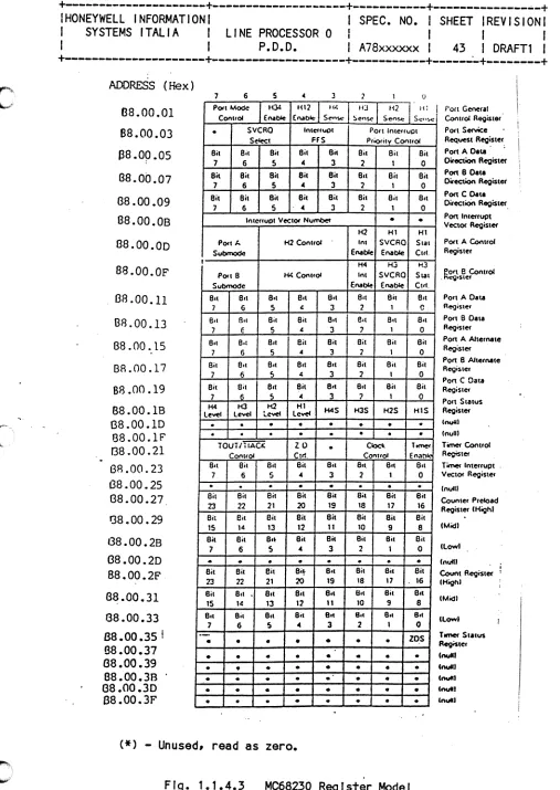
A reg i ster mode I that I nc I udes the correspond I ng Reg I ster Se I ects is shown In Fig. 1.1.4.3. For further Information refer to "16-BIT MICROPROCESSOR DATA MANUAL - 1983 MOTOROLA" page 4-509 - 4-537.
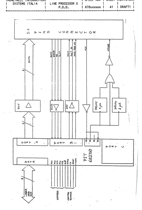
b) PARALLEL PRINTER INTERFACE - The Parallel Printer Interface allows the connect i on to pr inters wIth e I ectr I c para I I e I I nterface both of the IBM and CENTRONICS types. Fig. 1.1.4.1 shows the major block dIagram.
This interface Is Implemented by mean a programmable paral lei
Interface (MC68230) p I us some DR I VERs and RECE I VERs of the Low Power Schottky type. The dialogue wIth the prInter must be performed programming the MC68230 In the fol lowing mode:
- Port A must be set with Mode 0 and submode 01;
- Port B must be set with Mode 0 and submode lX;
- a I I pins of the Port A must be programmed
r
n output mode to drIve the printer data;("
(
IHONEYWELL INFORMATIONI I SPEC. NO. SHEET IREVISIONI
I SYSTEMS ITALIA I LINE PROCESSOR 0 I
I I I
I I P.D.D. I A78xxxxxx 39 I DRAFTl I
+---+---+---+---~+---+
PI/T PORT B (bit lnput/Qutput)
MSB LSB
7 6 5 4 3 2 0
I
X 0 I 0 0 I
I I I
I I I
I I I --- BUSY:
I I I
o
-->
ActiveI I I 1
-->
No Active1 I 1
1 1 1
---
ERROR1 I I
o
-->
No ActiveI I I 1
-->
ActiveI I I
1 1 1
---
PE (Paper Empty)I I I
o
-->
ActiveI I I 1
-->
No ActiveI I I
1 1
---
SLCT1 1
o
-->
ActiveI I 1
-->
No ActiveI 1
I 1
--->
INIT1 I
o
-->
No Active1 I t
-->
Active1 I
I
--->
SLCT INI
o
-->
No Active! 1
-->
Active1
--->
AUTO FEED XTo
-->
No Active 1-->
Active- handshake pin H4 must be used as an edge-sensitive status input pin to produce an interrupt to MC68000 when there is the trailing edge of the ACKNLG signal with the meaning of character request. The character shou I d be sent on I y if the pr r nter is ready (not busy) and no error conditIon is present.
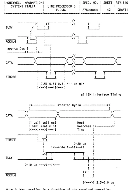
N.B. - The write of the data register (Port A) Involve a hardware generation of the data STROBE signal timing without software management necessity (see Fig. 1.1.4.2 which shows the timings relevant to CENTRONICS and IBM interfaces).
+---+---+----~---+---~---+
'HONEYWELL INFORMATION'
, SYSTEMS ITALIA 'LINE PROCESSOR 0
, P.D.D.
, SPEC. NO. , SHEET IREVISION'
, I , I
, A78xxxxxx' 40 'DRAFTl ,
+---+---+---+---~+---+
A register model that Includes the corresponding Register Selects Is shown In Fig. 1.1.4.3. For further Information refer to "16-BIT MICROPROCESSOR DATA MANUAL - 1983 MOTOROLA" page 4-509 - 4-537.
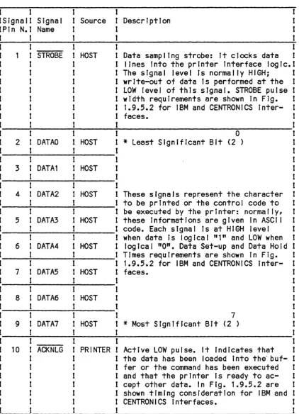
The I/O signa I s are made ava II ab I e v I a a CANNON connector hav I ng 37 paths with female pins: the connector pin out and a detailed
description of the Interface signals are shown In table 1.1.4.1.
The LPO board connects the printer unit via a signal cable (with
twisted-pair and shield) 5 meters max In lenght with a 37 pin
connector at the board unit end, and a 36 pin connector on the printer end.
The bits of the Port C are used In this way:
PIIT PORT C . (bit lnput/Qutput)
MSB LSB
7 6 5 4 3 2 0 ! !
o
O! 0 ! 0 0 0! ! ! ! ! ! ! ! ! ! ! ! t t t ! ! I I ! ! ! ! ! ! t ! t t t
INTERRUPT TO MASTER
o
--> Active1 --> No Active
INTERRUPT TO SLAVE
o
--> Active1 --> No ActIve
MASTER PROC. HALT STATE
o
--> No Active 1 --> Active ! ! ! ! ! ! ! I ! ! ! ! I ! ! ! ! ! ! ! ! ! ! ! ! I ! ! ! ! ! ! ! ! ! ! ! ! ! ! ! ! ! ! ! ! t ! ! !! --- TIMER INTERRUPT
t !
t
o
--> Active1 --> No Active
t-- ---> DIAGNOSTIC INV. CHECK
1--->
1--->
o
--> . . Active1 -->~Mct I ve
PRINTER INTERRUPT
o
--> Active 1 --> No ActivePRINTER INT. ACK.
o
c
IHONEYWEll INFORMATIONI SPEC. NO. I SHEET IREVISIONI I SYSTEMS ITAllA I liNE PROCESSOR 0 I I I
I I P.D.D. A78xxxxxx I 41 I DRAFT 1 I
+---+---+---+---+---+
...---- - - . i
IJOZZ:WIJI-O~
I'-__
f-_O_~_i-_-_-«
_ _ .-lr
'---_~_o_O::_I-_.
_f'1_-._-
---I·II~ -~
l--~
... N
p..~
I
,---"...
. "'"
....
:0: : :(
FIg. 1.1.4.1 Parallel PrInter Interface Block DJagram
i
v-i
i
[image:41.617.67.559.10.735.2]+---+---+---+---~---+ IHONEYWELL INFORMATIONI I SPEC. NO. I SHEET IREVISIONI
SYSTEMS I TALI A I LI NE PROCESSOR 0 I I I I I P.D.D. I A78xxxxxx I 42 I DRAFT1 I
+---+---+---+---~+---+
II
c
->1 ->1 III I I I BUSY
I I
1 I II
L
I I 11-1ACKNLG I I I
approx Sus I
--->1----1<--
II _ 1 1
-V I V II V V
DATA 1\ I
1\ II
1\
1\-I I I
I I
-I I I
II
I I _I I
II
STROBE I I I
I I
I 0.51 0.51 0.51 <-- us min 1<-->1<-->1<-->1
a) IBM .Interface Timing
1<--- Transfer Cycle --->1
_ I I _ _
V V V
DATA __ 1\ 1\ 1\ _ _
I !
11 usl1 usl1 usl Host·
I minI minI minI Response 1<--->1 1<-->1<-->1<-->1 Time I
1
_I 1
STROBE 1 1 1
1 0-20 us 1
1 1<--note 1-->1<-->1 1
1 I
->1 1_ 1
BUSY I ...::...-_;:..1 -;...1 --;.1 _ _ _ _ _ _ I I
0-10 us --->1--1<--- I 1
1 """"1 _ _ _ _ _ _
1<-- I
ACKNLG 1 I
1<--->1 2.5-6.6 us
Note 1: Max duration Is a function of the required operation.
b) CENTRONICS Interface Timing
[image:42.612.79.523.13.669.2]C
(')
o
+---+---+---+---+
IHONEYWELL INFORMATIONI I SYSTEMS ITALIA I
I I LINE PROCESSOR 0 P.D.D.
SPEC. NO. SHEET IREVISIONI
I I
A78xxxxxx 43 I DRAFT 1 I
+---+---+---+---~-+---+
ADDRESS (Hex)
7 6 5 3 ] u
--08.00.01 POll MOdel Control Enable I~ (nabf<, 1i12 S,," .... /1<: S,,"se I(l Sens., ti2 SC'I!J.e In
B8.00.03 • SVCRO InleffUOI Pon InleffuOI
Selecl FfS Priotilv Conuol
138.0p.Os 8.1 8.1 8'1 8i. 8i. 8i. 8.\ Bi.
7 6 5 c 3 2 I 0
88.00.07 8it Bi. 8i. 8il 8i. Bi. 8i. 8i.
7 6 5 c 3 2 I 0
88.00.09 8i. Bi. 8i. 8i. 8i. 8i. 8.\ 8 ••
7 6 5 c 3 2 I 0
88.00.08 InletruCII Vec.OI Numbet • •
H2 HI HI
88.00.00 POll'" H2 Conuol Inl SVCRQ Sial
Submode Enable Enable Clrl.
Ba.OO.OF
I HC H3
H3
PO<I 8 H< Conl'oI Inl SVCRQ Stal SubmOde Enable Enable CltI_
138.00.11 8.1 8i. 8 •• 8 •• 8 •• 8 •• 8 •• 8 •• 7 G 5 .c 3 2 1 0
BR.00.13 e.1 A •• 8i. 8it B.I e •• B.t B.t
7 € 5 4 3
,
1 088.00.15 B.t B.t 8 •• Bit Bit Bit Bit 8it
7 6 5 4 3 2 I 0
BR.OO.17 Bi. 8.t B.I Btt 8 •• 8 •• 8il Bit
7 6 5 4 3 2 t 0
88.00.19 Bit Bit B.I Bi. 8 •• Bil 8't 8't
7 6 5 4 3
,
I 088.00.18 H<I H3 H2 HI
H4S HlS H2S HIS
levet lewl :.~ le~
138.00.10
.
•·
• • • •·
BS.00.1F'
OS.00.21
. ·
·
•
·
• •·
TouT/HAC" ZO • CIOct Tomer
Conltol Cttt Cont.oI Ena~
OA.OO.23 B.t 8it 8i. 8 •• 8it 8'1. B'I 8.t
7 6 5
"
3 2 I 008.00.25
.
·
· ·
•·
· ·
138.00.27 8 •• 8't Bil 8i. 8.1 8it 8il B'I
23 22 21 20 19 18 17 16
I3S .00 .29 Bit Bit B'I 8il 8i. Bi. 8it Bit
15 14 13 12 11 10 9 8
138.00.28 8i. 8il Bt. 8it Bi. Bi. Bi. 8 ••
7 6 5
"
3 2 I 0OS.00.2D
·
·
· · ·
·
• •BS.00.2F 8 •• Bi. Bi. Bit 8.t Bit 8il Bi.
23 22 21 20 19 t8 17 16
88.00.31 8.1 8.t . Bt. Bi. 8.1 0.1 Bi. 8rt
IS 14 13 12 \I 10 9 8
8S.00.33 8.t 8il 8.1 8it 8rt 8.1 8.1 8.1
7 6 5 <I 3 2 I 0
88.00.35 I . • • •
•
•
• • lOSB8.00.37
88.00.39 •
•
•
•
• • • ••
• • • • • • •88.00.38 • • • • • • • •
8S.00.3D • • • • • • • •
88.00.3P • • • •
·
• • •(*) - Unused, read as zero.
Fig. 1.1.4.3 MC68230 Reg J ster Mode I
HONEYWELL CONF I DENT I AL AND PROPR lET ARY
I 1'011 General
Control R4I9isulC' POIt SeMce Request Register POll A 0.1.8. ; Direction Registef Pon 80.t. Oirection Regisler Pon C 0.1.8 Direclion Regislef Pon Inlertupt VectOt Register
Pon A Control Register
Port e Control . Fi"il,sIe.
POll A Oata Register Pon B Oata Register Port A Alternate Register Port B Alternate Regisle. Port C Oala Regisler POll StalUS Registet' lnultl (null! Timer Control Regisler Timer Interrupt . VectOf R4I9istet' Inultl
Counter Preload Register (High!
(MidI
(lowl
[image:43.612.42.549.8.723.2](
+---+---+---+---+
IHONEYWELL INFORMATIONI I SPEC. NO. I SHEET IREVISIONI
I SYSTEMS I TAL I A I LI NE PROCESSOR 0 I I I I
I I P.D.D. I A78xxxxxx I 44 I DRAFT1 I
+---+---+---+---+---+
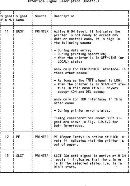
Table 1.1.4.1 Parallel-Printer Connector Pin Assignment and Interface Signal Description
I I I
ISignall Signal Source Description 1
! Pin N. 1 Name 1 1
1 1 1
1 1 1
1 STROBE HOST 1 Data sampling strobe: It clocks data I
1 I lines Into the pr Inter Interface log Ic.l
I I The signal level Is normally HIGH; I
I 1 write-out of data Is performed at the 1
1 1 LOW level of this signal. STROBE pulse 1
1 1 width requirements are shown In Fig. 1
1 1 1.9.5.2 for IBM and CENTRONICS Inter- 1
1 1 faces. 1
I----~---~---~I~---~---I
1 I 0 I
1 2 DATAO HOST 1
*
Least Significant Bit (2 ) 11 _ _ -..;... _ _ _
--=-____
1 11 1 1
1 3 DATA 1 HOST 1 1
1 1 1
1 1 1
4 DATA2 HOST 1 These signals represent the character 1
__
--=-___
--.,;:..-. ___
1 to be pr I nted or the contro I code to 11 be executed by the printer: normally, I
5 DATA3 HOST I these Informations are given In ASCI I 1
_ _ ~ _ _ _ --.,;:..-. _ _ _ I code. Each signal Is at HIGH level 1 1 when data Is logical "1" and LOW when 1 6 DATA4 HOST 1 logical "0". Data Set-up and Data Hold 1 1 Times requirements are shown In Fig. 1
--~---~----1 1.9.5.2 for IBM and CENTRONICS Inter- 1
7 DATA5 HOST 1 faces. 1
_ _ ~ ____ --.,;:..-. ____ l 1
1 I
8 DATA6 HOST I !
I !
--~---~----! 7 I
9 DATA7
10 ACKNLG
HOST I
*
Most Significant Bit (2 ) !I 1
1 1
PRINTER Active LOW pulse. It Indicates that !
1 the data has been loaded Into the' buf- I I fer or the command has been executed 1 1 and that the prInter Is ready to ac- I 1 cept other data. In Fig. 1.9.5.2 are 1 1 shown timing consideration for IBM and 1
[image:44.615.98.521.155.739.2]