DESIGN AND SIMULATION OF LOW POWER CONSUMPTION POLYMERIC BASED MMI THERMO-OPTIC SWITCH
NORIDAH MOHD RIDZUAN
A project report submitted in partial
fulfillment of the requirements for the award of the Degree of Master of Engineering (Electrical)
Faculty of Electrical & Electronic Engineering Universiti Tun Hussein Onn Malaysia
ABSTRACT
ABSTRAK
TABLE OF CONTENTS
CHAPTER TITLE PAGE
TITLE i
DECLARATION ii
DEDICATION iii
ACKNOWLEDGEMENTS iv
ABSTRACT v
ABSTRAK vi
TABLE OF CONTENTS vii
LIST OF TABLES x
LIST OF FIGURES xi
LIST OF ABBREVIATIONS xiii
LIST OF SYMBOLS xiv
LIST OF APPENDICES xvi
1 INTRODUCTION
1.1 Background of Project 1
1.2 Problem Statement 6
1.3 Objective of the Project 6
1.4 Scope of the Project 7
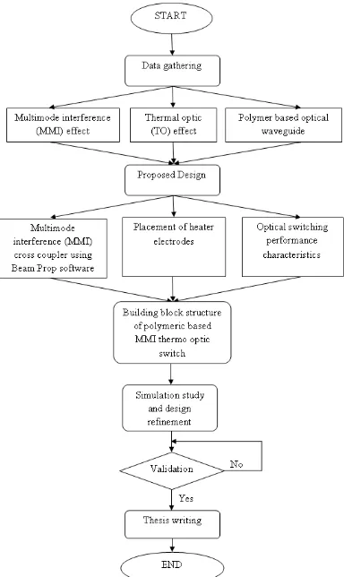
1.5 Project Methodology 7
2 OPTICAL WAVEGUIDE THEORY
2.1 Introduction 11
2.2 Basic configuration of optical waveguide 11 2.3 Planar Slab Optical Waveguide 13
2.4 Channel Optical Waveguide 15
2.5 Wave equation in optical waveguide 15
2.6 Effective Index Method (EIM) 18
2.7 Finite Difference Method (FDM) 19 2.8 Beam Propagation Method (BPM) 20 2.9 Previous works of MMI Thermo-optic switch 21
2.10 Conclusion 26
3 MULTIMODE INTERFERENCE THEORY AND THERMAL
ANALYSIS
3.1 Introduction 27
3.2 Multimode Waveguide 28
3.3 Self- imaging Principle 30
3.3.1 General Interference 33 3.3.2 Restricted Interference 34 3.3.2.1 Paired Interference 34 3.3.2.2 Symmetric Interference 35
3.4 Thermo-optic Effect 36
3.5 Heat Transfer 37
3.6 Induced Temperature Distribution 38 3.7 Induced Refractive Index Change 40
4 DESIGN AND SIMULATION OF POLYMERIC BASED MULTIMODE INTERFERENCE THERMO-OPTIC SWITCH
4.1 Introduction 42
4.2 Design of Single Mode Waveguide 43 4.3 Design of Multimode Interference Cross Coupler 44
4.4 Design of Heater Electrode 50
4.4.1 Heater Electrode 52
4.4.2 Heater Optimization 54
4.5 Conclusion 57
5 CONCLUSION AND FUTURE WORK
5.1 Conclusion 58
5.2 Recommendation for Future Works 59
REFERENCES 60
APPENDICES A-B 65
VITA 68
LIST OF TABLES
TABLE NO. TITLE PAGE
1.1 Summarization of published optical switch 4 4.1 Refractive indices of material used in the switch design 43
4.2 Optical power at Pout bar 46
4.3 Optical power at Pout cross 46
4.4 Measured crosstalk of optical switch 47 4.5 Thermal properties of material used in the proposed
MMI optical switch 51
LIST OF FIGURES
FIGURE NO. TITLE PAGE
1.1 Project methodology flow chart 9
2.1 Basic optical waveguide structure 12 2.2 Layers in planar slab optical waveguide 12 2.3 –x and –y view for the most common geometries for
channel waveguide (a) Buried channel waveguide (b) Strip-loaded waveguide (c) Ridge waveguide
(d) Rib waveguide 13
2.4 Planar slab optical waveguide structure and guiding layer (a) Symmetric dielectric waveguide
(b) Wave propagation in planar slab waveguide 13
2.5 Effective index method diagram 18
2.6 Schematic of the MMI optical switch 22 2.7 Schematic diagram of the MMI based optical switch 23 2.8 Schematic diagram of the MMI-MZI switch 25 3.1 Cross section view of multimode waveguide structure 29 3.2 (a) Slab optical waveguide
(b) Characteristic of step-index waveguide 30 3.3 Waveguide cross section with heat source 38 4.1 Cross section of the MMI based cross coupler 44
4.2 Layout of the MMI cross coupler 44
4.3 Configuration of the TO MMI switch 45 4.4 Crosstalk versus MMI cross coupler width for various
4.5 Design of MMI cross coupler in multi-pane mode 48 4.6 Layout 3D of the MMI cross coupler in BeamProp 48 4.7 The computed index profile at Z=0 49 4.8 The computed index profile at Z=700 49 4.9 BPM analysis for operation of MMI cross coupler 50 4.10 Configuration of the TO MMI switch with a straight
heating electrode. 52
4.11 Cross section of the TO MMI switch with a straight
heating electrode 53
4.12 Design of MMI cross coupler with heater electrode in
multi-pane mode 53 4.13 Temperature distribution plot for straight heater analysis
when power applied is 9.05mW. 54 4.14 Crosstalk versus the several strip width of straight
heater electrode 55 4.15 Driving power versus the several strip width of straight
heater electrode 56
1-A Division of the solution region into grid point for finite
difference calculation. 65
LIST OF ABBREVIATIONS
TEM - Transverse electromagnetic TE - Transverse electric
TM - Transverse magnetic MMI - Multimode interference
WDM - Wavelength division multiplexing MPA - Mode propagation analysis
TO - Thermo-optic
FDM - Finite difference method FEM - Finite element method DC - Directional coupler
MZI - Mach-Zehnder interferometer CT - Crosstalk
IL - Insertion loss ER - Extinction ratio
LIST OF SYMBOLS
SYMBOLS DESCRIPTION
R - Resistance
E - Electric field H - Magnetic field J - Current density ρ - Charge density
σ - Conductivity
D - Electric flux density B - Magnetic flux density
ε - Dielectric permittivity of the medium µ - Magnetic permeability of the medium n - Refractive index
λ - Wavelength
k - Wave number of a medium N - Effective index of the mode β - Wave propagation constant ω - Angular frequency
- Wave velocityv - Mode number
T - Waveguide thickness
Lπ - Beat length of the two lowest-order modes cv - Field excitation coefficient
E(y,z) - Field profile
WMMI - Multimode waveguide width
p - Periodic number of the imaging along the multimode waveguide
Q - Distributed thermal source per unit volume C - Specific heat
t - Time
k - Thermal conductivity
P - Supply power
w - Heater width
h - Heater length
I - Current through the heater electrode
dn/dT - Thermo-optic coefficient
LIST OF APPENDICES
APPENDIX TITLE PAGE
A Finite Difference Method (FDM) 61
CHAPTER 1
INTRODUCTION
1.1 Background of Project
As developments in optical fiber communications and integrated optical electronics scale up, the popularity for research work in this area increased as well.The enhancement in telecommunication system leads to the demand for increasing bandwidth capacity. Besides that, the world needs telecommunications system that can fit on the flexibility and re-configurability. Therefore, the implementation of optical communication system as a medium to transmit data signal has become major concern in telecommunication field due to its remarkable advantages on the performance.
Consequently, the field step forward onto the development of semiconductor optical devices which permitted very efficient and compact optoelectronic devices. These developments yield a rich variety of passive or active components such as optical splitters, optical coupler, variable optical attenuator, waveguide cross-couplers, optical switches and modulators.
In order to accomplish the current world demand, Wavelength Division Multiplexing (WDM) system which multiplexes multiple optical carrier signals on a single optical fiber by using different wavelength was introduced. In the WDM systems, signal routing and coupling devices such as optical switch are required to obtain large bandwidth.
Therefore, high speed and high capacity optical switch are crucially needed in current optical networks system. For this, it is necessary to research for good and tolerable performances of optical switch. Furthermore, it is important to develop optical devices that have low power consumption and crosstalk.
There are various optical switching technologies available today, such as Micro Electromechanical System (MEMs) (Dobbelaere et al., 2002, Leow et al., 2004), Electro optic switch (Lee et al.,2005, Wang et al., 2004 and Xiao et al., 2009), Thermo optic switch which originates from the temperature dependency of material‟s refractive index (Keil et al., 1996, Wu et al., 2006 and Al-Hetar et al., 2008) and Liquid Crystal Switch (Papadimitriou, 2003, Vazquez et al., 2003 and Shih et al., 2009). Thermo optic effects are one of the tuning effects that can change the refractive indices and modulate the propagation of light. Compared with electro optic effect, thermo optic effect is simpler and more flexible. Besides that, thermo optic effect can be found in all transparent materials (Nishihara et al., 1989)
al., 2005), Y-branch based switch (Yeo et al., 2006), multimode interference (MMI) based switch (Wang et al., 2006, Al-Hetar et al., 2008, Yin, 2008 and Jia et al., 2007) and combination of MMI-MZI based switch. Among these technologies, an MMI based switch has its own popularity due to their excellent performance and more than that, MMI structure is the most fabrication tolerance device. In addition, MMI devices owing to its advantages such as ultra-compact size, low loss and polarization insensitive (Soldano and Penning, 1995). In this work, MMI optical switch based on thermo-optic (TO) control is proposed due to itssimplicity and flexibility.
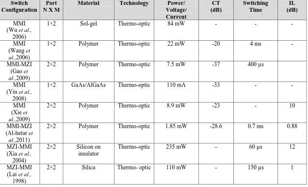
Table 1.1 Summarization of published optical switch
Switch Configuration
Port N X M
Material Technology Power/ Voltage/ Current CT (dB) Switching Time IL (dB) MMI (Wu et al.,
2006)
1×2 Sol-gel Thermo-optic 84 mW - - -
MMI (Wang et al.,2006)
1×2 Polymer Thermo-optic 22 mW -20 4 ms -
MMI-MZI (Gao et al.,2009)
2×2 Polymer Thermo-optic 7.5 mW -37 400 µs
MMI (Yin et al.,
2008)
1×2 GaAs/AlGaAs Thermo-optic 110 mA -33 - -
MMI (Xie et al.,2009)
2×2 Polymer Thermo-optic 8.9 mW -23 - 10
MMI-MZI (Al-hetar et al.,2011)
2×2 Polymer Thermo-optic 1.85 mW -28.6 0.7 ms 0.88
MZI-MMI (Xia et al.,
2004)
2×2 Silicon on insulator
Thermo-optic 235 mW - 60 µs 12
MZI-MMI (Lai et al.,
1998)
Switch Configuration
Port N X M
Material Technology Power/ Voltage/ Current CT (dB) Switching Time IL (dB) MMI (May-Arrioja
et al.,2006)
2×2 InGaAsp Electro-optic - -20 - -
Y-branch (Yeo et al.,
2006)
1×2 Hybrid polymer-silica
Thermo-optic 70 mW -35 - -
MZI-MMI (Liu et al.,2005)
2×2 Silicon on insulator
Thermo-optic 145 mW - 8 ± 1 µs -
MZI with 3 dB DC (Sohma et al.,
2002)
2×2 Silica Thermo-optic 45 mW - 3 ms -
MMI (Nagai et al.,
2002)
2×2 InGaAsP Electro-optic - -13 - -
Notes:
1.2 Problem statement
Optical switches are crucial components in optical networks. The ability to reconfigure optical switches with low power consumption has become a significant issue and is highly desirable. Furthermore switches with a small footprint are important for space, satellite and flight based applications. Therefore, the employment of Multimode Interference (MMI) thermo-optic switch in integrated optical circuit are required since they offer small size, robustness, good power balance, low polarization sensitivity, low insertion loss and ease of fabrication. In this project, the effect of single heater electrodes in terms of structure and placement will be analyzed to achieve low switching power consumption and crosstalk.
1.3 Objective of the project
This project aims to design a polymeric based thermal-optical switch using Multimode Interference (MMI) structure to achieve low switching power capability and reduce crosstalk figure. The optical switch will be designed on the 2x2 MMI cross coupler architecture of optical switch based on the general interference mechanism. The research objectives can be specified asfollows:
1. To design a 2×2 MMI cross coupler as basic architecture of optical switch. 2. To implement a polymer based thermo-optic (TO) effect in designing MMI
optical switch.
1.4 Scope of the project
In order to realize the research objectives which have been stated in previous sub section, the corresponding works to be carried out in this research have been identified as follows:
1. Design and optimization of MMI waveguide structure and dimension.
2. Design and optimization of heater electrode to the waveguide in terms of size and position to determine the optimum heater design for low switching power and crosstalk.
1.5 Project Methodology
This research begins with literature studies on MMI effect. The operation of optical MMI device is based on imaging effect principle. According to the self-imaging effect principle, an input field in a multimode waveguide is reproduced at periodic intervals along that waveguide. There are two types of interference mechanism, which are general interference and restricted interference. The restricted interference can be further divided into paired interference and symmetric interference. The optical switch in this project will be designed based on the general interference mechanism. Literature studies also included waveguide modeling techniques which are finite difference method (FDM), effective index method (EIM) and beam propagation method (BPM). These methods are adopted in solving the wave equation.
in order to obtain a cross coupler structure with high extinction ratio, low insertion loss and polarization-insensitive.
The following phase of the project will be on the studies of thermo-optic (TO) effect. This phase is required to understand the relationship of the parameters that governing the functionality of the device. Thus, heat distribution in the optical waveguides can be obtained and eventually, better placement of heater electrodes can be designed in order to ensure excellent performance of the optical switch.
1.6 Project outline
Chapter 1 presents an introduction of optical devices development in optical communication networking. The objective and the scope of this research study are presented as well.
Chapter 2 discusses the main principles of optical waveguide theory. The general wave equation which describes the propagation of light in the optical waveguide is derived using Maxwell‟s equation. The eigenvalue function for slab waveguide has been obtained using the ray-optics approach. The modeling techniques of channel waveguides have been discussed in detail, which include, the Effective Index Method, Finite Difference Method and Beam Propagation Method.
Chapter 3 explains the multimode interference (MMI) theory which is based on self-imaging principle. Classification on imaging mechanism into general interference and restricted interference has been explained in detail. The mathematical formulations that differentiate the properties of these interference mechanisms are briefly described. This chapter also covers the thermal analysis which is the fundamental aspect in designing the optimum heater structure. The temperature profiles of thermo-optic (TO) waveguides are analyzed by Finite Difference Method (FDM) and Finite Element Method (FEM).
Chapter 4 emphasizes on the simulation and optimization of the MMI TO switch. The optimization step starts from optimizing the MMI cross coupler. In order to design a TO switch and further analysis on heater‟s structure, the simulation was performed by employing BeamProp software from RSoft® due to its versatility.
CHAPTER 2
OPTICAL WAVEGUIDE THEORY
2.1 Introduction
This chapter presents the fundamental and the brief concepts of optical waveguide theory and techniques applied. The optical waveguide are definedusing the electromagnetic theory of light from Maxwell‟s equation while the techniques that have been employed for optical waveguide modeling are based on Effective Index Method (EIM), Finite Different Method (FDM) and Beam Propagation Method (BPM).
2.2 Basic configuration of optical waveguide
Figure 2.1 Basic optical waveguide structures (Koshibu, 1992)
Figure 2.1 shows the basic structure of optical waveguide, where the thin film has higher refractive index than either substrate or the upper cladding. Basically, there are two basic configurations of optical waveguide which are planar slab optical waveguide and channel optical waveguide.
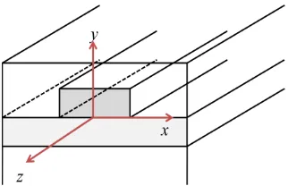
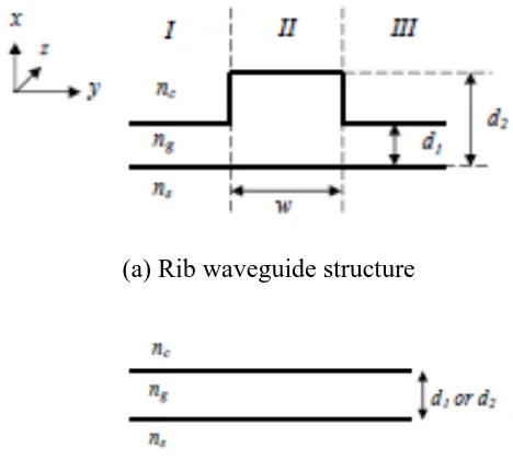
[image:25.612.139.520.432.571.2]Planar slab optical waveguide or 2-dimensional (2D) optical waveguide has optical confinement in only one transverse direction of thickness (-y direction) in the thin film. On the other hand, channel optical waveguide or 3-dimensional (3D) optical waveguide allow the light propagate in both direction (–x and –y direction).
Figure 2.2 Layers in planar slab optical waveguide(Koshibu, 1992)
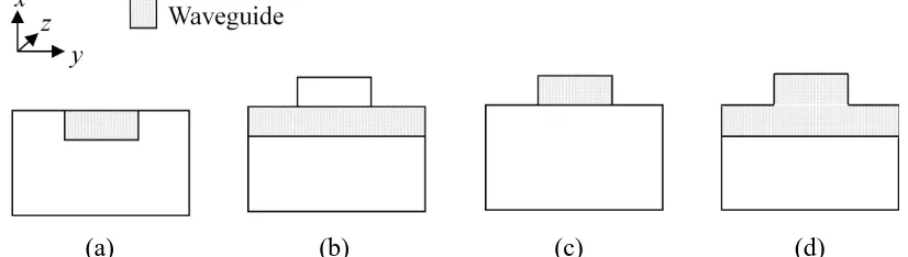
Figure 2.3 below shows –x and –y view for the most common geometries for channel optical waveguide. Channel optical waveguide structures are usually analyzed with the approximate technique namely; Effective Index Method (EIM) which will be described further in Section 2.4.
[image:26.612.123.536.186.303.2](a) (b) (c) (d) Figure 2.3 –x and –y view for the most common geometries for channel waveguide
(a) Buried channel waveguide (b) Strip-loaded waveguide (c) Ridge waveguide (d) Rib waveguide (Zappe, 1995).
2.3 Planar Slab Optical Waveguide
[image:26.612.119.541.464.566.2](a) (b)
Figure 2.4 Planar slab optical waveguide structure and guiding layer (a) Symmetric dielectric waveguide (b) Wave propagation in planar slab waveguide
(Reed G. T. and Knight A. P., 2004)
Figure 2.4(a) shows the planar slab optical waveguide structure where the waveguide layer (or core layer) has a refractive index ng, the lower cladding layer ns and
In order to obtain the mode propagation, the total internal reflection (TIR) is required and for this it needs any angle greater than critical angle, θc. For the two
borders, θc are;
θc(substrate) = (2.1 -a)
θc(upper) (2.1 -b)
Thus, the propagation can be described as the direction of wavenormal where the waves propagate along the z-direction with wavevector k where k = k0n1 as illustrated in Figure 2.4 (b). The wavevector k can be divide in y direction and z direction component particularly which gives;
(2.2 -a)
(2.2 -b)
As can be seen above, the wavevector in z direction indicate the rate at which the wave propagates. The wavevector kz is frequently replaced by the variable β. By defining the effective refractive index of the mode is N, thus gives;
(2.3)
Therefore the equation (2.2-a) becomes;
kz = β = Nk0 (2.4)
The guided modes that propagate along the z direction without „zig-zag‟ back and forth with refractive index, N make the corresponding range of N is
2.4 Channel Optical Waveguide
A channel waveguide or 3D confinement waveguide is the most practical structure for integrated optics. This type of structure allows the flexible routing of light around the waveguide surface (Zappe, 1995). Mathematical analysis has been performed in order to find the propagation constants and field profiles of all the modes in the waveguide. Nevertheless, it is complex matter to define the intended solution for channel waveguide compared with slab waveguide. Therefore, there are few methods that exist to simplify the calculations such as, Effective Index Method (Knox, 1970) and Method of Field Shadows (Zappe, 1995). The effective index method is simple and fast approach to determine the propagation constant and effective index channel (3D) waveguide (Zappe, 1995). The work conducted for this research, implementan effective index method.
2.5 Wave equation in optical waveguide
The optical waveguide are defined using wave equation which is origin from the Maxwell‟s equation. Maxwell‟s equations are set of four partial differential equations to show an electromagnetic wave. The following equations are simplified sets of Maxwell‟s equation (Sadiku, 2001);
D (2.6-a)
0
B (2.6-b)
t B E
(2.6-c)
where,
E = Electric field (V/m) H = Magnetic field (A/m) ρ = Charge density (C/m3) J = Current density (A/cm2)
Assuming that dielectric slab waveguide is formed from materials which are linear, isotropic and source free; the current density, J and charge density, ρ will equal to zero. In order to apply Maxwell‟s equation into wave equations analysis, it is necessary to specify the relations between D, E, H and B. The basic relation of electromagnetic theory for both electric and magnetic field states that;
H
B (2.7)
E
D
(2.8)where ε and μ are the permittivity and permeatibility of the waveguide medium. Both define as;
O R
(2.9)O R
(2.10)where,
O
= permeability of free spaceR
= relative permeability of mediumO
= permittivity of free spaceR
In order to derive the wave equation from Maxwell‟s equation, take the curl of equation (2.6-c) which then gives;
H
t
E
(2.11)
Equation (2.11) can be rewrite by plugging into equation (2.6-d) which will express the equation as follows;
22
t D t
J
E (2.12)
By applying the vector identity,
E
EE 2
(2.13)
to the left hand-side of equation 2.12, where , which gives;
2 2 t D t J
(2.14)
By assuming the moment of J = 0 and by substituting equation 2.8 into equation 2.14 yields the wave equation;
2 2 2 t E E
(2.15)
2.6 Effective Index Method (EIM)
Consider the channel (3D) waveguide with the rib type as shown in Figure 2.3(d). In effective index method, 3D optical waveguide is divided into region I, II and III as shown in Figure 2.5(a). Each region is then considered as 2D slab waveguide homogeneous in the y direction as shown in Figure 2.5(b). The effective index is then obtained by solving the eigenvalue function in x direction to produce Neff 1, Neff 2 and Neff 3 for region I, II and III, respectively. Using the obtained effective index, the system can be further modeled as new 2D slab waveguide homogeneous in x direction as shown in Figure 2.5(c). By solving the eigenvalue function in y direction, the final effective index, N can be obtained. The propagation constant, β can be calculated by using equation (2.4).
(a) Rib waveguide structure
(b) 2D slab waveguide homogeneous in the y direction
[image:31.612.205.439.350.560.2](c) 2D slab waveguide homogeneous in the x direction
2.7 Finite Difference Method (FDM)
Waveguide modeling can be divided into analytical and numerical technique. One of numerical technique is finite difference method (FDM). This method is popular due to its simplicity in the discretization procedure and the relative ease of implementation into a computer code. In the finite difference method, the governing equations are approximated by a point-wise discretization scheme where derivatives are replaced by deference equations that involve the value of the solution at the nodal point (Majumdar, 2005). Finite different method illustration can be seen in Figure 1-A (Appendix A). Finite difference equation can be derived by using several approaches, which include Taylor series method or control volume method. The three point finite difference formula for the second derivatives can be state as follows:
2 2
2 1, 2 , 1,
x j i E j i E j i E dx E d (2.16)
By adopting equation (2.16), the scalar wave equation (2.15) can now be written in basic discretized form as (Ibrahim, 2007)
2 2
0 2 2 2 2 , 1 2 1 , 1 , 1 , j i n k x y x j i E j i E j i E (2.17)
where i and j represent the mesh point corresponding to x and y direction respectively.
dxdy E dxdy E n k dy E d dx E d Ey y y y y 2 2 0 2 2 2 2 2 (2.18)Thus, the propagation constant of the mode and electric field distribution in the waveguide can then be solved using numerical method based on equation (2.18).
2.8 Beam Propagation Method (BPM)
The Beam Propagation Method (BPM) has been one of the most popular methods used in the modeling and simulation of electromagnetic wave propagation in dielectric waveguide. The advantages of BPM methods are (Baets et al., 1990);
(a) Optical field can be propagated over a large distance (thousands of wavelengths) with negligibly small errors,
(b) The computer code is simple and can be adapted to more complex simulation problem
Then considering the 3-D scalar wave equation;
(2.19)
The TE field will then separated into two parts; the axially slowly varying envelope term of Ф(x,y,z) and another one is the rapidly varying term of exp(- jkn0z). Thus E(x,y,z) can be expressed by,
By substituting equation (2.20) in equation (2.19) gives;
Ф Ф
Ф
where;
(2.21)
Assume the weakly guiding condition, we can approximate (n2 – n02) ≈2n0 (n - n0), in equation 2.21, that would result the equation to be as follows;
(2.22)
When n=n0, the first term will remain in right hand side of the above equation. Therefore, it is known that the first term of equation 2.22 represents free space propagation in the medium have refractive index of n0. While the second term of 2.22
represents the guiding function or influence of the region having refractive index n (x,y,z). Both side of equation 2.22 affect the light propagation simultaneously. In spite of this, for BPM analysis, the two terms are assumed can be separated and that each term affects the light propagation separately and alternately in the axially small distance in z -direction (Feit et al, 1978).
2.9 Previous works of MMI Thermo-optic switch
The fabricated thin-film small-area heater confirmed the simulation results with operating power consumption as low as 8.9 mW. The switching crosstalk obtained was less than -23 dB.
Figure 2.6 Schematic of the MMI optical switch (Xie et al., 2009)
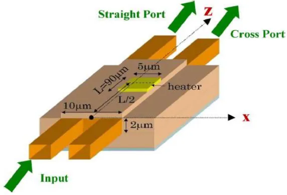
The polymer switch consists of thin polymer core/cladding layers, commercially available standard SU-8 epoxy/polymethyl-glutarimide (PMGI), coated on top of Si substrate with a thin-film heater placed above the device. The polymer refractive indexes are 1.575 and 1.480, respectively, at a wavelength of 1550 nm. A schematic structure of the MMI polymer switch is illustrated in Figure 2.6.
The polymeric materials used in the experiments are ZPU series from Zen Photonics, Inc. The refractive index of the polymers used for the core and cladding are 1.464 and 1.459, respectively. The size of the single-mode channel waveguide is 7x7m2. The width and length of the MMI region are 48 m and 3.6 mm, respectively. To realize the 250-m separation at the input–output ends of the device chip, bends are designed in the input–output access sections, as shown in Figure 2.7.
Figure 2.7 Schematic diagram of the MMI based optical switch (Wang et al., 2006)
The 2x2 MMI-MZI polymer thermo-optic switch in a high refractive index contrast (0.102) with a new structure design is realized by Al-hetar et al. (2011). A strongly guiding ridge waveguide with deep etching in the lower cladding has been used. In addition, ridge silicon is extended from the silicon substrate to the lower cladding and between heater electrodes. The main purpose behind this change in substrate layer is to localize the heating at a heated region and limit the heat diffusion elsewhere.
REFERENCES
Al-hetar A.M., Yulianti I., Supa‟at A.S.M., Mohammad A.B. (2008). Thermo-optic Multimode Interference Switch With Air And Silicon Trenches. Optics Communication, 281: 4653-4657.
Al-hetar A.M., Mohammad A.B., Supa‟at A.S.M., Shamsan Z.A., (2011). MMI-MZI Polymer Thermo-Optic Switch With a High Refractive Index Contrast. Journal of Lightwave Technology, Vol. 29, No. 2: 171-178
Besse P.A., Bachmann M., Melchior H., Soldano L. B., Smit M. K., (1994). Optical Bandwidth and Fabrication Tolerance of Multimode Interference Couplers. Journal of Lightwave Technology. Vol.12, No.6: 1004-1009.
Bryngdahl, O. (1973). Image Formation Using Self-Imaging Technique. Journal of the Optical Society of America. 63(4): 416-419.
Dai D., Yang L., Sheng Z., Yang B., and He S. (2009). Compact Microring Resonator With 2×2 Tapered Multimode Interference Couplers. Journal of Lightwave Technology. Vol. 27, No. 21:4878-4883.
Ibrahim M.H. (2007). Polymer Based Multimode Interference Optical Devices. Universiti Teknologi Malaysia: PhD Thesis.
Ibrahim M.H., Lee S-Y., Chin M-K., Kassim N.M., Mohammad A.B. (2007). Single Mode Optical Waveguide Based On Photodefinable Benzocyclobutene (BCB 4024-40) Polymer. Microwave and Optical Technology Letters. Vol. 49, No. 2: 479 - 481.
Inoue Y., Katoh K. and Kawachi M. (1992). Polarization Sensitivity of a Silica Waveguide Thermooptic Phase Shifter for Planar Lightwave Circuits. IEEE Photonics Technology Letters, Vol.4, No.1:36-38.
Keil N., Yao H.H., Zawadzki C., Lösch K., Satzke K., Wischmann W., Wirth J.V., Schneider J., Bauer J. and Bauer M. (2001). Hybrid Polymer/Silica Thermo-Optic Vertical Coupler Switch. Applied Physics B- Lasers and Optics. pp: 469-473.
Koshiba M. (1992). Optical Waveguide Analysis. McGraw-Hill, Inc.
Lei Gao, Jie Sun, Xiaoqiang Sun, Caiping Kang, Yunfei Yan and Daming Zhang (2009), Low switching power 2 x 2 thermo-optic switch using direct ultraviolet
photolithography process, Optics Communications 282: 4091–4094
Liu J., Yu J., Chen S., Xia J. (2005). Fabrication And Analysis Of 2 × 2 Thermo-Optic SOI Waveguide Switch With Low Power Consumption And Fast Response By Anisotropy Chemical Etching. Optics Communications 245: 137–144.
May-Arrioja D.A., Bickel N., and Likamwa P. (2006). Robust 2 × 2 Multimode Interference Optical Switch .Optical and Quatum Electronics. 38:557-566.
Nagai, S., Morishima, G., Inayoshi, H., and Utaka, K. (2002). Multimode Interference Photonic Switches (MIPS). IEEE Journal of Lightwave Technology. 20(4): 675-681.
Nishihara H., Haruna M., and Suhara T., (1989). Optical Integrated Circuits. New York: McGraw-Hill Book Co.
Okamoto K. (2006). Fundamental of Optical Waveguide, 2nd Edition, Elsevier Academic Press, United States of America.
Papadimitriou G. I., Papazoglou C. Pomportsis A.S. (2007). Optical switching. Wiley-Interscience.
Reed G. T. and Knight A. P. (2004). Silicon Photonics: An Introduction. John Wiley & Son, Ltd.
Sadiku M. N. O. (2006). Element of Electromagnetic, 3rd Edition, Oxford University Press, New York.
Schott AG Optical Glass Datasheet
SeongKu Kim, DongHo Cha, Qibing Pei and Kevin Geary (2010), Polymer Optical Waveguide Switch Using Thermo-Optic Total-Internal-Reflection and Strain-Effect, IEEE Photonics Technology Letters, Vol. 22, No. 4: 197-199.
Soldano L. B., Veerman F. B., Smit M. K., Verbeek B. H., Dubost A. H., and Erik C. M. Pennings E. C. M. (1992). Planar Monomode Optical Couplers Based on Multimode Interference Effects. Journal of Lightwave Technology. Vol. 10, No. 12: 1843-1850.
Soldano L.B. and Penning M.C. (1995). Optical Multi-Mode Interference Devices Based On Self-Imaging: Principle and Application. Journal of Lightwave Technology. Vol. 13.no 4: 615-627.
Supa‟at A.S.M., Mohammad A. B. and Kassim N.M. (2004). Polymer Based Directional Coupler Thermooptic Optical Switch. Jurnal Teknologi : 1-8.
Tocci C. and Caulfield H.J. (1994). Optical Interconnection: Foundation and Application. Artech House Publisher. Boston. London.
Ulaby. F.T. (1999). Fundamentals of Applied Electromagnetic. Prentice Hall, 1999 Edition.
Ulrich, R., and Ankele, G. (1975). Self-imaging in Homogeneous Planar Optical Waveguides. Applied Physics Letters. 27(6): 337-339.
Wang F., Yang J., Limei Chen L., Jiang X., and Wang M. (2006). Optical Switch Based on Multimode Interference Coupler. IEEE Photonics Technology Letters. Vol. 18, No. 2:421-423.
Xia J., Yu J., Wang Z., Fan Z. Chen S. (2004). Low Power 2 × 2 Thermo-Optic SOI Waveguide Switch Fabricated By Anisotropy Chemical Etching. Optic Communication 232: 223-228.
Xiao G.Z., Zhang Z., Grover C.P. (2004). A Variable Attenuator Based On a Straight Polymer-Silica Hybrid Channel Waveguide. IEEE Photonics Technology Letter. 16(11):2511-2513.
Xie N., Hashimoto T., and Utaka K. (2009). Very Low Power Operation of Compact MMI Polymer Thermooptic Switch. IEEE Photonics Technology Letters, Vol. 21, No. 18: 1335-1337.
Yaacob M. (2010). Benzocyclobutene Polymer in Glass Multimode Interference Thermo-optic Switch. Universiti Teknologi Malaysia: Master Thesis.
Yeo D-M., Shin S-Y, (2006). Polymer-Silica Hybrid 1 × 2 Thermooptic Switch With Low Crosstalk. Optics Communications. 267: 388–393.
Yin R., Teng J., Chua S. (2008). A 1 × 2 Optical Switch Using One Multimode Region. Optics Communication 281: 4616-4618.