International Journal of Emerging Technology and Advanced Engineering
Website: www.ijetae.com (ISSN 2250-2459, Volume 2, Issue 11, November 2012)70
Analysis, Modeling and Simulation of a Low Phase Noise
Frequency Synthesizer for High Sensitivity FM Receiver
Marianne M. Kamal
Renewable Energy Department Arab Organization for Industrialization
Abstract — This paper shows the design methodology of a low phase noise frequency synthesizer used for high sensitivity FM receivers. Stability and noise analysis for the frequency synthesizer are discussed in details with the effect of the critical parameters in each case. System modeling and simulation using Matlab was performed after determining the parameters of each block of the complete frequency synthesizer and simulation results are shown at the end of this work.
Keywords-component — Frequency synthesizer; System analysis; Noise analysis; matlab modeling.
I. INTRODUCTION
A frequency synthesizer is a system that generates different output frequencies from a given input reference frequency. The majority of frequency synthesizers utilize a classic PLL with a loop divider in the feedback path. This system produces an output frequency equal to the input reference frequency times the division factor, N. The division factor or modulus can be changed to synthesize different frequencies. The technique used to vary the modulus differs with the type of frequency synthesizer architecture that is used [1].
The output from frequency synthesizer can either be directly or indirectly related to the input. The direct synthesizer produces an output that is directly proportional to the input and is best known for its fast switching and very fine frequency resolution. It can also easily be integrated because no off chip components are required. But due to technology limitations, it takes large power consumption to synthesize very high frequencies directly. Usually a second frequency translation is needed to shift the center frequency to the GHz range.
[image:1.612.324.575.226.305.2]Fig. 1 shows the block diagram of the direct digital frequency synthesizer.
Fig. 1. Block diagram of direct digital frequency synthesizer
Indirect synthesizers operate by “locking” the output of a frequency source usually a VCO to that of another “cleaner” source known as the reference frequency. A phase-locked-loop-based frequency synthesizer with narrow loop bandwidth is the most commonly used technique due to its high performance, namely, low phase noise and low spurious tones. In addition, the narrow loop bandwidth makes it unsuitable in an agile system where fast frequency switching is needed. Fig. 2 shows the block diagram of the PLL based frequency synthesizer.
Fig. 2. PLL based frequency synthesizer
Another known architecture is the frequency
[image:1.612.326.577.451.541.2]International Journal of Emerging Technology and Advanced Engineering
Website: www.ijetae.com (ISSN 2250-2459, Volume 2, Issue 11, November 2012)71
[image:2.612.50.300.167.284.2]A block diagram of a PLL frequency synthesizer with a prescaler is shown in Fig. 3.
Fig. 3. Block diagram of frequency synthesizer with prescaler
This system produces an output frequency related to the input reference frequency, as in
ƒout = V * N * fref (1)
[image:2.612.329.571.298.440.2]In some cases another divider is added at the input
stage, before the phase detector block. The function of
this block is to divide the frequency of the crystal
oscillator by some divisor; R. the output from this
block is the comparison or reference frequency, which
is compared with the output from the programmable
divider in the phase detector block. This topology is
used in this paper and is shown in fig. 4.
Fig. 4. Frequency synthesizer with divider at the input stage
This paper is organized as follows; the second section discusses frequency synthesizers and their role in receivers. Section 3 states the key parameters in the synthesizer performance. Section 4 recapitulates the architecture and system specifications. In section 5 design methodology and system analysis, incorporating both stability and noise analysis, are presented. Matlab model and simulation results are presented in section 6. Finally, the conclusion is discussed in section 9.
II. FREQUENCY SYNTHESIZERS AND THEIR ROLE IN
RECEIVERS
Frequency synthesizer is an integral block in high performance wireless transceivers.
The role of frequency synthesizers in receivers is to generate an accurate signal used for frequency translation and channel selection.
[image:2.612.49.291.457.552.2]The choice of receiver architecture has a great influence on high easy it would be to implement a monolithic frequency synthesizer. As shown in fig. 5 an ideal frequency synthesizer generates a single frequency tone. In RF receiver case, it mixes with the received RF signal spectrum and shifts it down to base-band.
Fig. 5. Role of frequency synthesizers in receivers
The down- conversion of the modulated RF signal, needs a stable VCO to generate the LO signal, for channel selection. Frequency synthesizer is a sort of programmable VCO that generates various LO signals, from a common reference oscillator (usually a crystal oscillator) as shown in fig.6.
[image:2.612.323.578.542.671.2]International Journal of Emerging Technology and Advanced Engineering
Website: www.ijetae.com (ISSN 2250-2459, Volume 2, Issue 11, November 2012)72
III. KEY PARAMETERS IN FREQUENCY SYNTHESIZER’S
PERFORMANCE
The ideal output spectrum of a frequency synthesizer should be a single tone at the desired frequency in order to provide the reference frequency for frequency translation. All known VCO's have built-in phase noise spectrum, which makes the LO energy to spread over the nearby channels and this limits the signal to noise ratio (SNR) of the transceiver.
On the other hand, frequency synthesizer is an analog/mixed signal (AMS) device, in which the analog (VCO) circuit performance is greatly affected by the noise produced by the digital (divider and PFD) circuits. Hence, the key parameters in designing frequency synthesizers is to generate low phase noise and low-spur signals, while achieving fast settling time when it is hopping from a certain frequency to another. The settling time is largely determined by the loop bandwidth.
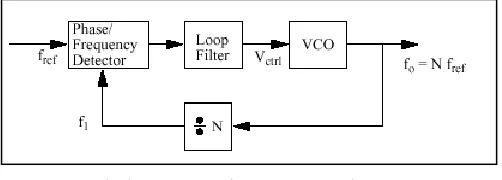
IV. ARCITECTURE AND SYSTEM SPECIFICATIONS
A. Architecture
Fig. 7 depicts the general block diagram of the architecture used in this paper, phase locked loop based frequency synthesizer with charge pump. This architecture is a digital PLL that uses a charge pump as the output of the PFD.
[image:3.612.53.291.544.657.2]The PFD compares the input reference signal and the feedback signal to produce two control signals up and down. These control signals control how much error current flows into the loop filter. The current of charge pump charges and discharges the loop filter to produce the VCO control voltage. The VCO signal is then divided in frequency via feedback divider and fed back to the phase/frequency detector.
Fig.7. Frequency synthesizer architecture
This architecture has the following advantages: (1) The phase frequency detector allows the synthesizer to have a pull in range that is only limited by the VCO tuning range.
(2) The static phase error is zero between the input reference signal and the feedback signal even if the reference signal is not equal to the center frequency of the VCO. (3) The architecture also exhibits high immunity to power supply variations.
B. System specifications
The frequency synthesizer has to generate signals with frequencies from 81.7 MHz to 91.7 MHz with steps of 25 kHz.
1) Reference Division Ratio
A crystal of 1MHz was used with the frequency synthesizer. Since the reference frequency is 25 kHz a "reference divider" was placed after the crystal oscillator. The divider ratio equals 1 MHz / 25 kHz = 40.
2) Loop Bandwidth
The design of the loop bandwidth involves
compromising between stability and noise performance. The loop bandwidth should be less than 1/10 of the reference frequency; therefore it should be less than 2.5 kHz.
3) Switching Time
In the switching time, the following rule is used: Switching time = 50 / fref (2)
Where fref is the reference frequency. Hence switching
time is equal to 2ms.
4) Feedback Division Ratio
The feedback divider consists of two-stage dual modulus divider (DMD). The divide ratios of the utilized feedback dividers are Nmin= 3268 and Nmax= 3668.
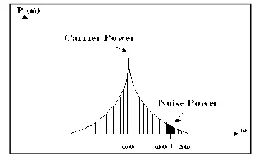
5) Phase Noise
It is well known that the frequency spectrum of an
oscillator with jitter consists of impulses with side
skirts of energy as shown in fig.8. These skirts are
known as phase noise.
[image:3.612.353.533.590.699.2]
International Journal of Emerging Technology and Advanced Engineering
Website: www.ijetae.com (ISSN 2250-2459, Volume 2, Issue 11, November 2012)73
The phase noise corrupts both the unconverted and down-converted signals. When the desired signal and a nearby interferer are mixed with non-ideal LO signal, the tail of the interferer spectrum corrupts the down-converted signal in the band of interest and thus reduces the signal to noise ratio (SNR). The degradation in the SNR of the system and reciprocal mixing effect are discussed in details in the system analysis section.
The synthesizer can be designed in such a way to minimize the phase noise of the output signal. Generally, the dominant sources of phase noise are from a noisy reference signal or from a noisy oscillator. Also other PLL non-idealities, such as phase-detector dead zone and power supply fluctuations can contribute to phase noise. The way the frequency synthesizer is designed depends on what is the dominant source of noise in the loop. The phase noise was chosen to be -70 dBc /Hz at least. This value was chosen according to the calculations performed in the system analysis as will be discussed later.
6) Spurious Frequencies
Typical systems require that all sidebands be about 60 to 70 dB below the carrier.
V. DESIGN METHODOLOGY AND SYSTEM ANALYSIS
In the following section the adopted design methodology that significantly enhances the performance of the frequency synthesizer is described in steps. Also system analysis which incorporates stability analysis and noise analysis for the system is described in this section.
A)Design Methodology
The design methodology can be summarized in the following steps [5]:
1) Determine VCO Tuning Range.
The maximum and minimum output frequencies of the VCO determine the tuning range of the frequency synthesizer. As previously mentioned the maximum and minimum frequencies are 81.7 MHz and 91.7 MHz respectively so the tuning range is determined as 10MHz.
2) Determine the loop division ratio
The loop division ratio range is the range that the programmable divider in the feedback path is operating. This is largely determined by the synthesizer frequency resolution Δƒ. Here, we choose Δƒ equal to the channel spacing 25kHz.
Therefore the division ratios (Nmin, Nmax) are determined from the following formula: Nmin = fmin/Δƒ, Nmax= fmax/Δƒ, where fmin and fmax are the minimum and maximum values of the VCO output frequency, respectively. So, we have: Nmin= 81.7 MHz/ 25KHz = 3268 and Nmax= 91.7 MHz/25KHz = 3668. The geometric mean Nmean= (NminNmax)= 3462 was used in
defining other synthesizer parameters.
3) Determine the Damping Factor
The "damping factor (ζ)," has an effect on the speed and stability of the system. As a compromise between speed and stability, ζ is optimally set to the value of 0.707.
4) Determine Natural Frequency
The "natural frequency (ωn)," has a significant effect on
the loop bandwidth. For a CPPLL with a passive loop filter, the "loop bandwidth (ω3dB)", is related to the natural
frequency by the following equation:
))
1
)
1
2
((
1
2
(
2 2 23
db n(3) So, when η = 0.707 is assumed we'll have: ω3dB = 2.06
ωn. It is desirable to make the loop bandwidth less than
1/10 of the input reference frequency (25 kHz) in order to avoid the continuous time approximations of the charge pump synthesizer breaking down. However, it is desirable to make the loop bandwidth as wide as possible in order to suppress the VCO phase noise that is the dominant source of phase noise.
In order to compromise between stability and noise performance, the loop bandwidth is set to: ω3dB = (ωref
/10)* 0.75 = 11.781 krad/s. This results in a natural frequency equal to: ωn = ω3dB /2.06 = 5.7 krad/s.
5) Determine VCO Gain.
The charge pump will no longer behave ideally if the VCO control voltage rises too high or falls too low. Therefore, the VCO control voltage is limited to VDsat from
the supply rails. With a power supply of 3.3V, a VCO control range of 2.2V can be assumed with a sufficient margin for process variations. This results in the following VCO gain: Kvco= 2π (81.7 - 91.7MHz) / 2.2= 28.6 Mrad/sV.
6) Determine Charge Pump Current and Loop Filter
Capacitor.
International Journal of Emerging Technology and Advanced Engineering
Website: www.ijetae.com (ISSN 2250-2459, Volume 2, Issue 11, November 2012)74
[image:5.612.81.254.136.291.2]C1=(I. Kvco) / (2π.Nmean.ωn2) (4)
Fig. 9. The Loop Filter
It is desirable to have a high charge pump current because it results in a higher loop gain and thus a more stable system. However, having a large charge pump current will result in a large capacitor. We choose I = 25 µA and C1 = 1.14 nF.
7) Determine Loop Filter Components.
The loop filter resistor is used to set the "damping factor (ζ)," according to the following equation: R= 2ζ/ωn. C1.
With ζ= 0.707,
ω
n= 5.7 krad/s, C1= 1.1nF, R= 225K. Thesecond loop filter capacitor, C2, used to suppress ripple in the control voltage is fixed to be less than a tenth of the main loop filter capacitor C1 so that the loop can still be considered a second order system. As C2 < C1/10= 0.11nF, so a value of 100 pF was chosen for C2.
B)System Analysis
The system analysis helps us to determine the impairment of the synthesizer on the whole receiver performance and determining the specifications of each block of the frequency synthesizer. Stability analysis and noise analysis are described in the following section.
1)Stability Analysis
There are certain conditions that must be satisfied for the frequency synthesizer to be a stable system. Care must be taken in choosing the type of loop filter that is used in the synthesizer and also in designing the bandwidth of the loop. Steady-state stability is an important criterion in the design. There are two ways to make the loop filter unstable: The first is to design a loop filter with a loop bandwidth that is more than 1/3rd of the comparison frequency. The second is to design a loop filter such that the poles of the closed loop system fall in the right hand plane.
In this work since the loop bandwidth was designed to be less than or equal 1/10 the comparison frequency as previously discussed, the first point of stability is achieved. The second point can be determined by examining the transfer function of the frequency synthesizer in an open state. From the general block diagram of the frequency synthesizer the transfer function, as in
(5)
[image:5.612.324.564.265.396.2]In fig. 10. it can be shown the transfer function of the frequency synthesizer is:
Fig. 10. Frequency Synthesizer general block diagram
(6)
(6)
Where, T(s) is the closed loop transfer function, G(s) is the open loop transfer function and equals KpF(s)Ko/s, Kp is the transfer function of the PFD in volts/Hz, Ko/s is the transfer function of the VCO in Hz/volt and F(s) is the transfer function of the loop filter.
The synthesizer is unstable when 1 + G(s) = 0, Hence, the system is unstable at the frequency where the magnitude of the open loop transfer function is unity and the phase angle is –180 degrees. This condition must be avoided by the proper selection of the loop filter parameters. If only a capacitor is used as the loop filter, the following transfer function is obtained:
(7)
International Journal of Emerging Technology and Advanced Engineering
Website: www.ijetae.com (ISSN 2250-2459, Volume 2, Issue 11, November 2012)75
In order for the loop to be stable a zero must be added to the loop filter in order to move the loop’s poles from the imaginary axis into the left plane. This is typically done by adding a series resistor to the loop filter so the transfer function becomes as in
(8)
Here there is an s term in the denominator. This means that there is a non-zero damping factor. Now, any excitation to the system will result in a dampened oscillation with a natural frequency equal to the following:
(9)
The damping factor of the system is equal to:
(10)
A formal stability limit is given in the following inequality, as in
(11)
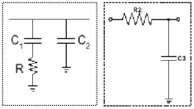
[image:6.612.332.549.194.403.2]The switching interaction between the charge pump and the loop filter causes a great deal of ripple on the VCO control voltage with the series RC loop filter. This ripple may be suppressed by adding a small capacitor, C2, in parallel with the loop filter. If C2 is made smaller then 0.1 C1 it may be neglected in the loop analysis because it is at a frequency greater then a decade from the zero of the filter. An extra pole is added to assist the attenuation of the sidebands at multiples of the comparison frequency that may appear, fig. 11.
Fig. 11. Loop filter circuit
The following table, TABLE I., lists the main specifications and components’ values for the loop filter to maintain a stable system.
Table 1
LOOP FILTER SPECIFICATONS
Specifications
Loop bandwidth 1.87k Cut off frequency 100k
Damping factor (ζ) 0.707
Natural frequency (ωn) 5.7krad/s
Components’ Values
R 225kΩ
R2 100kΩ
C1 1.1nF
C2 100pF
C3 220pF
2)Noise Analysis
[image:6.612.326.570.507.633.2]The well-known noise sources are specifically crystal reference (TCXO) noise; phase detector noise; and VCO phase noise. A plot of the commonly analyzed noise sources described above at the synthesizer output is shown in fig.12. The most effective noise source is the phase noise, so in the next part the phase noise and its effect, also the limitations on SNR of the receiver are discussed.
Fig. 12. Noise sources in frequency synthesizer
i) Phase noise and its effect on receiver Performance
[image:6.612.78.267.578.684.2]International Journal of Emerging Technology and Advanced Engineering
Website: www.ijetae.com (ISSN 2250-2459, Volume 2, Issue 11, November 2012) [image:7.612.55.290.138.282.2]76
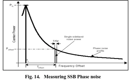
Fig. 13. Effect of phase noise tones in a receiverPhase noise is generally specified in dBc/Hz at a given offset frequency for a particular carrier. Therefore, the measure of phase noise is the difference between the absolute power level, Pfc, of the VCO at frequency fc and
the single sideband noise power, Poffset, at an offset frequency, foffset, in a specified bandwidth (usually 1Hz). This gives the equation for phase noise at any given offset, as in
(12)
With the units of the phase noise in dBc/1Hz (usually written as dBc/Hz) and P(fc) and P(foffset) in dBm and
dBm/Hz respectively. fig. 14. Shows SSB measure of phase noise.
Fig. 14. Measuring SSB Phase noise
ii) Phase Noise Limitations on Receiver Selectivity and Dynamic Range
Suppose that the ratio of the interferer signal power I to the desired signal power S is I/S. Let the interferer be displaced from the desired signal by a distance Δf, and let the receiver's IF bandwidth be BIF. The required phase noise performance to keep Sout = Nout ≥ (C/N) min, as in
Nop (Δf) / Posc ≤ 1 / ((I/S) (C / N) min BIF) (13)
Where, Nop (Δf) is the phase noise at offset Δf, Posc is the oscillator power, I is the Interfere signal power, S is the desired signal power, C/N is the carrier to noise ratio and BIF is the IF bandwidth.
Suppose that S/I = 1mA (0dBm) therefore I/S = 1000, C/N = 15.8 (12dB) and BIF = 10 KHz therefore, Nop (Δf) /Posc ≤ -82 dB. For Nop (Δf) / Posc = -70 dBc/Hz,
I/S = 63.3.
iii) Limit of Maximun Signal to Noise Ratio
The phase noise of a local oscillator will limit the maximum SNR that can be achieved by the receiver [4]. The following analysis shows the degradation that happens to the SNR of the system from the local oscillator phase noise. For a signal that has a 5-kHz RMS frequency deviation, the square of this signal is the modulating power contained in that signal, as in
Ps (5 kHz) = 25 MHz2 (14)
The power in the FM demodulator output is the square of the incidental frequency modulation, as in
PN = β
2f
(15)
Where βf is the Incidental frequency modulation, and can
be found, as in
(16)
This is a measure of the RMS frequency instability over a band of offset frequencies and £(f) is the phase noise, f2 is the frequency offset, fa and fb are the modulation bandwidth. The signal to noise ratio is the ratio between Ps and Pn is, as in
SNR = Ps / Pn (17)
If we take for example SNR of 12dB and signal bandwidth of 5 kHz, from (17) Pn= 6.2dB and from (15) ßf = 3.07dB. Phase noise £(f) can be calculated from (16) to be –56.3 dBc\Hz. This means that the local oscillator must not increase the value –56 dBc/Hz or else degradation in the total SNR will occur.
If £(f) changed to be –50 dBc/Hz, from the above equations SNR can be calculated equals to 5.78 dB. So SNR degrades from 12 dB to 5.78 dB due to a change in phase noise from –56.3 dBc/Hz to –50 dBc/Hz.
iv) Channel Blockers &Reciprocal Mixing
In wireless applications, out-of-band signals or blockers (Vb) can be much larger than in-band ones (Vd).
[image:7.612.64.279.474.608.2]International Journal of Emerging Technology and Advanced Engineering
Website: www.ijetae.com (ISSN 2250-2459, Volume 2, Issue 11, November 2012)77
In order to get rid of such nuisance, the SNR has to be increased by a headroom factor HR = (1+ (Vb/Vd) 2). In addition, when the desired signal and the interfere are mixed with non-ideal LO, the tail of interfering spectra corrupts the converted signal and thus reduces the SNR. This effect is called the reciprocal mixing [4]. The reciprocal mixing effect is shown in fig. 15.
The receiver noise floor in a one-Hertz bandwidth is the sum of the receiver's noise figure, F, in dB and -174 dBm/Hz,
Pn=F-174 (dBm/Hz) (18) The noise generated in the receiver from a nearby carrier is the sum of the carrier power; Pc, in dBm and the SSB phase noise of the local oscillator at an offset frequency equal to the difference between the carrier frequency and the frequency to which the receiver is tuned.
[image:8.612.326.567.143.246.2]Po = Pc + £(f) (dBm/Hz) (19)
Fig. 15. Reciprocal Mixing
The apparent noise floor of the receiver is the sum of these two powers. For Pc = -107 dBm, we have Pn = F - 174 = 12 - 174 = -162 dB and Po = -107 - 56.3 = -163.3 dBm/Hz. So, the apparent noise floor = -159 dB and phase noiseat this offset is equal to – 70 dBc/Hz.
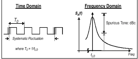
v)Spurious Tones
[image:8.612.57.291.322.475.2]The other critical performance parameter in a frequency synthesizer is the spurious tone level. Spurious tones can be defined as systematic timing fluctuations in an oscillator waveform. Spurious tones are measured in dBc at a specific frequency location in the spectrum. It is simply the power difference between the carrier and spurious tone signals in dB as shown in fig. 16. The effect of spurious tones in a radio transmitter and receiver is very similar to that of phase noise.
Fig. 16. Time and Frequency Representations of Spurious Tones
The most common type of spur is the reference spur. Depending on the cause of the reference spurs (either leakage or mismatch), the spurs may behave differently when the comparison frequency or loop filter is changed. Fig.17. shows the idea of the reference spur.
Fig. 17. Typical reference Spur plot
Reference spurs are intended to refer to spurs that appear at spacing equal to the comparison frequency from the carrier.
At lower comparison frequencies leakage effects dominates pulse effects, the later refers to inconsistencies in the pulse width of the charge pump.
VI. MATLABMODEL AND SIMULATION RESULTS
[image:8.612.341.547.335.504.2]International Journal of Emerging Technology and Advanced Engineering
Website: www.ijetae.com (ISSN 2250-2459, Volume 2, Issue 11, November 2012)78
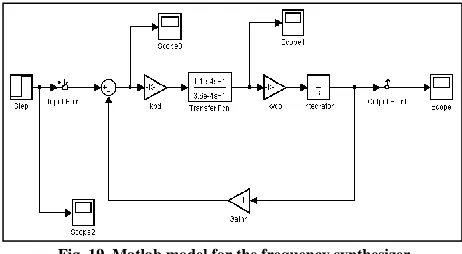
Fig. 18. Frequency Synthesizer linear model [image:9.612.53.279.140.240.2]Fig. 19. Shows the model developed in Matlab for the frequency synthesizer.
Fig. 19. Matlab model for the frequency synthesizer
[image:9.612.330.560.142.384.2]The open loop transfer function response is shown in fig. 20.
Fig. 20. Open loop response
The closed loop transfer function response is shown in fig. 21.
Fig. 21. Closed loop response
[image:9.612.51.282.287.414.2]Step response of the frequency synthesizer was simulated in Matlab and the output is shown in fig. 22.
Fig. 22. Step response
[image:9.612.337.546.423.629.2] [image:9.612.56.278.450.672.2]International Journal of Emerging Technology and Advanced Engineering
Website: www.ijetae.com (ISSN 2250-2459, Volume 2, Issue 11, November 2012) [image:10.612.58.268.124.505.2]79
Fig. 23. Root locusFig. 24. Impulse response for the system
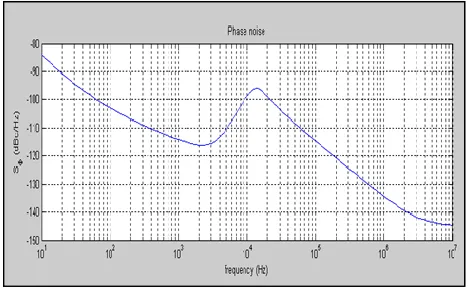
[image:10.612.324.564.224.373.2]Fig. 25. shows the phase noise of the frequency synthesizer as simulated in Matlab. The phase noise obtained from the simulation = -83 dBc/Hz.
Fig. 25. Phase noise simulation results
The noise contribution from both the loop filter and the phase frequency detector was also simulated and the results showed minimal noise added to the system from these two blocks. The noise from the loop filter was found to be -140 dBc/Hz, while that of the phase frequency detector is approximately -138 dBc/Hz. Fig. 26. shows the simulation results for the above mentioned blocks.
Fig. 26. Noise contribution from loop filter and phase frequency detector
VII. CONCLUSION
In this work design and system analysis of narrow band frequency synthesizer parameters using mathematical model and simulation using Matlab was discussed. The designer of the frequency synthesizer faces trade-offs related to the resolution, convergence speed, power and phase noise of the synthesizer. The basic factor that limits the performance of the narrow-band synthesizer is the low sampling rate of the phase difference. This sampling rate is dependent upon the frequency step of the synthesizer which is equal to the narrow loop bandwidth.
Charge pump frequency synthesizer with prescaler architecture was chosen in the paper as this topology is capable of operating at high VCO frequency with fast settling time. The results showed that the system has minimum spurs and low phase noise together with good settling time and stable loop.
REFERENCES
[1] F. Gardner, Phase Lock Techniques, Wiley, New York, second edition, 1967.
[2] B. Razavi, "Analysis, Modeling and Simulation of Phase Noise in Monolithic VCO Design," Proceedings of CICC, 1995.
[image:10.612.49.284.554.699.2]International Journal of Emerging Technology and Advanced Engineering
Website: www.ijetae.com (ISSN 2250-2459, Volume 2, Issue 11, November 2012)80
[4] C. John Grebenkemper, Local oscillator Phase noise and its effecton receiver performance, Tech. note, WJ communications, Inc. 1999.