International Journal of Emerging Technology and Advanced Engineering
Website: www.ijetae.com (ISSN 2250-2459, ISO 9001:2008 Certified Journal, Volume 7, Issue 10, October 2017)
267
Design of Efficient Cache Memory with Power Optimization
Akkala Subbarao
1, Pratik Ganguly
21
Associate Professor, 2Junior Research Fellow, ECE Department, SR Engineering College, Warangal, India
Abstract— In System on chip (SoC) development, performance improvement is an important issue. The data cache memory connected to SoC consumes lot of power. The cache architecture cannot be considered individually for a particular application and consequently large part of cache memory is not utilized. In this paper, an energy efficient cache memory is designed and is integrated to SoC. The effectiveness of the designed hardware-software controlled cache is verified after integration and the cache memory is also power optimized.
Keywords— Cache, Cache architecture, Energy efficiency performance improvement, SoC, Software controlled cache,
I. INTRODUCTION
Cache is generally used to increase the access to storage devices mainly in memory units, disk drives and tape. Applications can access storage of data within a particular time. Storage device is made by a technology, which has a fixed cost and access time. Storage device with faster technologies have more cost and lesser access time when compared to devices with slower technologies. The application accesses are generally done by the cache and generally the overall access time of cache is faster when compared to big storage devices.
The main problem existing with the normal hardware- oriented cache in system is that it may not have the expected data at any particular point of time, though their performance is good. If data is not present in cache, it becomes slow. A flexible procedure is always required which provide instructions and data to be pinned and should allow cache contents to change faster. A software controlled [1] cache provides a solution to this. In trhis paper, hardware–software controlled cache is designed for better performance.
A. Working Principle of Cache
A general cache [2] consists of tag and data. The tags consist of valid entries in cache memory, one each per data entry. Each tag identifies the contents of the corresponding data entry. Mostly, the hardware caches work in such a way that one indexes a cache and stored data is indicated by associative cache. When the tag match occurs, the data in data entry is read out. Cache lookup procedure can be divided into three methods mainly i.e. direct mapped, fully associative cache and set-associative cache.
In fully associative lookup, tag of each data existing in the cached is checked by a search. If a tag matches the tag of the required address, then it is called as a cache hit and the cache has requested data. In a direct mapped lookup method, a given data is available in cache entry, which is obtained by sequence of address bits of data. Directly mapped cache is extremely fast in search because there is only one location dedicated for any particular data. In directly mapped caches, a small portion of the key can be used for choosing a data set. In case of directly mapped caches, one cache line only is available at a specified index
II. ORGANIZATION OF CACHE ARCHITECTURE
Different cache organizations are present based upon the cache indexing and tag information details. The address of the physical or virtual data corresponds to the key of the database. Generally, the instruction and data caches are mapped directly.
A. Physically Indexed, Physically Tagged Architecture In this type of cache design, the virtual address must be converted before the cache is accessed since the cache should be indexed and tagged with related physical address location. Since the cache can be controlled fully by hardware in this case, the operating system is not responsible for cache management. Since address translation lies in the critical path, this is the disadvantage of the design. When clock speed increases, this becomes an issue. As the memory size increases, the larger Translation Lookaside Buffers (TLB) [3] are used to map bigger data sets.
International Journal of Emerging Technology and Advanced Engineering
Website: www.ijetae.com (ISSN 2250-2459, ISO 9001:2008 Certified Journal, Volume 7, Issue 10, October 2017)
268 Fig.1. Physically indexed, physically tagged architecture
III. ISSUES IN CACHE AND RESULTS
Hardware caches are quite energy inefficient since they have to constantly perform counter updates for tracking least frequently used data. In addition to energy inefficiency, a significant area of the cache is occupied by the decision-making logic making less area available for the storage. Moreover, since the data is not guaranteed to be found in the cache, the latency times encountered by the load stores in the presence of hardware caches are unpredictable. Thus, embedded processors rarely follow hardware cache organization.
On the other hand, caches implemented in software [4][5]only can be inefficient and can result in poor design since it must keep and update some information such as the access tags in software and every cache hit also goes for look-up and staleness check which can be very expensive in terms of latency, space and energy costs.
Due to these limitations of caches, hardware-software collaborative cache has been design in this research. Cache design is done by combining software and hardware features of cache memory. For multimillion gate sized SOC, performance improvement and power reduction are the most important factors. By combining software and hardware features of cache memory, these issues were dealt here.
Various SoC blocks such as Inter IC Sound (I2S), Inter Integrated Circuit (I2C) and Serial Programming Interface (SPI) are designed using VHDL language. Cache memory is designed using both VHDL and C-language and each block is simulated using Questa software of Mentor Graphics. The results are specified below, which meet expected results.
A. I2C
I²C is a multi-master and multi-slave single-ended communication protocol. It is mainly used for connecting slower speed peripherals to the microcontrollers and processors with in small distance range. I²C is also used in
intra-board communication. I²C has mainly two
bidirectional lines and they are Serial Data Line (SDA) and Serial Clock Line (SCL). These lines are pulled up by resistors. Typical voltages are +3.3 V or +5 V even though other voltages are also allowed.
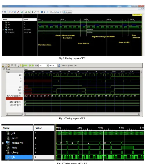
The design of I²C consists of 7 or 10-bit address. The regular bus speeds of I²C are 10 Kbit/s low-speed mode and 100 Kbit/s in standard mode. Even lower clock frequencies can also be allowed. I²C can run on faster speeds such as 400 kbit/s in Fast mode, and 3.4 Mbit/s in High Speed mode. I²C design has been completed using VHDL and its simulated result is specified in Fig. 2.
Data transfer will be started with a START bit when SDA is pulled low and SCL is high. 1st data bit level is set by SDA when SCL is low in time of blue bar. When SCL is high for the first bit, the data will be sampled. The same process is repeated by by changing SDA when SCL is low and when SCL is high. The data will be read.
A STOP bit occurs when SDA is high and SCL is also high. To avoid any false detection, SDA is translated on falling edge of the SCL. The SDA is then sampled and taken on rising edge of the SCL.
B. I2S
International Journal of Emerging Technology and Advanced Engineering
Website: www.ijetae.com (ISSN 2250-2459, ISO 9001:2008 Certified Journal, Volume 7, Issue 10, October 2017)
269
Fig. 2 Timing report of I2C
[image:3.612.57.558.138.704.2]Fig. 3 Timing report of I2S
International Journal of Emerging Technology and Advanced Engineering
Website: www.ijetae.com (ISSN 2250-2459, ISO 9001:2008 Certified Journal, Volume 7, Issue 10, October 2017)
270 The I²S bus can be used to separate clock and serial data signals, which can result in a lower jitter than than special communications systems that obtains the clock from a stream of the data.
I²S has 3 lines mainly Bit clock line and Word select line for Left & Right Channel selection. It has one multiplexed data line. The Design of I2S has been done using VHDL. The timing report of I²S is obtained from Questa as shown in Fig. 3.
Data can be transferred either with the least significant bit first or most significant bit first. The timing report in Fig. 3 shows that the Left channel was sent before the right channel for a particular signal.
C. UART
In this Universal Asynchronous Receiver and
Transmitter (UART), communication can be in one direction only ie. Simplex or bidirectional data transfer ie. Full duplex or Half duplex, in which devices turn from transmitting to receiving and vice versa. Design of UART was done with VHDL. The result of its simulation report of UART is mentioned in Fig. 4.
[image:4.612.51.287.479.686.2]UART takes data bytes and sends individual bits in sequential manner. At receiving end, a second UART assembles the bits back into bytes. Each UART has a shift register, which provides conversion between serial and parallel data. Generally, transmission of digital Serial bits or bytes in a single wire or medium provides less cost than parallel transmission.
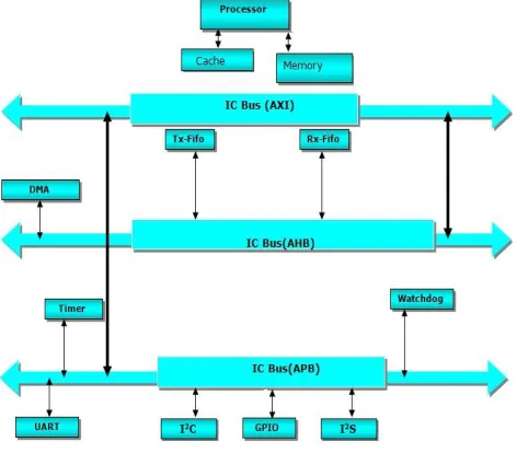
Fig. 5 SoC Design
The ARM based Advanced Microcontroller Bus Architecture (AMBA) is open-standard and on-chip interconnect specification. It is used as to connect and manage different blocks of SoC designs. It is used in the development of multi-processor designs having large numbers of controllers along with peripherals. Recently, AMBA bus-bridge became famous in the design of ASIC and SoC, in which peripherals exist with different speeds.
The AMBA is an open-standard, on-chip interconnect specification used as a connection and management of different blocks in SOC designs. It is used in the development of multi-processor designs having large numbers of controllers with peripherals. Now days, AMBA bus-bridge is widely used on a range of ASIC and SoC having peripherals of different speed. Top level integration of cache memory with SoC is shown in Fig. 5. The high speed Advanced eXtensible Interface (AXI) bus has been used with Advanced High Performance Bus (AHB) bus to support different speed peripherals in SoC such as I2C, I2S, GPIO, USB and UART as shown in Fig. 5.
[image:4.612.327.563.491.639.2]The complex integrated SoC shown in Fig. 5 has been designed with low power consumption by usage of power optimization script. Clock gating and Dynamic voltage scaling have been used as well to decrease the power consumption of SoC. Fig. 6 shows the result of execution time with respect to designed cache configuration. By usage of advanced power optimization software and optimized software controlled cache architecture, we have minimized the power consumption and increased the performance of SOC to a greater extent.
Fig. 6 Execution Time with cache configuration
International Journal of Emerging Technology and Advanced Engineering
Website: www.ijetae.com (ISSN 2250-2459, ISO 9001:2008 Certified Journal, Volume 7, Issue 10, October 2017)
271 Toggle coverage is 72% which is above our expectation level of 60%. As all the signals or pins should not toggle in both ways i.e. from 0-1 and 1-0 and toggling entirely depends on the requirement.
After efficient cache memory design and integration in SoC, performance of SoC has been improved to a greater extent with the applied techniques such as Clock gating, Dynamic voltage scaling by Power reduction software script and the final SoC efficiency improvement is around 18-19% when compared to standard SoC without efficient cache memory design.
IV. CONCLUSION
This paper focused on design of hardware-software oriented cache management by using SRAM cache on SoC. The SoC was designed with various blocks such as I²C, I²S, UART and Cache memory. The designed SoC was checked for efficiency and power reduction. The power reduction is obtained by implementing various techniques such as clock gating, dynamic voltage scaling by Power reduction software script and overall 18-19% efficiency is improved in comparison to standard SoC without advanced cache memory design.
Acknowledgements
The authors thank DST-SERB for providing financial support for this research work
REFERENCES
[1] Jacob, B. L. and Mudge, T. N. ―Software-managed address translation‖, In Proc. Third International Symposium on High Performance Computer Architecture (HPCA-3), San Antonio TX, pp. 156–167, February 1997.
[2] Jouppi, N. P. ―Cache write policies and performance‖, In Proc. 20th Annual International Symposium on Computer Architecture (ISCA-20), May 1993, pp. 191–201.
[3] Jacob, B. L. and Mudge, T. N. ―A look at several memory-management units, TLB-refill mechanisms, and page table organizations.‖ In Proc. Eighth Int’l Conf. on Architectural Support for Programming Languages and Operating Systems (ASPLOS- 8), San Jose CA, October 1998, pp. 295–306.
[4] Bathen, L. A. D. and Dutt, N. D. ―Software Controlled Memories for Scalable Many-Core Architectures‖, IEEE International Conference on Embedded and Real-Time Computing Systems and Applications, 2012, pp. 1-10.