A U G U S T 1 9 9 3
WRL
Technical Note TN-37
Boolean Matching for
Full-Custom ECL Gates
The Western Research Laboratory (WRL) is a computer systems research group that
was founded by Digital Equipment Corporation in 1982. Our focus is computer science
research relevant to the design and application of high performance scientific computers.
We test our ideas by designing, building, and using real systems. The systems we build
are research prototypes; they are not intended to become products.
There two other research laboratories located in Palo Alto, the Network Systems
Laboratory (NSL) and the Systems Research Center (SRC). Other Digital research groups
are located in Paris (PRL) and in Cambridge, Massachusetts (CRL).
Our research is directed towards mainstream high-performance computer systems. Our
prototypes are intended to foreshadow the future computing environments used by many
Digital customers. The long-term goal of WRL is to aid and accelerate the development
of high-performance uni- and multi-processors. The research projects within WRL will
address various aspects of high-performance computing.
We believe that significant advances in computer systems do not come from any single
technological advance. Technologies, both hardware and software, do not all advance at
the same pace. System design is the art of composing systems which use each level of
technology in an appropriate balance. A major advance in overall system performance
will require reexamination of all aspects of the system.
We do work in the design, fabrication and packaging of hardware; language processing
and scaling issues in system software design; and the exploration of new applications
areas that are opening up with the advent of higher performance systems. Researchers at
WRL cooperate closely and move freely among the various levels of system design. This
allows us to explore a wide range of tradeoffs to meet system goals.
We publish the results of our work in a variety of journals, conferences, research
reports, and technical notes. This document is a technical note. We use this form for
rapid distribution of technical material. Usually this represents research in progress.
Research reports are normally accounts of completed research and may include material
from earlier technical notes.
Research reports and technical notes may be ordered from us. You may mail your
order to:
Technical Report Distribution
DEC Western Research Laboratory, WRL-2
250 University Avenue
Palo Alto, California 94301 USA
Reports and notes may also be ordered by electronic mail. Use one of the following
addresses:
Digital E-net:
DECWRL::WRL-TECHREPORTS
Internet:
[email protected]
UUCP:
decwrl!wrl-techreports
Boolean Matching for Full-Custom ECL Gates
Robert N. Mayo
Herve Touati
Abstract
@AbstractForm{ TitleString="Boolean Matching for Full-Custom ECL
Gates", AuthorString="Robert N. Mayo, Herve Touati",
LabName="Western Research Laboratory", DocDate ="June 1993",
DocLabel="Technical Note TN-37", DocTag="TN-37", AbsBody={ We
present a technology mapper for full-custom ECL gates. These gates are
characterized by high fanins and a regular structure. Full-custom gates
dif-fer from ECL library gates in that a full range of structures is available as a
single form, rather than a large number of individual gates that sparsely
cover the possible design space.
This paper presents a complete boolean matching algorithm and gives a
proof of its correctness. We show that it can efficiently map logic into the
general ECL gate form. We also show two variants of the algorithm, and
show that they give poorer results with no savings in runtime.
The mapper described in the paper is a necessary component of a CAD
system for designing ECL microprocessors. Manual design of full-custom
ECL gates would not be acceptable for control logic since it is a tedious,
er-ror prone, and lengthy activity. Nor would a gate-array style mapper and
library with a limited number of gates be acceptable, because this makes less
effective use of the inherent speed of the technology. } }
Abstract
We present a technology mapper for full-custom ECL gates. These gates are characterized
by high fanins and a regular structure. Full-custom gates differ from ECL library gates in
that a full range of structures is available as a single form, rather than a large number of
individual gates that sparsely cover the possible design space.
This paper presents a complete boolean matching algorithm and gives a proof of its
correctness. We show that it can efficiently map logic into the general ECL gate form. We
also show two variants of the algorithm, and show that they give poorer results with no
savings in runtime.
1
Introduction
This paper presents a specialized form of boolean function mapping that is efficient for full-custom designs in the ECL (Emitter Coupled Logic) circuit family. By full-custom we mean the gates are not selected from a library, but are instead built as needed within the bounds of what the technology allows. This allows us to have many more gates than could be placed in a library. Existing libraries[7] contain only a portion of the possible gates, resulting in both wasted area and time.
Our current application is a full-custom 64 bit ECL BiCMOS microprocessor. The characteristics of ECL important to this application are: complex gates with wide fanins, free negation of gate outputs, low gate delays, low wiring delays (due to low logic swings and high currents), and a density comparable to CMOS for structures other than RAM. The combination of these factors allows implementation of fast microprocessors where power consumption is not important and where CMOS RAM may be implemented elsewhere on the same chip, as is the case in our application. The advantages of ECL have been demonstrated with an experimental 300Mhz 115W 32b full-custom ECL microprocessor called BIPS0. [4]
The technology mapper described in this paper takes advantage of two particular features of ECL: high fanin and a regular gate structure. The mapper is an essential part of the CAD system[6] we are using to design our next generation ECL microprocessor.
2
ECL Gates
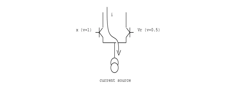
ECL is a current-steering technology. That is, a current source provides a fixed amount of current, which is then routed in one of two directions using differential pairs of transistors (Figure 1). The differential pair works by comparing the voltages on the bases (inputs) of the transistors, and routing the current through the transistor that has the highest base voltage. In addition to voltages corresponding to logic values 1 and 0, a voltage is available that corresponds to the logic value 0.5. This allows us to route current with only a single input, rather than requiring two inputs that are complements of each other. This voltage is called the reference voltage, or Vr.
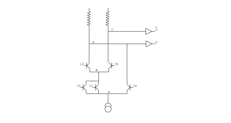
Legal circuits will never split current between paths, except for the special OR configuration where several transistors reconverge the currents immediately. Figure 2 shows an example gate where currents can split between the OR configured transistors connected to
i
0andi
1, but reconvergeimmediately.
Current may be routed through more than one level of differential pairs and then finally to a resistor. The presence or absence of current through this resistor determines the voltage across it. This voltage is propagated to the output of the gate using a driver called an Emitter Follower. Figure 2 shows a gate that implements the function
F
=(i
0+i
1)i
2. Ifi
0 andi
1are 0, current isx (v=1) Vr (v=0.5) i
[image:7.612.129.523.109.259.2]current source
Figure 1: Current Steering
O
therefore goes low. There is no current through the other resistor, soO
is pulled high. If eitheri
0ori
1is 1, then current is routed instead from point A to point B. Ifi
2is 1, the current will go toD. Otherwise, it will go to C, pulling it low and setting
O
low. IfO
is low, then there is no current through D so it is high andO
is high.In the most general case, ECL allows n-way current steering, not just 2-way current steering. Current can never be split between paths except in the OR configuration. Thus, the designer must ensure that no two inputs in the n-way comparison are high at the same time, or the circuit will malfunction. In addition to n-way splitting, ECL allows more than two resistors, corresponding to more than two outputs. However, only one output can be low at any given time due to the fact that current can only be routed through one resistor at a time. We have chosen to restrict ourselves to 2-way current steering with two resistors. This allows us to use single inputs (or ORs of inputs) that are compared to a reference voltage, avoiding the problem of ensuring mutual exclusion. We also choose to only have two outputs per gate, the true and complement values of the function.
ECL families allow the current to pass through a certain number of levels of differential pairs before it gets to a resistor. Each level has a voltage drop associated with it, so the power supply voltage for the chip determines the maximum number of levels that will fit. In our technology we normally use two levels, although a third level is allowed for situations where no reference voltage is needed. To keep things simple, only two levels are used for our automatically generated circuits.
i0 i1 Vr Vr i2
O O
A B
[image:8.612.121.524.107.322.2]C D
Figure 2: gate for
F
=(i
0+i
1)i
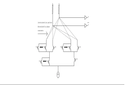
2this gate by deleting inputs and connecting up the resistors differently. The top of each current path can be connected to either of the resistors (but not both). This gives us much flexibility in terms of the logic functions we can implement. When two current paths are connected to the same resistor, it effectively creates an OR of those paths.
We can describe this general gate using boolean logic. There are two sorts of parameters for this description. Phase constants, denoted
n, select among various wiring patterns and circuit forms.These cannot be changed once the gate is implemented. Input variables, denoted
x
n, are inputs tothe the gate and of course change during gate operation. The general circuit form is:
F
(x
0;:::;x
29)=mux
(S
x;
yS
y;
zS
z)
where
S
x=
x
0+:::
+x
9S
y=
x
10+:::
+x
19S
z=
x
20+:::
+x
29and
mux
(a;b;c
)=a
b
+a
c
i0
Vr Vr
O
O
i9
Vr
i11 i19 i20 i29
Interconnection pattern
determined by phase
[image:9.612.127.525.110.383.2]constants
Figure 3: 30 input ECL gate
3
Previous Work
Technology mapping takes a network and maps it into a gate netlist. Part of the process carves out subnetworks and tries to map them to a gate. Two main approaches are used to do this mapping. Tree matching[3, 5] has been traditional, but current work is concentrated in the area of boolean matching[2]. Boolean matching looks not at the shape of a subnetwork, but rather at the logic function it implements. A gate is chosen based on this logic function, or failure is reported if no single gate can implement the function. The technology mapping algorithm repeatedly asks the boolean matcher to find possible covers of subnetworks, and uses these results to select a good cover for the entire network.
Another system[7] does technology mapping for ECL. That system, however, uses gates in a library rather than a general circuit form, restricting the quality of the output. We are unaware of any system that uses a boolean matching approach to map full-custom ECL gates.
see if we can put it into our general gate form. This is much faster for two reasons: the complexity of our algorithm is less than other boolean matching algorithms, and our algorithm matches against a single circuit form rather than requiring a large number of matches against different circuit forms.
4
Matching Algorithm
In this section, we describe an efficient algorithm to check whether a Boolean function
F
can be decomposed to our full-custom ECL circuit form. We assume that all Boolean function manipulations are performed using Boolean Decision Diagrams (BDDs) [1].4.1
Notation
Let(
x
1;:::;x
n)be
n
Boolean variables. LetX
be a set of literals, i.e. a subset offx
1;x
1;x
2;x
2;:::;x
n;x
ng.
In what follows we suppose that a set of literals never contains a variable and its negation.
s
X= P
x2X
x
denotes the disjunction of all the literals contained in
X
. Its negation,s
X,denotes the cube
Q x2X
x
.
var
(X
)denotes the set of variables appearing inX
. For example ifX
=fx
1;x
3;x
5gthenvar
(X
)=fx
1;x
3;x
5g.By extension, if
x
is a literal,var
(x
)denotes the variable from whichx
is derived.mux
(a;b;c
)denotes the Boolean functiona
b
+a
c
.
form
(F
) is a boolean predicate that is true if and only ifF
is a sum or a cube. Whenform
(F
)is true,Fand
X
F will denote respectively a Boolean constant and a set of literalsthat are such that
F
= Fs
XF
.
4.2
Description of the Algorithm
The matching algorithm itself is simple. The main problem is to prove that it detects exactly the functions of the form
F
(x
1;:::;x
n
)=
mux
(s
X;
Ys
Y;
Zs
Z). The difficulty resides in the
fact that we cannot suppose that
var
(X
),var
(Y
)andvar
(Z
)are mutually disjoint without limitingthe expressive power of the decomposition.
Here is an example. Let
F
(a;x;y;z
1;z
2)=ay
+a
(x
+z
1z
2). As written,F
is not decomposedin the required form. However
F
can be rewritten as follows:F
(a;x;y;z
1;z
2) =mux
(a
+x;
0(a
+y
);
1(z
1+z
2)), which is an acceptable decomposition.F
does not have any suchAlgorithm
Input: A Boolean function
F
(x
1;:::;x
n)
Output: If it exists, a triplet (
F
X
;F
Y;F
Z) of boolean functions such that
F
(x
1;:::;x
n) =
mux
(F
X
;F
Y;F
Z) where
F
X is a sum of literals,
form
(F
Y
)is true and
form
(F
Z) is
true.
1. Compute the cofactor
F
xfor every literalx
.2. Group the literals by equivalence classes; two literals
x
andx
0are considered to be equivalent if
F
x=
F
x0.
3. For every equivalence class
X
do:(a) Let
x
be any element of the equivalence classX
. LetF
Y be the Boolean functionF
x.If
form
(F
Y)is not true, skip to the next equivalence class.
(b) If
form
(F
sX
)is true, return the result(
s
X
;F
Y;F
s X).
(c) Compute the set
X
0of literals
v
satisfying the following two properties:var
(v
) 2var
(F
Y)and
F
v=(
F
Y) v.
(d) If
form
(F
sX[X 0
)is true, then return the result(
s
X[X0
;F
Y;F
sX[X 0
)
4. For every literal
x
do: (a) Ifform
(F
x
)is not true, skip to the next literal.
(b) Repeat steps 3c and 3d with
X
=;andF
Y=
Fx(
x
+s
XFx).
5. If all literals and equivalence classes have been processed without finding a solution,
F
cannot be decomposed as desired.4.3
Time Complexity
The cofactor of a BDD by a literal has time complexity
O
(N
) whereN
is the number of BDDnodes. The most expensive step of the algorithm is step 3c, which may require up to
O
(n
2)
cofactor computations in total. The worst-case complexity of the algorithm is thus
O
(n
2N
).We do not expect the worst-case complexity to be attained often. Equivalence classes and the test
var
(v
)2var
(F
Y)act as a filter, reducing the term
O
(n
2). Moreover
F
Y hasj
X
jfewer variablesthan
F
and is likely to have a smaller BDD representation.4.4
Proof of Correctness
Lemma 4.1 Let
F
andF
Y be two Boolean functions andX
0a set of literals such that for eachv
inX
0we haveF
v =(F
Y )
v. Then
F
=
mux
(s
X0
;F
Y;F
s X0Proof
LetG
=mux
(s
X0
;F
Y;F
s X0
). We only need to prove that
F
=G
whens
X0=1. Let
v
be a literal in
X
0. By hypothesis, we have:F
v =(F
Y )
v. On the other hand by definition of
G
wehave
G
v =(F
Y )
v. Thus for every literal in
X
0we haveF
v =G
vwhich proves that
F
=G
.Theorem 4.2 Every solution found by the algorithm is a valid decomposition of
F
.Proof
In step 3b, 3d and 4b of the algorithm, the pairs(F
Y;X
0=
X
),(F
Y;X
0=
X
[X
0)and (
F
Y
;X
0=
X
[X
0)satisfy the hypothesis of lemma 4.1. Moreover the decompositions are returned
by the algorithm only if
form
(F
Y)and
form
(F
sX0
)are both true. Thus the algorithm only returns
valid decompositions of
F
.Lemma 4.3 Let
F
be such thatF
=mux
(s
X
;F
Y;F
Z)and
form
(F
Z)true. Let
X
0 be a setof literals containing
X
and such that for every literalv
inX
0 we haveF
v = (F
Y )
v. Then
F
=mux
(s
X0
;F
Y;F
s X0)and
form
(F
sX0
)is true.
Proof
Lemma 4.1 implies thatF
=mux
(s
X0
;F
Y;F
sX0
). Since
X
0containsX
we haveF
sX 0 = (F
Z ) sX0. By hypothesis
F
Z is a cube or a sum; therefore the cofactor ofF
Z by the cubes
X0is alsoa cube or a sum, which proves that
form
(F
sX0
)is true.
Lemma 4.4 Let
F
be such thatF
=mux
(s
X
;F
Y;F
Z). Let
X
1 =fv
2X;var
(v
)62var
(F
Y)g
and
X
2=fv
2X;var
(v
)2var
(F
Y)g. Then the following assertions hold:
(i) if
X
16=;,X
1is contained in a unique equivalence classX
eq.(ii) if
X
0= f
v;var
(v
) 2var
(F
Y)and
F
v= (
F
Y) v
g as in step 3d of the algorithm, then
X
2X
0.
Proof
(i) Letv
be an element ofX
1. Sincevar
(v
) does not belong tovar
(F
Y), we have
F
v =(F
Y )
v =
F
Y. Thus all cofactors of
F
by elements ofX
1are equal to the same function,F
Y,which proves that
X
1 is a subset of an equivalence class. IfX
1is not empty, then this equivalenceclass is unique.
(ii) By definition, every element
v
ofX
2 is such thatvar
(v
) 2var
(F
Y). Moreover since
X
2X
we haveF
v=(
F
Y)
v which proves that
v
belongs toX
0.
Lemma 4.5 Let
F
=mux
(s
X
;F
Y;F
Z)be such that
form
(F
Y) and
form
(F
Z)are true. Let
X
1,X
2 andX
0be as in lemma 4.4. We suppose that
X
1 6= ;. LetX
eq be the equivalence class
containing
X
1 andx
an element ofX
1. ThenF
Y =F
xand when the algorithm is processing the
equivalence class
X
eq:if
X
2=;the algorithm returns the valid decompositionmux
(s
Xeq
;F
x;F
s Xeq)in step 3b. if
X
2 6=;the algorithm returns the valid decompositionmux
(s
X eq
[X 0
;F
x
;F
s Xeq[X0 )in step
Proof
IfX
2 =;, apply lemma 4.1 withF
Y=
F
xand
X
0 =X
eq. If
X
26=;, apply lemma 4.1
with
F
Y =F
xand
X
0 =X
eq [
X
0
. Lemma 4.4 shows that in both cases
X
X
0. Lemma 4.3concludes the proof.
Lemma 4.6 Let
F
=mux
(s
X
;F
Y;F
Z)be such that
form
(F
Y) and
form
(F
Z)are true. Let
X
1,X
2 andX
0be as in lemma 4.4. We suppose that
X
1 =;. If one exists, letx
be an elementof
X
2 appearing in negated form inX
FY. LetX
0be as in lemma 4.4. Then
F
Y =Fx
(
x
+s
XF x)and when the algorithm processes the literal
x
in step 4b it returns the valid decompositionmux
(s
X0
;
Fx
(
x
+s
X Fx );F
s X 0 ).Proof
We haveF
x =(F
Y )
x. Since
form
(F
Y
)is true,
form
(F
x)is also true. Thus(
F
Y ) x =F
x = F xs
X Fx. By hypothesis,
x
appears in negated form ins
X FY
, thus
F
Y =F x
(
x
+s
XFx ).
From lemma 4.1, we deduce that
F
=mux
(s
X0
;F
Y;F
sX 0
). Since
X
1=;, we haveX
=X
2X
0. We conclude with lemma 4.3 that
form
(F
s X
0
)is true.
Theorem 4.7 If a solution exists, it is found and returned.
Proof
The only case not covered by the lemmas 4.5 and 4.6 is the case whereX
1 = ;and allliterals in
X
2appear inF
Y unnegated. However in that caseF
Y=
(s
X+
s
Y)for some set of
literals
Y
, which means thatF
Y can be replaced by the constantandF
=
mux
(s
X
;;F
Z ). Thiscase is handled by step 3b of the algorithm.
5
Experimental Results
We have chosen three blocks of control equations from our current processor design.
Characteristics of these three blocks are shown in Table 1. The first block is the major
control block in our design, controlling the integer and floating point datapaths. The other
two are small blocks typical of the rest of the design.
Table 2 shows the results of mapping. Most gates are small, with fanins of 5 or less.
Much of this is the result of small equations in the original design specification. Many
equations are simple, in that they combine only a few variables or just pass data from one
pipe stage to the next. Timing verification has shown us, however, that the critical path of
the design contains more complex logic, so it is important that our mapping algorithm find
good solutions. It is worth noting that the maximum fanin of the gates produced by our
circuit # eqns # lits lit/eqn
[image:14.612.242.406.116.173.2]Control 2319 9834 4.2 FPACtl 71 141 1.99 FPDivCtl 43 86 2.0
Table 1: Examples Used
circuit # gates gate/eqn fanin max fanin
[image:14.612.210.442.230.287.2]Control 3534 1.53 2.89 22 FPACtl 71 1.00 2.06 8 FPDivCtl 43 1.00 2.05 5
Table 2: Performance of Full Algorithm
circuit # gates gate/eqn fanin max fanin time
Control 3575 1.54 2.87 22 0.98 FPACtl 73 1.03 2.01 8 1.04 FPDivCtl 43 1.00 2.05 5 1.02
Table 3: Eliminating Steps 3d and 4
circuit # gates gate/eqn fanin max fanin time
[image:14.612.192.458.453.511.2]Control 5773 2.50 2.16 5 1.15 FPACtl 92 1.30 1.80 5 1.50 FPDivCtl 43 1.00 2.05 5 0.99
Table 4: Limited Mapping
# eqns: number of equations in the circuit
# lits: number of uses of literals in factored form
lit/eqn: average number of literals per equation
# gates: number of gates produced by the algorithm
gate/eqn: average number of gates per equation
fanin: average gate fanin
max fanin: maximum gate fanin
We experimented with two variants of the algorithm, based on observation of the
algorithm’s behavior on our three examples. We observed that 98.6% of the solutions found
were found in step 3b of the algorithm, and all the remaining solutions were found in step
3d. Step 4 was not needed for any of our examples, although we can construct artificial
examples that do require step 4.
Based upon this data, we tried eliminating steps 3c, 3d and 4 from our algorithm. Table
3 shows the results. CPU time is essentially unchanged, while the number of gates needed
has gone up slightly. It is important to note that when the algorithm misses a match, the
algorithm will be called again on a smaller piece of logic. Thus, matching is tried over and
over on different pieces until a match is found. A faster algorithm that misses matches can
actually result in longer run times and poorer results.
Another variant we tried was to limit the mapped functions to
F
=mux
(F
x
;F
y;F
z ),
where
F
x,
F
y, and
F
zhave disjoint support sets. In this case, we know that the function’s
variables partition into no more than six equivalence classes. We combine steps 1 and 2 of
the algorithm, computing equivalence classes as we go. We can terminate our computation
early if more than 6 are found. In addition, in step 3 we pick the equivalence class with
the most members, rather than iterating over all equivalence classes. This results in an
algorithm that terminates early on complicated cases. Table 4 shows that this is a poor
choice. The algorithm misses so many matches that the total runtime increases and the
results become poorer.
6
Conclusion and Future Work
We have demonstrated a technology mapper for full-custom ECL gates. The technology
mapper takes advantage of the high fanin and regular structure of these gates to implement
each equation using a small number of gates. The algorithm proceeds using efficient
operations on BDDs, producing a mapping in an acceptable amount of time.
Not described in this paper are electrical optimizations on the gates produced. These
optimizations include separate power sizing of the logic portion of the gate and the output
driver. This power sizing is done by starting with low power everywhere, and then walking
over the graph of gates and wires increasing the power along the critical path.
Trial
account during the power adjustment phase.
Additional optimizations change voltage
swings and convert signals to differential pairs when it is possible given the choice of
gates. Certain gates, such as those with a large number of OR terms at the bottom, can be
best implemented using a slightly different circuit called a level-shifting-OR, so we have a
pattern matching and replacement phase to take care of this and similar optimizations.
Future extensions to the mapper described here could look at a number of factors. The
delay through an ECL gate is not the same for each input, so it makes a difference to which
input a variable is assigned. In order to take this into account in our algorithm, we would
have to have available the arrival times of the individual inputs and a model for gate delay.
7
Acknowledgments
We would like to thank Hamid Savoj for his help, as well as Jeremey Dion, Ramsey Haddad,
and Louis Monier of Digital Equipment Corporation’s Western Research Laboratory. In
addition, Ramsey Haddad deserves credit for the initial implementation of our BDD package.
References
[1] R. E. Bryant. Graph Based Algorithms for Boolean Function Manipulation. IEEE Transactions
on Computers, C-35(8):677–691, August 1986.
[2] J. R. Burch and D. E. Long. Efficient Boolean Function Mapping. In Proc. of the ICCAD-92, pages 408–411, November 1992.
[3] E. Detjens, G. Gannot, R. Rudell, A. Sangiovanni-Vincentelli, and A. Wang. Technology Mapping in MIS. In Proc. of the ICCAD-87, pages 116–119, November 1987.
[4] N. Jouppi, P. Boyle, J. Dion, J. Doherty, A. Eustace, R. Haddad, R. Mayo, S. Menon, L. Monier, D. Stark, S. Turrini, and L. Yang. A 300MHz 115W 32b Bipolar ECL Microprocessor with On-Chip Caches. In IEEE International Solid-State Circuits Conference, February 1993. [5] K. Keutzer. DAGON: Technology Binding and Local Optimization by DAG Matching. In
Proceedings of the 24th Design Automation Conference, pages 341–347. ACM/IEEE, June
1987.
[6] L. Monier and J. Dion. Design Tools for BIPS-0. Technical Report TN-32, Digital Equipment Corporation. Western Research Laboratory, December 1992.
[7] V. Morgan and D. Gregory. An ECL Logic-Synthesis System. In 28st ACM/IEEE Design
WRL Research Reports
‘‘Titan System Manual.’’ ‘‘MultiTitan: Four Architecture Papers.’’
Michael J. K. Nielsen. Norman P. Jouppi, Jeremy Dion, David Boggs,
Mich-WRL Research Report 86/1, September 1986. ael J. K. Nielsen.
WRL Research Report 87/8, April 1988. ‘‘Global Register Allocation at Link Time.’’
David W. Wall. ‘‘Fast Printed Circuit Board Routing.’’
WRL Research Report 86/3, October 1986. Jeremy Dion.
WRL Research Report 88/1, March 1988. ‘‘Optimal Finned Heat Sinks.’’
William R. Hamburgen. ‘‘Compacting Garbage Collection with Ambiguous
WRL Research Report 86/4, October 1986. Roots.’’ Joel F. Bartlett.
‘‘The Mahler Experience: Using an Intermediate WRL Research Report 88/2, February 1988. Language as the Machine Description.’’
David W. Wall and Michael L. Powell. ‘‘The Experimental Literature of The Internet: An WRL Research Report 87/1, August 1987. Annotated Bibliography.’’
Jeffrey C. Mogul.
‘‘The Packet Filter: An Efficient Mechanism for WRL Research Report 88/3, August 1988. User-level Network Code.’’
Jeffrey C. Mogul, Richard F. Rashid, Michael ‘‘Measured Capacity of an Ethernet: Myths and
J. Accetta. Reality.’’
WRL Research Report 87/2, November 1987. David R. Boggs, Jeffrey C. Mogul, Christopher A. Kent.
‘‘Fragmentation Considered Harmful.’’ WRL Research Report 88/4, September 1988. Christopher A. Kent, Jeffrey C. Mogul.
WRL Research Report 87/3, December 1987. ‘‘Visa Protocols for Controlling Inter-Organizational Datagram Flow: Extended Description.’’
‘‘Cache Coherence in Distributed Systems.’’ Deborah Estrin, Jeffrey C. Mogul, Gene Tsudik,
Christopher A. Kent. Kamaljit Anand.
WRL Research Report 87/4, December 1987. WRL Research Report 88/5, December 1988.
‘‘Register Windows vs. Register Allocation.’’ ‘‘SCHEME->C A Portable Scheme-to-C Compiler.’’
David W. Wall. Joel F. Bartlett.
WRL Research Report 87/5, December 1987. WRL Research Report 89/1, January 1989.
‘‘Editing Graphical Objects Using Procedural ‘‘Optimal Group Distribution in Carry-Skip
Ad-Representations.’’ ders.’’
Paul J. Asente. Silvio Turrini.
WRL Research Report 87/6, November 1987. WRL Research Report 89/2, February 1989.
‘‘The USENET Cookbook: an Experiment in ‘‘Precise Robotic Paste Dot Dispensing.’’
Electronic Publication.’’ William R. Hamburgen.
Brian K. Reid. WRL Research Report 89/3, February 1989.
‘‘Simple and Flexible Datagram Access Controls for ‘‘Link-Time Code Modification.’’
Unix-based Gateways.’’ David W. Wall.
Jeffrey C. Mogul. WRL Research Report 89/17, September 1989.
WRL Research Report 89/4, March 1989.
‘‘Noise Issues in the ECL Circuit Family.’’ ‘‘Spritely NFS: Implementation and Performance of
Jeffrey Y.F. Tang and J. Leon Yang. Cache-Consistency Protocols.’’
WRL Research Report 90/1, January 1990. V. Srinivasan and Jeffrey C. Mogul.
WRL Research Report 89/5, May 1989.
‘‘Efficient Generation of Test Patterns Using Boolean Satisfiablilty.’’
‘‘Available Instruction-Level Parallelism for
Super-Tracy Larrabee. scalar and Superpipelined Machines.’’
WRL Research Report 90/2, February 1990. Norman P. Jouppi and David W. Wall.
WRL Research Report 89/7, July 1989.
‘‘Two Papers on Test Pattern Generation.’’ Tracy Larrabee.
‘‘A Unified Vector/Scalar Floating-Point
Architec-WRL Research Report 90/3, March 1990. ture.’’
Norman P. Jouppi, Jonathan Bertoni, and David
‘‘Virtual Memory vs. The File System.’’ W. Wall.
Michael N. Nelson. WRL Research Report 89/8, July 1989.
WRL Research Report 90/4, March 1990. ‘‘Architectural and Organizational Tradeoffs in the
‘‘Efficient Use of Workstations for Passive Monitor-Design of the MultiTitan CPU.’’
ing of Local Area Networks.’’ Norman P. Jouppi.
Jeffrey C. Mogul. WRL Research Report 89/9, July 1989.
WRL Research Report 90/5, July 1990. ‘‘Integration and Packaging Plateaus of Processor
‘‘A One-Dimensional Thermal Model for the VAX Performance.’’
9000 Multi Chip Units.’’ Norman P. Jouppi.
John S. Fitch. WRL Research Report 89/10, July 1989.
WRL Research Report 90/6, July 1990. ‘‘A 20-MIPS Sustained 32-bit CMOS
Microproces-‘‘1990 DECWRL/Livermore Magic Release.’’ sor with High Ratio of Sustained to Peak
Perfor-Robert N. Mayo, Michael H. Arnold, Walter S. Scott, mance.’’
Don Stark, Gordon T. Hamachi. Norman P. Jouppi and Jeffrey Y. F. Tang.
WRL Research Report 90/7, September 1990. WRL Research Report 89/11, July 1989.
‘‘Pool Boiling Enhancement Techniques for Water at ‘‘The Distribution of Instruction-Level and Machine
Low Pressure.’’ Parallelism and Its Effect on Performance.’’
Wade R. McGillis, John S. Fitch, William Norman P. Jouppi.
R. Hamburgen, Van P. Carey. WRL Research Report 89/13, July 1989.
WRL Research Report 90/9, December 1990. ‘‘Long Address Traces from RISC Machines:
‘‘Writing Fast X Servers for Dumb Color Frame Buf-Generation and Analysis.’’
fers.’’ Anita Borg, R.E.Kessler, Georgia Lazana, and David
Joel McCormack. W. Wall.
‘‘A Simulation Based Study of TLB Performance.’’ ‘‘Cache Write Policies and Performance.’’ J. Bradley Chen, Anita Borg, Norman P. Jouppi. Norman P. Jouppi.
WRL Research Report 91/2, November 1991. WRL Research Report 91/12, December 1991. ‘‘Analysis of Power Supply Networks in VLSI
Cir-‘‘Packaging a 150 W Bipolar ECL Microprocessor.’’ cuits.’’
William R. Hamburgen, John S. Fitch. Don Stark.
WRL Research Report 92/1, March 1992. WRL Research Report 91/3, April 1991.
‘‘Observing TCP Dynamics in Real Networks.’’ ‘‘TurboChannel T1 Adapter.’’
Jeffrey C. Mogul. David Boggs.
WRL Research Report 92/2, April 1992. WRL Research Report 91/4, April 1991.
‘‘Systems for Late Code Modification.’’ ‘‘Procedure Merging with Instruction Caches.’’
David W. Wall. Scott McFarling.
WRL Research Report 92/3, May 1992. WRL Research Report 91/5, March 1991.
‘‘Piecewise Linear Models for Switch-Level Simula-‘‘Don’t Fidget with Widgets, Draw!.’’
tion.’’ Joel Bartlett.
Russell Kao. WRL Research Report 91/6, May 1991.
WRL Research Report 92/5, September 1992. ‘‘Pool Boiling on Small Heat Dissipating Elements in
Water at Subatmospheric Pressure.’’
Wade R. McGillis, John S. Fitch, William ‘‘A Practical System for Intermodule Code
Optimiza-R. Hamburgen, Van P. Carey. tion at Link-Time.’’
WRL Research Report 91/7, June 1991. Amitabh Srivastava and David W. Wall. WRL Research Report 92/6, December 1992. ‘‘Incremental, Generational Mostly-Copying
Gar-bage Collection in Uncooperative Environ- ‘‘A Smart Frame Buffer.’’
ments.’’ Joel McCormack & Bob McNamara.
G. May Yip. WRL Research Report 93/1, January 1993.
WRL Research Report 91/8, June 1991.
‘‘Recovery in Spritely NFS.’’ ‘‘Interleaved Fin Thermal Connectors for Multichip Jeffrey C. Mogul.
Modules.’’ WRL Research Report 93/2, June 1993.
William R. Hamburgen.
WRL Research Report 91/9, August 1991. ‘‘Tradeoffs in Two-Level On-Chip Caching.’’ Norman P. Jouppi & Steven J.E. Wilton. ‘‘Experience with a Software-defined Machine Ar- WRL Research Report 93/3, October 1993.
chitecture.’’
David W. Wall. ‘‘Unreachable Procedures in Object-oriented
WRL Research Report 91/10, August 1991. Programing.’’ Amitabh Srivastava.
‘‘Network Locality at the Scale of Processes.’’ WRL Research Report 93/4, August 1993. Jeffrey C. Mogul.
WRL Research Report 91/11, November 1991. ‘‘Limits of Instruction-Level Parallelism.’’ David W. Wall.
‘‘Fluoroelastomer Pressure Pad Design for Microelectronic Applications.’’
Alberto Makino, William R. Hamburgen, John S. Fitch.
WRL Research Report 93/7, November 1993.
WRL Technical Notes
‘‘TCP/IP PrintServer: Print Server Protocol.’’ ‘‘Predicting Program Behavior Using Real or Es-Brian K. Reid and Christopher A. Kent. timated Profiles.’’
WRL Technical Note TN-4, September 1988. David W. Wall.
WRL Technical Note TN-18, December 1990. ‘‘TCP/IP PrintServer: Server Architecture and
Im-plementation.’’ ‘‘Cache Replacement with Dynamic Exclusion’’
Christopher A. Kent. Scott McFarling.
WRL Technical Note TN-7, November 1988. WRL Technical Note TN-22, November 1991.
‘‘Smart Code, Stupid Memory: A Fast X Server for a ‘‘Boiling Binary Mixtures at Subatmospheric
Pres-Dumb Color Frame Buffer.’’ sures’’
Joel McCormack. Wade R. McGillis, John S. Fitch, William
WRL Technical Note TN-9, September 1989. R. Hamburgen, Van P. Carey.
WRL Technical Note TN-23, January 1992. ‘‘Why Aren’t Operating Systems Getting Faster As
Fast As Hardware?’’ ‘‘A Comparison of Acoustic and Infrared Inspection
John Ousterhout. Techniques for Die Attach’’
WRL Technical Note TN-11, October 1989. John S. Fitch.
WRL Technical Note TN-24, January 1992. ‘‘Mostly-Copying Garbage Collection Picks Up
Generations and C++.’’ ‘‘TurboChannel Versatec Adapter’’
Joel F. Bartlett. David Boggs.
WRL Technical Note TN-12, October 1989. WRL Technical Note TN-26, January 1992.
‘‘The Effect of Context Switches on Cache Perfor- ‘‘A Recovery Protocol For Spritely NFS’’
mance.’’ Jeffrey C. Mogul.
Jeffrey C. Mogul and Anita Borg. WRL Technical Note TN-27, April 1992. WRL Technical Note TN-16, December 1990.
‘‘Electrical Evaluation Of The BIPS-0 Package’’ ‘‘MTOOL: A Method For Detecting Memory Bot- Patrick D. Boyle.
tlenecks.’’ WRL Technical Note TN-29, July 1992.
Aaron Goldberg and John Hennessy.
‘‘Transparent Controls for Interactive Graphics’’ WRL Technical Note TN-17, December 1990.
Joel F. Bartlett.
‘‘Design Tools for BIPS-0’’ Jeremy Dion & Louis Monier.
WRL Technical Note TN-32, December 1992. ‘‘Link-Time Optimization of Address Calculation on
a 64-Bit Architecture’’
Amitabh Srivastava and David W. Wall. WRL Technical Note TN-35, June 1993.
‘‘Combining Branch Predictors’’ Scott McFarling.
WRL Technical Note TN-36, June 1993.
‘‘Boolean Matching for Full-Custom ECL Gates’’ Robert N. Mayo and Herve Touati.