N A N O E X P R E S S
Open Access
Design High-Efficiency III
–
V Nanowire/Si
Two-Junction Solar Cell
Y Wang
1, Y Zhang
1, D Zhang
1*, S He
1and X Li
2*Abstract
In this paper, we report the electrical simulation results of a proposed GaInP nanowire (NW)/Si two-junction solar cell. The NW physical dimensions are determined for optimized solar energy absorption and current matching between each subcell. Two key factors (minority carrier lifetime, surface recombination velocity) affecting power conversion efficiency (PCE) of the solar cell are highlighted, and a practical guideline to design high-efficiency two-junction solar cell is thus provided. Considering the practical surface and bulk defects in GaInP semiconductor, a promising PCE of 27.5 % can be obtained. The results depict the usefulness of integrating NWs to construct high-efficiency multi-junction III–V solar cells.
Keywords:Two-junction solar cells; Nanowire; Current matching; Photovoltaics
Background
Multi-junction solar cells are constituted by series-connected multiple semiconductor layers (subcells) to convert the energy of light directly into electricity by the photovol-taic effect. By dividing the broad solar spectrum into smaller sections, the multi-junction solar cell can con-vert solar energy more efficiently. Till now, efficiencies exceeding 44 % have been achieved at high concentra-tion ratios for convenconcentra-tional triple-juncconcentra-tion cell cells [1]. However, the high efficiency of thin-film multi-junction solar cell is gained at the cost of increased complexity and manufacturing price. The development of high-efficiency, low-cost photovoltaic device is urgently needed.
Due to their potential to realize low-cost and high energy conversion efficiency solar cells, semiconductor nanowire array (NWA) is a topic of intense research for photovoltaic applications. Recently, many theoretical and experimental works, which are focused on the design of single III–V NWAp-njunction, are widely reported [2, 3]. Meanwhile, some axially connected nanowire two-junction cells are also theoretically designed to obtain high-efficiency solar cells [4]. Considering the fact that many kinds of III–V NWAs have been successfully prepared on hetero-substrates (such as Si) [5], the concept of multi-junction
solar cell can also be used in the design of photovoltaic de-vices. As compared with conventional multi-junction solar cell, the integration of NWAs in photovoltaic applications has the following merits. Firstly, NWA with well-defined geometrical structures exhibits higher light absorption than their thin-film counterparts of the same thickness, due to the integration of NWA in solar cells significantly changes the mechanism of light absorption [6]. Secondly, when the top NWA cell is designed in radialp-nstructure, the short collection lengths facilitate the efficient collection of photo-generated carriers, and herein, the Shockley-Quisser effi-ciency limit for nanowire arrays is higher than for the conventional thin film [7]. Finally, the integration of semi-conductor NWA on low-cost substrates can help substan-tially reduce the final cost of PV fabrication.
In view of this, we have recently presented a study on two-junction III–V NWA/Si solar cell, which is con-sisted by III–V NWA withp-njunction on the active Si substrate. We show that outstanding light harvesting rooted from the strong light trapping and the formation of Fabry-Pérot optical cavity in the NWA enables the cell to produce high photocurrent [8]. In this paper, we further report the electrical performance via simulation, where the physical dimensions are taken by considering the condition of current matching and maximized solar energy absorption. The impact of III–V NWA quality in terms of minority carrier lifetime, surface recombination velocity (SRV) on the solar cell performance is presented,
* Correspondence:[email protected];[email protected]
1College of Electrical Engineering and Automation, Anhui University, Hefei,
China
2Key Laboratory of Material Physics, Institute of Solid State Physics, Chinese
Academy of Sciences, Hefei 230031, China
rials, in this study, we fixed the length (L) of GaInP NW at 2μm. The NWA cell was connected with Si thin-film cell by the tunnel junction which can be assumed to be per-fect. The SiO2layer is added between the shell of NWs and the Si substrate. Transparent conductive oxide (TCO) and metal contacts are placed at the top and bottom of the structure.
The optical properties of GaInP NWA/Si solar cells are investigated using Sentaurus Electromagnetic Wave Solver module package, a finite-difference time-domain (FDTD) full field electromagnetic simulation tool [11]. In order to simplify the calculation, the Si thin film is as-sumed infinite thick with no transmission loss by using a perfect match layer (PML) adjacent underneath the Si film. To investigate the potential photovoltaic efficiency of top NWA solar cells, a coupled optoelectronic simula-tion is presented. Based on the posisimula-tion-dependent light absorption obtained by FDTD simulation, the three-dimensional (3D) carrier generation rate is obtained from the divergence of the Poynting vector. The current-voltage behaviors of the GaInP NWA subcells are calcu-lated at three-dimensional by using the weighted optical generation profiles [12]. The electrical behaviors of the bottom Si cell are calculated at two-dimensional with Beer-Lambert absorption model while a reflection loss
Current Matching Process
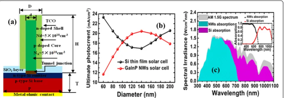
Figure 1b shows the ultimate photocurrent as a function of NW diameters from 60 to 200 nm. One can find the photocurrents of the two subcells match each other closely at the NW diameters of 100 and 180 nm. For hetero-epitaxial growth of GaInP NWs on silicon sub-strate, larger diameter of NWs means more dislocations form at the interface of hetero-structure [13]. Hence, in the following electrical simulation, the radialp-njunction (core diameter of 60 nm, shell diameter (D) of 100 nm, the filling ratio (D/P) of 0.5, periodicity (P) of NW unit 200 nm) is chosen. Figure 1c shows the absorption of NWA with NW diameter of 100 nm and Si film under AM1.5G illumination. One can find that above 90 % inci-dent light is absorbed by this NWA/Si substrate structure, which implies the high absorption capacity of the pro-posed two-junction solar cell. Furthermore, the aforemen-tioned discussion also indicates that with fixed subcell thickness, the condition of current matching in the III–V NW/Si multi-junction can be fulfilled by adjusting the diameter of the NWs. Such an optimization process for current matching differs greatly from that in conventional multi-junction cells in which an anti-reflection coating de-sign combined with subcell thickness adjustments should be used.
[image:2.595.59.540.527.693.2]Minority Carrier Lifetimes
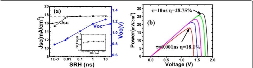
The minority carrier diffusion length determines the PCE in such a way that it affects the photogenerated car-rier collection and, hence, the short-circuit current (Jsc) and the open-circuit voltage (Voc) and fill factor (FF). To examine the effects of the densities of mid-band gap trap state on the photogenerated carrier collection of the top NWA solar cell, we have performed simulations with SRH minority carrier lifetimes (τSRH) ranging from 10−12 to 10−8 s, which reflects varying the densities of mid-band gap trap state. Figure 2a and its inset show the variation of simulatedVocand the Jsc and FF with τSRH. One can find Voc decrease substantially from 1.28 to 0.81 V whenτSRHvaries from 10 ns to 1 ps. This result agrees well with that reported by Kayes et. al., who pre-sented the degree to which the open-circuit voltage var-ied with the trap density depended most strongly on the trap density in the depletion region [14]. The FF was kept above 0.86 as τSRH > 7 × 10⁻⁸s. In the case that τSRH= 1 × 10⁻¹² s, the FF undergo only a tiny decrease to 0.839. This tiny drop may be attributed to series in-trinsic resistance enhancement caused by high defect density under low minority carrier lifetimes. When the τSRH = 10 ns, the Jsc of the top core-shell p-n cell is 17.7 mA/cm2. This value is very close to the calculated photocurrent (18.2 mA/cm2) of this optimized structure
as shown in Fig. 1b. Note that when the τSRHdecreases to 0.01 ns, high short current (>17.5 mA/cm2) can be maintained. In this case, above 96 % photogenerated car-rier can be effectively transported to the electrodes. These phenomena imply the high photogenerated carrier extrac-tion capabilities of this radial p-n junctional structure. Considering that the electrical current matching must be satisfied for the series-connected cell structure, the char-acter of radial NWA’sJscnot sensitive to the bulk defects is very promising for fabricating two-junction solar cells. However, whenτSRHis further decreased to 1 ps (the mi-nority hole diffusion length was estimated to be 8 nm), theJscdecreases greatly owing to the high photogenerated carrier recombination before reaching the built-in electric field region.
Figure 2b shows power of the proposed two-junction cell variation with voltage. The PCE can be found to de-crease progressively with the reduction ofτSRH. Obviously, although current matching can be easily satisfied, rela-tively lower trap densities in top GaInP NWA is needed to obtain higher PCE of the proposed two-junction cell.
Surface Recombination Velocity
The high surface-to-volume ratio represented by the adoption of a cylindrical radial junction increases both the active depletion region as well as the overall surface
Fig. 2aThe variation of simulated open-circuit voltage (Voc) and the short-circuit current (Jsc) withτSRH,black dashed lineis the calculatedJscof
the bottom Si subcell, theinsetinashows the variation of fill factor (FF) withτSRH.bPower-voltage characteristics of the III–V NWs/Si solar cells
under one sun AM1.5G illumination at variousτSRH
Fig. 3aThe variation ofVocandJscwith SRV.bTheJ-Vcharacteristic for the Si bottom cell, NW top cell, and series-connected two-junction cell
[image:3.595.58.539.89.218.2] [image:3.595.59.539.598.705.2]be described as:
RS;t ¼Ntrap
σnσpvthnvpth nsps−n2i;eff
σnvthnðnsþn1Þ þσpvthpðpsþp1Þ
ð1Þ
whereσn,pand νthn;p are respectively capture cross section and thermal velocity of electron and hole. To further sim-plify the recombination model, we assume thatσn=σp=σ
and νth
n ¼νthp ¼νth. Meanwhile, when the semiconductor is exposed to the sunlight (far from equilibrium state), for-mula (1) can be simplified to:
RS;t ¼Ntrapσvthnnsps
sþps ð2Þ
For n-type semiconductor, Rs,t=Stps where SRV St= Ntrapσvth
. In this way, one can correlate the density of surface trap states with SRV.
Figure 3a shows the variation ofVocandJscwith SRV. Voc progressively decrease with larger SRV but is rela-tively not as insensitive as to τSRH. However, when SRV increases from 0 to 5 × 106cm/s, Jsc decreases substan-tially from 17.78 to 15.56 mA/cm2. About 15 % photo-generated photocurrent annihilated, compared with the cell with perfect surface. Obviously, a large amount of photogenerated carriers recombine at the surface of NWA, due to the high surface-to-volume ratio of the proposed top NWA cells. Meanwhile, the electric field caused by band bending will drive minority carriers to migrate toward the surface. This in turn promotes surface recombination of minority carriers. Hence, in the top NWA subcell, the surface recombination is responsible for the annihilation of minority carriers and decides theJsc of the proposed NWA cell. As expected, one can find that PCE of proposed two-junction cell decrease to 24.8 %, when SRV of the top GaInP cell increased to 5 × 106cm/ s. This is because the decrease of photogenerated current in the top subcell will restrict the output current in the bottom Si active layer, considering current matching must be satisfied between the two series-connected subcells.
From the aforementioned discussion, to effectively ex-tract the photogenerated carrier and achieve high effi-ciency of the proposed two-junction cell, it is necessary to control both the bulk and surface defect densities of
than arsenic compound semiconductors such as AlGaAs and GaAs. In this case, the proposed cell yields a very promising device efficiency of 27.5 % with a short-circuit current density (Jsc) of 17.38 mA/cm2, an open-circuit voltage of 1.84 V, and a fill factor of 0.86 under the illu-mination of one sun (AM1.5G).
Conclusions
In conclusion, a device physics model incorporated with optical characteristics has been established to analyze the electrical performance of GaInP NWA/Si two-junction solar cell in term of itsJ-Vcharacteristics and, hence, the PCE. From our simulation, it is suggested that the current matching of each subcell can be fulfilled by adjusting the diameter of the top NWA cell. Furthermore, as a photo-voltaic device compromised by NWA, both SRH and SRV have great effect on the performance of the proposed solar cell. A promising PCE of 28.15 % can be obtained, considering the practical surface and bulk defects in GaInP semiconductor. This performance is comparable with that of state-of-the-art two-junction cell under one sun illumination (http://www.nrel.gov/news/press/ 2013/2226.html?print).
Abbreviations
FDTD:Finite-difference time-domain; NWA: Nanowire array; P3HT: Poly(3-hexylthiophene); PCE: Power conversion efficiency; PML: Perfect match layer.
Competing Interests
The authors declare that they have no competing interests.
Authors’Contributions
YW designed the research contents and methods. YW, YZ, DZ, and SH did the simulation work. YW, YZ, DZ, GF and XL carried out the data analysis and wrote the paper. All authors read, corrected, and approved the final manuscript.
Acknowledgements
This work was supported by the National Natural Science Foundation of China (Grant No. 51472247) and the Natural Science Foundation of Anhui province (Grant No.1308085MA10).
Received: 15 February 2015 Accepted: 2 June 2015
References
1. Green MA, Emery K, Hishikawa Y, Warta W, Dunlop ED. Solar cell efficiency tables. Prog Photovolt Res Appl. 2013;21(5):827–37.
3. Wallentin J, Anttu N, Asoli D, Huffman M, Åberg I, Magnusson MH, et al. InP nanowire array solar cells achieving 13.8% efficiency by exceeding the ray optics limit. Science. 2013;339(6123):1057–60.
4. Wang S, Yan X, Zhang X, Li J, Ren X. Axially connected nanowire core-shell pn junctions: a composite structure for high-efficiency solar cells. Nanoscale Res Lett. 2015;10(1):1–7.
5. Plissard S, Dick KA, Larrieu G, Godey S, Addad A, Wallart X, et al. Gold-free growth of GaAs nanowires on silicon: arrays and polytypism. Nanotechnology. 2010;21(38):385602.
6. Anttu N, Xu HQ. Efficient light management in vertical nanowire arrays for photovoltaics. Opt Express. 2013;21(s3):A558–75.
7. Anttu N. Shockley–Queisser detailed balance efficiency limit for nanowire solar cells. ACS Photonics. 2015;2(3):446–53.
8. Bu S, Li X, Wen L, Zeng X, Zhao Y, Wang W, et al. Optical and electrical simulations of two-junction III-V nanowires on Si solar cell. Appl Phys Lett. 2013;102(3):031106.
9. Huang N, Lin C, Povinelli ML. Limiting efficiencies of tandem solar cells consisting of III-V nanowire arrays on silicon. J Appl Phys. 2012;112 (6):064321.
10. LaPierre RR. Theoretical conversion efficiency of a two-junction III-V nanowire. J Appl Phys. 2011;110(1):014310. on Si solar cell. 11. Sentaurus TCAD Software Suite, Version D-2010.03, Synopsys Inc,
MountainView, USA, 2010.
12. Sentaurus TCAD User Guide, Version D-2010.03, Synopsys Inc, Mountain View, USA, 2010.
13. Chuang LC, Moewe M, Chase C, Kobayashi NP, Chang-Hasnain C. Critical diameter for III-V nanowires grown on lattice-mismatched substrates. Appl Phys Lett. 2007;90(4):043115.
14. Kayes BM, Atwater HA, Lewis NS. Comparison of the device physics principles of planar and radial p-n junction nanorod solar cells. J Appl Phys. 2005;97(11):114302.
15. D. T. Stevenson, R. J. Keyes.“Measurements of surface recombination velocity at germanium surfaces,”Physca, vol. 20 no. p.1041, 1954. 16. Joyce HJ, Gao Q, Tan HH, Jagadish C, Kim Y, Zhang X, et al. Twin-free
uniform epitaxial GaAs nanowires grown by a two-temperature process. Nano Lett. 2007;7(4):921–6.
17. Shtrikman H, Popovitz-Biro R, Kretinin A, Heiblum M. Stacking-faults-free zinc blende GaAs Nanowires. Nano Lett. 2009;9(1):215–9.
18. Pearton SJ, Ren F, Hobson WS, Abernathy CR, Chakrabarti UK. Comparison of surface recombination velocities in InGaP and AlGaAs mesa diodes. J Vac Sci Technol B. 1994;12(1):142.
Submit your manuscript to a
journal and benefi t from:
7Convenient online submission
7Rigorous peer review
7Immediate publication on acceptance
7Open access: articles freely available online
7High visibility within the fi eld
7Retaining the copyright to your article