N A N O I D E A
Open Access
Study on the Multi-level
Resistance-Switching Memory and
Memory-State-Dependent Photovoltage in Pt/Nd:SrTiO
3
Junctions
Shengkai Wang, Xianwen Sun
*, Guanghui Li, Caihong Jia, Guoqiang Li and Weifeng Zhang
*Abstract
Pt/Nd:SrTiO3(STO)/In devices were fabricated by depositing Schottky-contact Pt and Ohmic-contact In electrodes
on a single crystal STO with Nd doping. The Pt/Nd:STO/In devices show multi-level resistance-switching (RS) memory and memory-state-dependent photovoltage (PV) effects, which can be controlled by the applied pulse width or magnitude. Both the RS and PV are related to the bias-induced modulation of the interface barrier, both in height and width, at the Pt/Nd:STO interface. The results establish a strong connection between the RS/PV effects and the modulation of the Nd:STO interface triggered by applied electric field and provide a new route by using an open-circuit voltage for non-destructively sensing multiple non-volatile memory states.
Keywords:Resistive switching, Interface state, Multi-level memory, Photovoltage
Background
SrTiO3(STO) is a large bandgap (3.2 eV) insulator. It is
considered to be a model perovskite material due to its simple cubic structure in a wide temperature range [1]. STO has abundant photoelectric performance which can be directly manipulated via doping with a donor- or acceptor-type transition metal. The range of applications of STO system is very wide [2, 3]. Recently, STO system has received a great deal of scientific attention due to the resistive switching (RS) phenomena, which can be considered as a good candidate for building the resistive random access memory (RRAM) [4, 5].
The RS device based on STO is usually a metal/STO/ metal structure. The RS properties of STO system, i.e., from acceptor- to donor-doped STO, have been widely investigated. Different physical mechanisms have been proposed to explain the switching behavior. For acceptor-doped (e.g., Fe and Cr) STO, the works emphasize the property change in the crystal bulk, in which the RS was attributed to electric-field-driven migration of oxygen vacancy, either the fast transport of oxygen vacancies
along dislocations or the formation of oxygen-vacancy array under high electrical stress [6–11]. On the other hand, for RS device based on donor-doped (e.g., Nb) STO, the Schottky-type contact between metal and n-type Nb:STO is necessary and emphasized by many works. However, some reports have connected RS with changes of the electron depletion layer in metal/Nb:STO junctions, which is caused by the oxygen stoichiometry within a thin interfacial layer [12–14] or by a deviation from the nominal cation stoichiometry in the near-surface region [15, 16] and some reports suggest that the interfacial barrier is kept unchanged during RS process, but con-ductive filaments play a vital role for the resistance change [17–19].
In view of the above reported points, it is obvious that there has been no consensus about the switching mech-anism of donor-type STO. Two views of interface and bulk resistance change coexist so far. As for the specific reasons for RS, there are still many reported physical mechanisms. The unclear physical mechanism stands in the way of progress of RRAM based on STO material. For clarifying the RS mechanism and developing RRAM device based on donor-type STO system, it is advantage to study different metal-doped STO material.
* Correspondence:[email protected];[email protected]
Henan Key Laboratory of Photovoltaic Materials and School of Physics and Electronics, Henan University, Kaifeng 475004, People’s Republic of China
The electronic transport properties of STO can be mod-ulated via doping with transition metal [20]. Compare with thin films, single crystal have homogeneous properties over the entire area and well-established defect physics and chemistry. Up to now, we only found donor-doped STO single crystals with Nb element reported for RS devices. For Nd-doped STO single crystals (Nd:STO), the ionic radius of Sr2+, Ti4+, and Nd3+(Nd2+) is 0.118, 0.0605, and 0.0983 (0.129) nm, respectively, suggesting that Nd3+could easily substitute Sr2+rather than Ti4+due to similar radius between Nd3+and Sr2+[21]. This substitution site is differ-ent from n-type Nb:STO. So, Nd:STO single crystal is a donor-doped material and at n-type conductivity which will be certified by Hall effect later. Nd:STO single crystal is a new n-type STO for RS, and we did not find the reported works so far.
It is generally known that the photovoltaic (PV) effect is related to the internal electric field [22–26]. So, the PV effect is expected to be dependent on the memory states if the RS is mainly determined by the depletion layer near the metal and n-type STO interface. Conversely, the PV is irrelevant to the memory states if the RS is induced by the conductive filaments. In this work, we fabricated Schottky-contact Pt and Ohmic-Schottky-contact In electrodes on n-type Nd:STO single crystal. The RS memory and PV effect were studied together to clarify the switching mechanism of Pt/ Nd:STO/In device. Interestingly, the results clearly show that the Pt/Nd:STO/In device has multi-level memory and memory-state controlled PV effect, which can be modu-lated by the switching bias. The results suggest that the shared mechanism for RS and PV relates to the modula-tion of the Pt/Nd:STO interface barrier, which are induced by the injection and trapping or detrapping of carriers.
Methods
Single crystals Nd:STO (100) in size of 5 mm×5 mm×0.5 mm with 0.05 wt% Nd doping were selected as substrate. The In electrodes (orange electrodes) were directly pressed on the rough surface of Nd:STO to form the Ohmic contacts. The Pt electrodes with a diameter of 0.1 mm were sput-tered onto the Nd:STO single crystal through a shadow mask (blue electrodes). The distance between two close Pt electrodes was 0.5 mm. The inset in Fig. 2a shows the configuration of Pt/Nd:STO/In and In/Nd:STO/In devices. The current-voltage (I–V) and RS characteristics were mea-sured on a Keithley 2400 SourceMeter. A positive electrical field is defined as the current flowing from the In to Pt electrode.
Hall effect was carried out using Ecopia HMS-3000 Hall measurement system in order to investigate the carrier concentration induced by the Nd doping. The crystalline structure of the STO was examined by x-ray diffraction (XRD, Bruker, D8-Advance) using Cu Kα radiation. Raman scattering measurements were carried
out on a confocal micro-Raman spectrometer (Renishaw R-1000) with visible laser light of wavelength 632.8 nm as an excitation source.
[image:2.595.306.539.315.701.2]Results and Discussion
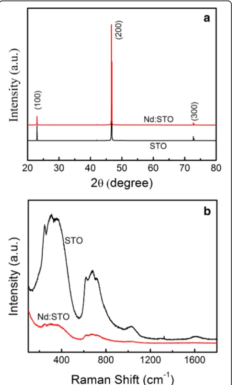
Figure 1a shows the XRD patterns of undoped STO and Nd:STO single crystals. All peaks are corresponding to the perovskite phase and can be indexed to the cubic space group Pm3m with lattice constant a≈3.905 Å. The peaks do not show any observable change after Nd implantation, indicating that the Nd doping has little effect on the bulk structure. The Raman spectra of undoped STO and Nd:STO single crystals are given in Fig. 1b. The Raman spectra of undoped STO shows two distinct broad bands originating from second-order scat-tering, which are centered at 200–400 cm−1 and 600–
800 cm−1and belongs to ideal cubic perovskite structure. The position of these two bands is in agreement with the
published literature [27, 28]. The broaden line with de-creased second-order broad band in Nd:STO is also ob-served, indicating a weaker centrosymmetry as a result of local disorder induced by Nd doping. Comparing with the XRD patterns, the Raman results indicate that there exist some structural defects on the surface of Nd:STO single crystal, which should be induced by the Nd doping.
It is generally known that the undoped STO single crystal is an insulating material. To investigate the Nd-doping impact on the electrical properties of STO single crystal, Hall effect was measured. The Hall results shows that the Nd:STO single crystal is at n-type conductivity, and the carrier concentration is about 2 × 1019 cm−1. This n-type conductivity can be attributed to the substi-tution of Nd3+into Sr2+sites.
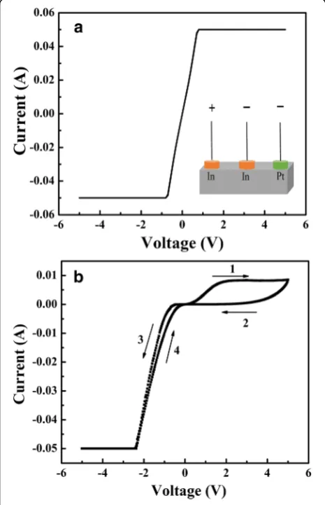
The inset of Fig. 2a shows the schematic illustration of In/ Nd:STO/In and Pt/Nd:STO/In devices. TheI–V characteris-tics of both In/Nd:STO/In and Pt/Nd:STO/In devices are plotted in Fig. 2a, b, respectively. The sweeping voltage was
applied as 0 V→5 V→0 V→−5 V→0 V with a 50-mA compliance current. The In/Nd:STO/In device has linearI– Vcurves (shown in Fig. 2a) and exhibits a good Ohmic con-tact between the pressed In electrodes and Nd:STO single crystal, but no RS effect appears, while the Pt/Nd:STO/In device shows reversible RS properties, as shown in Fig. 2b. When the applied voltage increases, the resistance transition occur, the direction of transition depends on the polarity of applied voltage. When the applied voltage decreases, the high- and low-resistance state (HRS and LRS) will be main-tained, indicating that the resistance state is stable and non-volatile after the formation. The largeI–Vhysteresis shows the Pt/Nd:STO/In device has the memory properties; the prototypical diode behavior indicates that a Schottky barrier is formed at the Pt and n-type Nd:STO interface and domi-nates the resistance of Pt/Nd:STO/In device. Therefore, it is easy to conclude that the RS effect of Pt/Nd:STO/In device comes from Schottky interface between Pt and Nd:STO sin-gle crystals. This result, RS is dependent on Schottky inter-face, is in agreement with our reported works on n-type Nb:STO single crystal [29].
To evaluate the potential for application of the Pt/ Nd:STO/In device in multi memory, the effect of the pulse width and amplitude on the resistance states was investigated and shown in Fig. 3a–c. The device was firstly set to LRS by a −5-V pulse with 100 ms width and then applied by a + 5-V pulse with varied pulse widths of 100 ns, 10μs, and 10 ms, respectively. The re-sistance was read at 0.1 V. The corresponding rere-sistance transition from LRS to intermediate resistance states or HRS was achieved, as shown in Fig. 3a. Figure 3b shows the consecutive RS cycles from HRS to LRS induced by the opposite polarity pulses. The results confirm that the multi-level resistance can be obtained by pulse voltage with different widths. The retention property of each re-sistance state was further investigated, and no significant change in resistance magnitudes was observed (shown in Additional file 1: Figure S1). Figure 3c presents typical non-volatile resistive memory loops controlled by pulses voltage. The Pt/Nd:STO/In device was firstly set to LRS by a pulse of−3 V, followed by sweeping the pulse volt-age to + 2 V (or + 3, + 4, and + 5 V) and back to−3 V with 100-ms pulse width. The resistance was read at 0.1 V. A series of intermediate resistance states can be achieved by adjusting the pulse magnitude. From the Fig. 3a–c, we have the result that multi-level resistance state of Pt/Nd:STO/In device can be achieved by adjust-ing the pulse width or magnitude, indicatadjust-ing that the device behaves as a memristor [23, 30].
It is generally known that photoexcitation of charge carriers occurs when the illuminated wavelength matches the optical bandgap of the active material. The generated electrons and holes will be separated by the internal electric field, which leads to the PV effect [23–25]. In the case of
[image:3.595.57.290.326.687.2]Pt/Nd:STO/In device, if the multi-level memory states are mainly determined by the depletion layer near the Pt/ Nd:STO interface, the PV effect is expected to be dependent on the memory states of the device. On the contrary, the PV is irrelevant to the memory states if the depletion layer is kept unchanged during the RS process. More interestingly, we found a memory-state-dependent PV effect for the Pt/Nd:STO/In device. Figure 4a, b shows
Fig. 3Consecutive RS cyclesafrom LRS to HRS andbfrom HRS to LRS. The device was firstly set to LRS (HRS) by a−5 V (+ 5 V) pulse with 100 ms width and then applied by a + 5 V (−5 V) pulse with varied pulse widths of 100 ns, 10μs, and 10 ms, respectively. The corresponding resistance transition from LRS (HRS) to intermediate resistance states or HRS (LRS).cR–Vhysteresis loops controlled by pulse voltage. The Pt/Nd:STO/In device was firstly set to LRS by a pulse of−3 V, followed by sweeping the pulse to + 2 V (or + 3, + 4, and + 5 V) and back to−3 V with 100-ms pulse width. All the resistance was read at 0.1 V
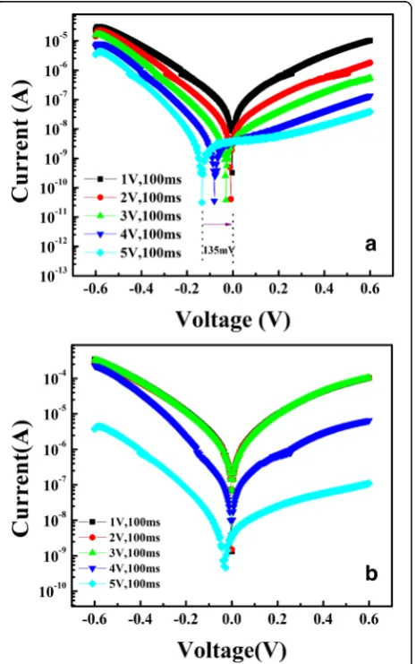
[image:4.595.59.294.92.669.2] [image:4.595.308.541.312.683.2]the I–Vcurves in the low-bias regime (−0.6 to + 0.6 V) after switching with a series of pulses from + 1 to + 5 V with 100 ms (switching from LRS to intermediate resistance states and to HRS) under the light illumination and dark, respectively. Under light illumination, the I–V curves of HRS exhibit notable shifts along the voltage axis, and the open-circuit voltage (Voc) (voltage at zero current) is as high as ~ 135 mV. Corresponding to a series of intermedi-ate resistance stintermedi-ates, the Voc gradually decreases with decreasing device resistance and is negligible small for LRS. Whereas little shift has been observed forI–Vcurves mea-sured in the dark. The similar result was obtained by Hu et al. [23]. Furthermore, a test method for Voc was reported by Shang et al. [24–26]. According to this method, the Voc was further measured at LRS and HRS. As expected, a voltage rise is produced by light illumination, and the Voc is dependence on the junction resistance (see Add-itional file 1: Figure S2). The above results testify that the magnitude of Voc depends on the memory states of Pt/Nd:STO/In device.
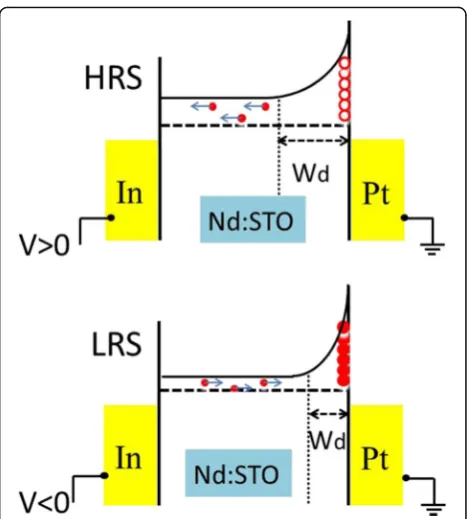
The multi-level memory and memory-state-dependent PV effect of Pt/Nd:STO/In device unambiguously suggest that the memory states are mainly determined by the depletion layer near the Pt/Nd:STO interface. In other words, the Schottky barrier width and height near the Pt/ Nd:STO interface will be modulated by sweeping voltage. According to the Raman results in Fig. 1b, there exist some defects (e.g., oxygen vacancies) at the Nd:STO sur-face. When a negative voltage or pulse was applied to the device, the injected electrons from the In electrode were trapped by the defects at the Pt/Nd:STO interface. The trapped electrons lead to narrower and lower Schottky barrier, resulting in LRS. In contrast, during the coming positive bias sweeping, the trapped electrons are released because of the existence of the depletion region, resulting in HRS. Furthermore, the spatial distribution of defects should be uneven. Fermi pinning may be formed at the high density defect, so the HRS and LRS can be kept when the applied bias is removed. The depletion layer can be adjusted by the pulse width or magnitude, so multi-level memory states were observed. Figure 5 shows the sche-matic diagram for the process of the electron trapping or detrapping on the Pt/Nd:STO interface.
The memory-state-dependent PV effect is induced by different width and height of the Pt/Nd:STO interface barrier at different memory state. The HRS with wider depletion region results in more electron-hole pairs gen-erated in depletion region under light illumination. The photogenerated electrons is driven into the Nd:STO bulk by the strong upward band bending in the HRS, and the holes tunnel through the barrier, resulting in a higher Voc. Conversely, the LRS with lower and narrower de-pletion region results in a lower Voc. In general, the Voc is dependent on interface barrier width and height which
is corresponding to the multi-level memory states of Pt/ Nd:STO/In device.
Note that both the memory states and the PV effect ex-hibit similar dependence on the switching bias, indicating the shared mechanism related to the electron depletion/ accumulation on the Nd:STO interface, revealing the importance of the interface barrier and interface charge redistribution (Fig. 5). The PV effect is induced by the photogenerated electrons and holes separated by the in-ternal electric field. So, the memory-state-dependent PV effect observed in Pt/Nd:STO/In device testify the RS is induced by the bias-induced modulation of Schottky bar-rier on Pt/Nd:STO interface and not by the formation of conductive filaments. The Voc is dependent on the mem-ory states, so such a resistance-state-dependent PV effect provides a new route by using Voc for sensing the mem-ory states of RS device in addition to the conventional resistance reading [23]. This new reading route is non-destructive and reliable because light illumination will not change the memory state of the devices.
Conclusions
In summary, we have investigated the RS and PV character-istics of single crystalline Nd:STO-based memristive de-vices. The RS effect is related to the Schottky junction near the interface of Pt and n-type Nd:STO single crystal. The memory states can be modulated by the pulse width or
[image:5.595.305.539.85.345.2]magnitude. The memory-state-dependent PV effect of the Pt/Nd:STO/In device is obtained by the switching voltage. These complimentary effects are attributed to the bias-induced modulation of the interface barrier, both in height and width, at the Pt/Nd:STO interface, which is caused by carrier injection and trapping/detrapping process on the Pt/Nd:STO interface. The results establish a strong connec-tion between the RS/PV effects and the modulaconnec-tion of the Nd:STO interface triggered by applied electric field and provide a new route by using Voc for non-destructively sensing multiple non-volatile memory states.
Additional file
Additional file 1:Supporting information. (DOCX 154 kb)
Abbreviations
HRS:High-resistance state;I–V: Current-voltage; LRS: Low-resistance state; PV: Photovoltage; RRAM: Resistance random access memories; RS: Resistance switching; XRD: X-ray diffraction
Funding
This work has been supported by the National Natural Science Foundation of China (grant no. 11404093), the Foundation of Henan Provincial Science and Technology Department (grant no. 132102210258), research funding from Henan Province (grant nos. 15A140001, 2015GGJS-021, and 17HAS-TIT014), and Henan University Emerging Cross and Characteristic Discipline Cultivation Program (grant no. xxjc20140016).
Authors’Contributions
XWS and SKW designed the whole experiment. GHL carried out the XRD and Raman measurement. SKW and XWS carried out the sample preparation, Hall andI–Vmeasurement, and analysis. GQL and CHJ participated in the discussion. XWS and WFZ supervised the whole study. All authors read and approved the final manuscript.
Competing Interests
The authors declare that they have no competing interests.
Publisher’s Note
Springer Nature remains neutral with regard to jurisdictional claims in published maps and institutional affiliations.
Received: 6 September 2017 Accepted: 2 January 2018
References
1. Souza RAD, Fleig J, Merkle R, Maier J (2003) SrTiO3: a model electroceramic.
Z Metallkunde 94:218
2. Zhang C, Liu Z, Chen Z, Xie Y, He R, Tang S, He J, Li W, Jia T, Rebec SN, Ma EY, Yan H, Hashimoto M, Lu D, Mo S-K, Hikita Y, Moore RG, Hwang HY, Lee D, Shen Z (2017) Ubiquitous strong electron-phonon coupling at the interface of FeSe/SrTiO3. Nat Commun 8:14468
3. Astala R, Bristowe PD (2002) A computational study of twist boundary structures in strontium titanate. J Phys Condens Matter 14:13635 4. Nili H, Ahmed T, Walia S, Ramanathan R, Kandjani AE, Rubanov S, Kim J,
Kavehei O, Bansal V, Bhaskaran M, Sriram S (2016) Microstructure and dynamics of vacancy-induced nanofilamentary switching network in donor doped SrTiO3−x memristors Nanotechnology 27:505210
5. Waser R, Dittmann R, Staikov G, Szot K (2009) Redox-based resistive switching memories––nanoionic mechanisms, prospects, and challenges. Adv Mater 21:2632
6. Wan T, Qu B, Du H, Lin X, Guan P, Lin Q, Chen N, Tan TT, Hang T, Chu D (2017) Tunable resistance switching in solution processed chromium-doped strontium titanate nanoparticles films. J Colloid Interf Sci 494:178
7. Andreasson BP, Janousch M, Staub U, Meijer GI, Ramar A, Krbanjevic J, Schaeublin R (2009) Origin of oxygen vacancies in resistive switching memory devices. J Phys Conf Ser 190:012074
8. Szot K, Speier W, Bihlmayer G, Waser R (2006) Switching the electrical resistance of individual dislocations in single-crystalline SrTiO3. Nat Mater 5:312
9. Janousch M, Meijer GI, Staub U, Delley B, Karg SF, Andreasson BP (2007) Role of oxygen vacancies in Cr-doped SrTiO3for resistance-change memory.
Adv Mater 19:2232
10. Wojtyniak M, Szot K, Wrzalik R, Rodenbucher C, Roth G, Wase R (2013) Electro-degradation and resistive switching of Fe-doped SrTiO3single
crystal. J Appl Phys 113:083713
11. Lenser C, Koehl A, Slipukhina I, Du H, Patt M, Feyer V, Schneider CM, Lezaic M, Waser R, Dittmann R (2015) Formation and movement of cationic defects during forming and resistive switching in SrTiO3thin film devices.
Adv Funct Mater 25:6360
12. Park J, Kwon DH, Park H, Jung CU, Kim M (2014) Role of oxygen vacancies in resistive switching in Pt/Nb-doped SrTiO3. Appl Phys Lett 105:183103
13. Mojarad SA, Goss JP, Kwa KSK, Zhou Z, Al-Hamadany RAS, Appleby DJR, Ponon NK, O’Neill A (2012) Leakage current asymmetry and resistive switching behavior of SrTiO3. Appl Phys Lett 101:173507
14. Wang Y, Shi X, Zhao K, Xie G, Huang S, Zhang L (2016) Controllable resistive switching in Au/Nb:SrTiO3microscopic Schottky junctions. Appl Sur Sci 364:718
15. Rodenbücher C, Speier W, Bihlmayer G, Breuer U, Waser R, Szot K (2013) Cluster-like resistive switching of SrTiO3:Nb surface layers. New J Phys 15:103017
16. Marchewka A, Cooper D, Lenser C, Menzel S, Du H, Dittmann R, Dunin-Borkowski RE, Waser R (2014) Determination of the electrostatic potential distribution in Pt/Fe:SrTiO3/Nb:SrTiO3thin-film structures by electron
holography. Sci Rep 4:6975
17. Yang M, Ren LZ, Wang YJ, FM Y, Meng M, Zhou WQ, SX W, Li SW (2014) Direct evidences of filamentary resistive switching in Pt/Nb-doped SrTiO3
junctions. J Appl Phys 115:134505
18. Wang YH, Zhao KH, Shi XL, Xie GL, Huang SY, Zhang LW (2013) Investigation of the resistance switching in Au/SrTiO3:Nb heterojunctions.
Appl Phys Lett 103:031601
19. Yang M, Ma X, Wang H, Xi H, Lv L, Zhang P, Xie Y, Gao H, Cao Y, Li S, Hao Y (2016) Evolution of resistive switching and its ionic models in Pt/Nb-doped SrTiO3junctions. Mater Res Express 3:075903
20. Nili H, Walia S, Kandjani AE, Ramanathan R, Gutruf P, Ahmed T, Balendhran S, Bansal V, Strukov DB, Kavehei O, Bhaskaran M, Sriram S (2015) Donor-induced performance tuning of amorphous SrTiO3memristive nanodevices:
multistate resistive switching and mechanical tunability. Adv Funct Mater 25:3172
21. Wang D, Ye J, Kako T, Kimura T (2006) Photophysical and photocatalytic properties of SrTiO3doped with Cr cations on different sites. J Phys Chem B
110:15824
22. Wang S, Ma ZZ, Xiong JJ, Li CJ, Hou YH (2016) Interface-enhanced sensitivity of photoconductivity to the electric current and magnetic field in La0.67Ca0.33MnO3/Nb-SrTiO3p-n junctions. Appl Phys Lett 109:251601
23. Hu W, Wang Z, Yu W, Wu T (2016) Optically controlled electroresistance and electrically controlled photovoltage in ferroelectric tunnel junctions. Nat Commun 7:10808
24. Shang DS, Sun JR, Shi L, Shen BG (2008) Photoresponse of the Schottky junction Au/SrTiO3:Nb in different resistive states. Appl Phys Lett 93:102106
25. Shang DS, Sun JR, Shi L, Wang ZH, Shen BG (2008) Resistance dependence of photovoltaic effect in Au/SrTiO3:Nb (0.5 wt%) Schottky junctions. Appl
Phys Lett 93:172119
26. Shang DS, Sun JR, Shen BG, Wuttig M (2013) Resistance switching in oxides with inhomogeneous conductivity. Chin Phys B 22:067202
27. Wu Q, Cen J, Goodman KR, White MG, Ramakrishnan G, Orlov A (2016) Understanding the interactions of CO2with doped and undoped SrTiO3.
ChemSusChem 9:1889
28. Rabuffetti FA, Kim HS, Enterkin JA, Wang Y, Lanier CH, Marks LD, Poeppelmeier KR, Stair PC (2008) Synthesis-dependent first-order Raman scattering in SrTiO3nanocubes at room temperature. Chem Mate 20:5628
29. Sun J, Jia CH, Li GQ, Zhang WF (2012) Control of normal and abnormal bipolar resistive switching by interface junction on In/Nb:SrTiO3interface.
Appl Phys Lett 101:133506