N A N O E X P R E S S
Open Access
Structural and optical properties of ITO/TiO
2
anti-reflective films for solar cell applications
Khuram Ali
*, Sohail A Khan and Mohd Zubir Mat Jafri
Abstract
Indium tin oxide (ITO) and titanium dioxide (TiO2) anti-reflective coatings (ARCs) were deposited on a (100) P-type monocrystalline Si substrate by a radio-frequency (RF) magnetron sputtering. Polycrystalline ITO and anatase TiO2 films were obtained at room temperature (RT). The thickness of ITO (60 to 64 nm) and TiO2(55 to 60 nm) films was optimized, considering the optical response in the 400- to 1,000-nm wavelength range. The deposited films were characterized by X-ray diffraction (XRD), Raman spectroscopy, field emission scanning electron microscopy (FESEM), energy dispersive spectroscopy (EDS), and atomic force microscopy (AFM). The XRD analysis showed preferential orientation along (211) and (222) for ITO and (200) and (211) for TiO2films. The XRD analysis showed that crystalline ITO/TiO2films could be formed at RT. The crystallite strain measurements showed compressive strain for ITO and TiO2films. The measured average optical reflectance was about 12% and 10% for the ITO and TiO2ARCs, respectively.
Keywords:ITO; TiO2; Sputtering; Antireflective films; Room temperature
Background
To deposit titanium dioxide (TiO2) and indium tin oxide (ITO) films, several techniques have been used, including radio-frequency (RF) sputtering, chemical vapor depos-ition [1], sol–gel [2], spray deposition [3], and electron-beam evaporation [4]. Low-deposition temperatures are required because high temperatures can degrade a sub-strate material for solar cells and plastic devices [5]. RF sputtering is a sophisticated process with high deposition rate and good reproducibility [6]. Most of these tech-niques require a type of heat treatment (250°C to 650°C) for the substrates during or after the deposition [1,2,4], due to insufficient crystallization at RT. This phenomenon leads to poor optical and structural properties [7]. RT de-position is important for photovoltaic devices as the ther-mal treatments may change the intended compositional distribution and also introduce defects that act as recom-bination centers for charge carriers in the solar cell device. Many attempts have been made to deposit ITO and TiO2 thin films on silicon substrates by RF sputtering technique at RT [8,9]. The ITO film exhibits excellent conductivity and it can be used as an ohmic contact on a p-type c-Si.
De Cesare, et al. achieved good electrical properties with ITO/c-Si contact at RT [10]. ITO has also become the at-tractive material for its anti-reflection (AR) properties and enhanced relative spectral response in the blue-visible re-gion. Optical device performance depends greatly on the surface morphology and crystalline quality of the semicon-ductor layer [11].
Another material, TiO2, is well known in silicon pro-cessing technology and has wide applications in optics and optoelectronics [12,13]. TiO2 films can be distinguished into three major polymorphs: anatase, rutile, and brookite. Each phase exhibits a different crystal configuration with unique electrical, optical, and physical properties. Anatase is the most photoactive but thermally instable and it con-verts into rutile phase above 600°C [14,15]. In this paper,
RF sputtering of ITO/TiO2 is used to eliminate the
standard high-temperature deposition process required for the formation of AR films. This also guarantees that the critical surface layer of the monocrystalline Si is not damaged. Present work reports the crystal structure, op-tical reflectance, and microstructure of the ITO/TiO2 AR films, RF sputter deposited on monocrystalline Si p-type (100) at RT.
* Correspondence:[email protected]
Nano-Optoelectronics Research and Technology Laboratory, School of Physics, Universiti Sains Malaysia, Penang 11800, Malaysia
Methods
ITO and TiO2were deposited on a 0.01- to 1.5-Ω cm
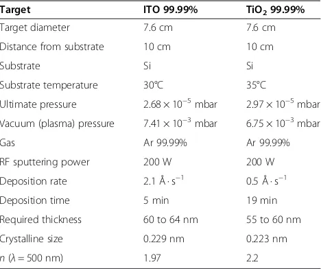
boron-doped monocrystalline Si wafer with one side polished. Silicon substrates were cleaned by a standard Radio Corporation of America method to remove sur-face contamination. After rinsing with deionized water (ρ> 18.2 MΩ cm) and N2 blowing, the ITO and TiO2 layers were deposited onto the front side of silicon wafers by RF sputtering using an Auto HHV500 sput-tering unit. Table 1 shows the sputsput-tering conditions for ITO and TiO2 films. The thickness of the
single-layer ITO and TiO2 films was deduced from the
fol-lowing relation:
d¼ λo
4n ð1Þ
of films and reference p-type (100) were measured using a Filmetrics F20 optical reflectometer using white light within the frequency range of 3 × 10¹⁴ to 7.5 × 10¹⁴ Hz. The combined wavelengths ranged from 400 to 1,000 nm with different colors. Raman studies were carried out using a spectroscopy system (Jobin Yvon HR 800 UV, Edison, NJ, USA).
Results and discussion
Typical XRD measurements of ITO films deposited by RF magnetron sputtering at RT are represented in Figure 1a. The low-intensity diffraction peak analogous to an incipi-ent crystallization of the ITO in the (222)-oriincipi-ented body-centered cubic (bcc) structure has been identified. While other diffraction peaks such as (400), (440), (611), and (622) showing crystallites with other orientation. The re-flection from the (2 2 2) crystalline plane resulted in a characteristic peak at 2θ= 30.81°, which was close to the peak (2θ= 30.581°) of the reference ITO [11,16,17]. The structural and morphological characteristics of the ITO film showed polycrystalline ITO growth on Si p-type (100) at RT [18].
Figure 1b shows the XRD patterns of the TiO2 film
grown on Si (100) substrates at RT. All diffraction peaks at 25.42°, 38.60°, 48.12°, and 55.39° corresponded to ana-tase (1 0 1), (1 1 2), (2 0 0), and (2 1 1) crystal planes, re-spectively [14,15]. The result of the XRD patterns also
Gas Ar 99.99% Ar 99.99%
RF sputtering power 200 W 200 W
Deposition rate 2.1 Å · s−1 0.5 Å · s−1
Deposition time 5 min 19 min
Required thickness 60 to 64 nm 55 to 60 nm
Crystalline size 0.229 nm 0.223 nm
[image:2.595.57.291.111.307.2]n(λ= 500 nm) 1.97 2.2
[image:2.595.57.540.555.720.2]showed that the anatase (2 0 0) is the preferential growth orientation while no rutile phases were observed. Anatase phase of TiO2 film grown on Si p-type (100) at RT is highly photoactive and have better AR properties as com-pared to other TiO2polymorphs: rutile and brookite [19]. XRD measurements affirm that nanocrystalline TiO2film with the anatase phase could be grown at RT without any apparent contamination. Table 1 lists the average crystallite size calculated using the Scherrer formula in Equation 2 [20].
D¼β0:9λ
cosθ ð2Þ
whereDis the average crystallite size,λis the X-ray ra-diation wavelength (0.15406 nm), β is the full width at
half maximum (FWHM) value, and θ is the diffraction
Bragg angle.
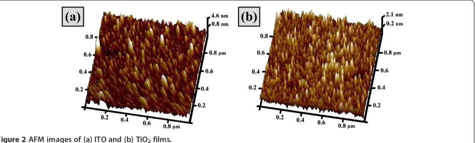
The film microstructure of ITO and TiO2 films was
also investigated by AFM, and the results are shown in Figure 2. Typical morphological features can be perceived
readily by visual inspection of Figure 2a,b. As can be seen, the granules of different scales exist in both the films and are scattered evenly in some ranges. In quantitative analyses on AFM images, surface morphology can be described by using the height roughness (Ra) and root mean square roughness (rms). Ra is described as the mean value of the surface height analogous to the cen-ter plane while rms is the standard deviation of the sur-face height within the given area [11]. From Figure 2a, height roughness (Ra) and root mean square roughness (rms) values of 0.75 and 9.4 nm, respectively, were de-termined for the surface roughness of ITO film depos-ited at RT. While from Figure 2b, Ra and rms values of 0.39 and 6.9 nm, respectively, were determined for the
surface roughness of TiO2 film deposited at RT. The
above analysis indicates that Ra and rms are strongly af-fected by the degree of accumulation and cluster size of the films.
[image:3.595.66.539.90.233.2]Cross-sectional view of ITO and TiO2films and respect-ive energy dispersrespect-ive X-ray (EDX) spectroscopy spectra are shown in Figure 3. FESEM cross-sectional view shows that the thickness of ITO and TiO2films was 59.5 and
[image:3.595.57.540.551.715.2]Figure 2AFM images of (a) ITO and (b) TiO2films.
60 nm, respectively, with an average ±0.5 nm uncer-tainty in thickness. FESEM front view of ITO and TiO2 films is shown in Figure 4. Visual inspection of front view represents that the granules of various scales were uniformly distributed in both ITO and TiO2films. These different scale granules influence the surface morphology of the films.
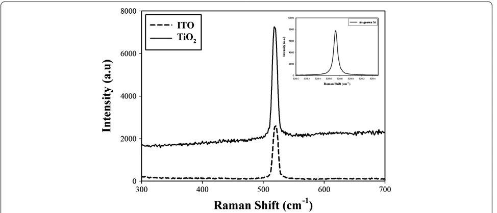
Figure 5 shows the Raman spectra of the ITO films, TiO2films, and as-grown Si sample based on the crystal-line silicon p-type (100) at RT. Raman spectroscopy explains the structural changes pertinent to the strain within the films. The Raman spectra of the as-grown Si sample showed a sharp solid line with an FWHM of only 0.08 cm−1located at 528.72 cm−1because of the scatter-ing of first-order phonons. The formation of the TiO2
[image:4.595.57.540.89.256.2]layer led to a peak shift at 519.52 cm−1with an FWHM of 10.24 cm−1, and to increased peak intensity compared with that of the ITO film and as-grown Si sample. The Raman spectra of the ITO layer shifted and sharpened at 518.81 cm−1with an FWHM of 9.76 cm−1, and led to an increased peak intensity compared with that of the as-grown Si sample. The preferential growth on Si was characterized by considerable shifting in the peak pos-ition. These UV peaks were due to the near band edge emission and heterogeneous properties of both the films. The Raman spectra revealed blue shifts in both film peaks. It is known that the blue shift of the peak attributed to the residual compressive strain [21,22]. This result can be at-tributed to the quantum confinement of optical phonons in the electronic wave function of the Si nanocrystals.
[image:4.595.56.543.506.715.2]Figure 4FESEM images of front views of (a) ITO and (b) TiO2films.
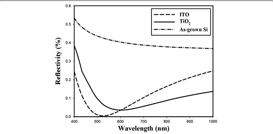
Figure 6 shows the measured reflectance spectra of
ITO and TiO2 layers with the as-grown Si sample on
non-textured Si substrates. The average solar reflectance of bare silicon was about 35%, whereas 10% and 12% were obtained by the deposition of TiO2 and ITO films, re-spectively, on the non-textured Si substrates. Reflection spectrum of ITO shows the minimum reflection of 0.4% at 523 nm while reflection spectrum of TiO2 shows the minimum reflection of 3.5% at 601 nm within the 400- to 1,000-nm range. It means the Si absorbance increased by
approximately 25% and 23% for ITO and TiO2 films,
respectively. The low reflectance enhances the absorption of the incident photons and hence increases the photo-generated current in Si solar cells. It reveals that the RT RF sputtering deposition of ITO and TiO2 films can be used as anti-reflective coatings (ARCs) for Si solar cells.
Conclusions
The work presents the structural and optical characteris-tics of ITO and TiO2ARCs deposited on a (100) P-type monocrystalline Si substrate by a RF magnetron sputter-ing at RT. X-ray diffraction proved the anatase TiO2and polycrystalline ITO films structure. Residual compres-sive strain was confirmed from the Raman analysis of the ITO and TiO2films which exhibited blue shifts in peaks at 518.81 and 519.52 cm−1excitation wavelengths, respectively.
FESEM micrographs showed that the granules of vari-ous scales are uniformly distributed in both ITO and TiO2films. Reflectance measurements of ITO and TiO2
films showed 25% and 23% improvement in the absorb-ance of incident light as compared to the as-grown Si. Low reflectivity value of 10% in the ITO film as compared to 12% of the TiO2film is attributed to the high rms value. Our results reveal that the highly absorbent polycrystalline ITO and photoactive anatase TiO2can be obtained by RF magnetron sputtering at room temperature. Both ITO and TiO2films can be used as ARCs in the fabrication of silicon solar cells.
Competing interests
The authors declare that they have no competing interests.
Authors’contributions
KA carried out the fabrication and characterization of the study and drafted the manuscript. SAK participated in its design and coordination and helped to draft the manuscript. MZMJ participated in the design and coordination of the study. All authors read and approved the final manuscript.
Acknowledgement
The authors acknowledge the Short Term Research Grant Scheme (1001/PFIZIK/845015) and Universiti Sains Malaysia (USM) for the Fellowship to Khuram Ali.
Received: 7 February 2014 Accepted: 3 April 2014 Published: 11 April 2014
References
1. Guo D, Ito A, Goto T, Tu R, Wang C, Shen Q, Zhang L:Effect of laser power on orientation and microstructure of TiO2films prepared by laser
chemical vapor deposition method.Mater Lett2013,93:179–182. 2. Sasani Ghamsari M, Bahramian AR:High transparent sol–gel derived
nanostructured TiO2thin film.Mater Lett2008,62:361–364.
3. Nguyen-Phan T-D, Pham VH, Cuong TV, Hahn SH, Kim EJ, Chung JS, Hur SH, Shin EW:Fabrication of TiO2nanostructured films by spray deposition
with high photocatalytic activity of methylene blue.Mater Lett2010,
[image:5.595.59.537.89.324.2]64:1387–1390.
8. Park J-O, Lee J-H, Kim J-J, Cho S-H, Cho YK:Crystallization of indium tin oxide thin films prepared by RF-magnetron sputtering without external heating.Thin Solid Films2005,474:127–132.
9. Guillén C, Herrero J:Comparison study of ITO thin films deposited by sputtering at room temperature onto polymer and glass substrates. Thin Solid Films2005,480–481:129–132.
10. De Cesare G, Caputo D, Tucci M:Electrical properties of ITO/crystalline-silicon contact at different deposition temperatures.IEEE Electron Device Let2012,
33:327–329.
11. Raoufi D, Kiasatpour A, Fallah HR, Rozatian ASH:Surface characterization and microstructure of ITO thin films at different annealing temperatures. Appl Surf Sci2007,253:9085–9090.
12. Vallejo B, Gonzalez-Mañas M, Martínez-López J, Morales F, Caballero MA:
Characterization of TiO2deposited on textured silicon wafers by
atmospheric pressure chemical vapour deposition.Sol Energ Mat Sol C
2005,86:299–308.
13. Ali K, Khan SA, Mat Jafri MZ:Enhancement of silicon solar cell efficiency by using back surface field in comparison of different antireflective coatings.Sol Ener2014,101:1–7.
14. Libardi J, Grigorov KG, Guerino M, da Silva Sobrinho AS, Maciel HS, Soares JP, Massi M:High quality TiO2deposited by reactive sputtering.
Structural and electrical peculiarities influenced by the specific experimental conditions.In Microelectronics Technology and Devices (SBMicro), 2013 Symposium on; 2-6 Sept2013,1:2013.
15. Zhang J-Y, Boyd IW, O'Sullivan BJ, Hurley PK, Kelly PV, Sénateur JP:
Nanocrystalline TiO2films studied by optical, XRD and FTIR
spectroscopy.J Non-Cryst Solids2002,303:134–138.
16. Kim H, Horwitz JS, Kushto G, Pique A, Kafafi ZH, Gilmore CM, Chrisey DB:
Effect of film thickness on the properties of indium tin oxide thin films. J Appl Phys2000,88:6021–6025.
17. Ishida T, Kobayashi H, Nakato Y:Structures and properties of electron‐beam‐evaporated indium tin oxide films as studied by X‐ray photoelectron spectroscopy and work‐function measurements.J Appl Phys1993,73:4344–4350.
18. Lien S-Y:Characterization and optimization of ITO thin films for application in heterojunction silicon solar cells.Thin Solid Films2010,518:S10–S13. 19. Dai S, Wu Y, Sakai T, Du Z, Sakai H, Abe M:Preparation of highly crystalline
TiO2nanostructures by acid-assisted hydrothermal treatment of
hexagonal-structured nanocrystalline titania/cetyltrimethyammonium bromide nanoskeleton.Nanoscale Res Lett2010,5:1829–1835. 20. Cullity BD:Element of X-ray Diffraction.3rd edition. USA: Wesley Publishing
Company; 1967.
21. Yang Y, Zhang Q, Zhang B, Mi WB, Chen L, Li L, Zhao C, Diallo EM, Zhang XX:
The influence of metal interlayers on the structural and optical properties of nano-crystalline TiO2films.Appl Surf Sci2012,258:4532–4537.
22. Alhomoudi IA, Newaz G:Residual stresses and Raman shift relation in anatase TiO2thin film.Thin Solid Films2009,517:4372–4378.
doi:10.1186/1556-276X-9-175
Cite this article as:Aliet al.:Structural and optical properties of ITO/TiO2
anti-reflective films for solar cell applications.Nanoscale Research Letters
20149:175.
Submit your manuscript to a
journal and benefi t from:
7 Convenient online submission
7 Rigorous peer review
7 Immediate publication on acceptance
7 Open access: articles freely available online
7 High visibility within the fi eld
7 Retaining the copyright to your article