N A N O E X P R E S S
Open Access
Characterization and density control of GaN
nanodots on Si (111) by droplet epitaxy using
plasma-assisted molecular beam epitaxy
Ing-Song Yu
1*, Chun-Pu Chang
2, Chung-Pei Yang
2, Chun-Ting Lin
2, Yuan-Ron Ma
3and Chun-Chi Chen
4Abstract
In this report, self-organized GaN nanodots have been grown on Si (111) by droplet epitaxy method, and their density can be controlled from 1.1 × 10¹⁰to 1.1 × 1011cm−2by various growth parameters, such as substrate temperatures for Ga droplet formation, the pre-nitridation treatment of Si substrate, the nitridation duration for GaN crystallization, andin situannealing after GaN formation. Based on the characterization ofin situRHEED, we can observe the surface condition of Si and the formation of GaN nanodots on Si. The surface nitridaiton treatment at 600°C provides a-SiNx layer which makes higher density of GaN nanodots. Crystal GaN nanodots can be observed by the HRTEM. The surface composition of GaN nanodots can be analyzed by SPEM andμ-XPS with a synchrotron x-ray source. We can find GaN nanodots form by droplet epitaxy and thenin situannealing make higher-degree nitridation of GaN nanodots.
Keywords:Molecular beam epitaxy; Gallium nitride; Quantum dots; Scanning photoemission microscopy; Reflection high-energy electron diffraction; Droplet epitaxy; Reflection high-energy electron diffraction; X-ray photoelectron spectroscopy
Background
Group-III nitride based semiconductors have been suc-cessful commercialized as light emitting diodes (LED) and high electron mobility transistors (HEMT) [1,2]. An enormous interest in gallium nitride (GaN) nanostruc-tures can be observed due to their strong carrier confine-ment phenomenon. GaN quantum dots (QDs) are highly potential materials for the applications in electronics such as single electron transistors, and in optoelectronics such as QD lasers, single photon source and photodetectors [3,4]. Recently, high-density GaN nanodots and nanorods are also expected to be illuminated working electrodes of photoelectrochemical water splitting to generate hydrogen gas. The hydrogen evolution by natural energy will be an important technique to prevent the global warming in the future [5].
For the fabrication of self-assembled semiconductor nanostructures, several methods were proposed so far.
For instance, molecular beam epitaxy (MBE) and metal organic chemical vapor deposition (MOCVD) provided nanodots growth via Stranski-Krastanov (SK) mode, which requires sufficient lattice mismatch between substrate, wetting layer and epi-layer [6-10]. However, there was still a challenge to have higher density, to easily control the growth, and to have fewer defects of self-organized semi-conductor nanostructures. In the last ten years, the drop-let epitaxy (DE) technique is another method to obtain nanostructures with some advantages over the SK mode. For example, a variety of quantum structures have been obtained by this technique such as dots, rings, holes, wires, dot pairs, dot disks, which can be fabricated on any sort of substrates. This flexible nanostructure-fabrication technique can apply to a wide range of materials by precisely controlling the lateral diffusion of metallic droplets and crystallization process [11,12]. Besides, many applications have been proposed by droplet epi-taxy technique: GaAs/AlGaAs quantum dot laser [13], single photon emitter on Si [14], and infrared photo-detector with strain-free GaAs quantum dot pairs [15].
* Correspondence:[email protected] 1
Department of Materials Science and Engineering, National Dong Hwa University, Hualien 97401, Taiwan
Full list of author information is available at the end of the article
For the growth of GaN nanodots by droplet epitaxy tech-nique, Ga droplets formation and then nitridation process for GaN crystallization, has been employed to fabricate GaN nanodots on c-plane sapphire, Si (111), 6H-SiC (0001) and Si3N4(0001)/Si(111). The size and density of
GaN nanodots were investigated by different Ga flux and substrate temperatures from the results of atomic force microscopy (AFM) [16-18]. For the first part of droplet epitaxy: Ga droplet formation, its growth mechanism has been experimentally and theoretically investigated in terms of nucleation, coalescence and ripening processes. Droplet number density can be easily controlled by a suitable choice of substrate temperature [19-21]. However, for the second part of droplet epitaxy: GaN crystallization, GaN nanodot formation was not a simple transformation of Ga droplets into GaN dots. Additional phenomena like surface diffusion of Ga and formation of a rough layer may play a role. Therefore, some further investigation is necessary to understand the growth mechanism of GaN nanodots by droplet epitaxy [22].
In this report, GaN nanodots were grown on Si (111) substrate by droplet epitaxy using plasma-assisted MBE system at various growth parameters. We focused on the characterization of GaN nanodots by scanning photo-emission microscopy (SPEM) and x-ray photoelectron spectroscopy (XPS) from a synchrotron radiation x-ray source.In situreflection high-energy electron diffraction (RHEED) was employed to observe Si surfaces and GaN nanodots. Ex situ transmission electron microscopy (TEM) was conducted to analyze the crystalline of GaN nanodots. In order to obtain higher density of GaN nanodots on Si for future applications, we also investi-gated the density of GaN nanodots by controlling the substrate temperatures, nitridation time for GaN crystallization, the pre-nitridation treatment of sub-strates, andin situannealing after GaN nanodot forma-tion from the images of field emission scanning electron microscopy (FESEM).
Methods
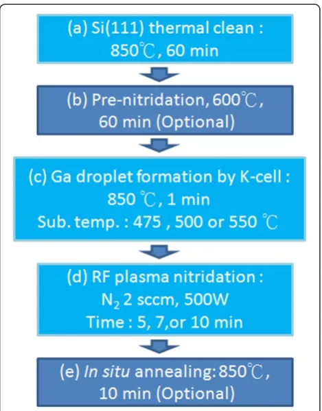
GaN nanodots by droplet epitaxy were carried out in our ULVAC MBE system with a radio frequency (RF) ni-trogen plasma source. The process flow and parameters of GaN nanodots formation is shown in Figure 1. Si (111) wafers were cleaned by acetone to remove organic impurity, cleaned by 10% HF solution to remove the na-tive oxide, and then put into MBE chamber immediately. Until the base pressure of chamber lower than 1.0 × 10⁻⁷Pa, thermal cleaning of Si substrates was conducted at 850°C for 60 min. Some of the samples had pre-nitridation treatment on Si substrates at temperature 600°C for 60 min. Then, Ga droplets were deposited by Ga Knudsen cell at 850°C for 1 min (beam equivalent pressure 1.9 × 10⁻⁴Pa) at substrate temperatures 475°C, 500°C and 550°C.
Nitridation process was followed to form GaN nanodots for 5 min, 7 min or 10 min. For the processes of Ga droplets nitridation and substrate pre-treatment, nitrogen plasma source operated at a RF forward power of 500 W and N2flux of 2 sccm, which provided beam
equivalent pressure 1.2 × 10⁻⁵Pa. After the formation of GaN nanodots, in situ annealing at 850°C for 10 min was the optional process for some samples.
[image:2.595.305.540.87.387.2]During the fabrication of each sample, surface quality and structure was monitored by in situ RHEED with electron beam energy 20 KeV. For the characterization of GaN nanodots, SPEM and μ-XPS were conducted on beamline U5 at the National Synchrotron Radiation Research Center (NSRRC) in Hsinchu, Taiwan, which can suffer photon energies from 60 to 1200 eV during high-resolution XPS measurement and provide photon beam size 90–100 nm in diameter [23]. The crystallinity of GaN nanodots was studied by high-resolution TEM, JEOL JEM-2010 F with accelerating voltage 200 KV. Ga droplets and GaN nanodots on Si were observed by a JEOL FESEM with accelerating voltage 15 KV, and their densities were obtained from SEM images.
Results and discussion In situ RHEED analysis
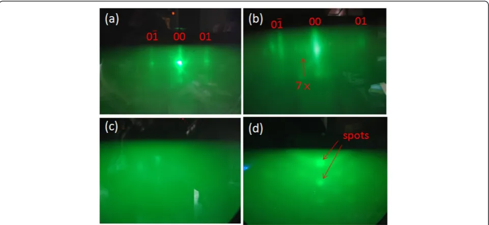
Figure 2(a) shows the in situ RHEED pattern of Si (111) before thermal cleaning, and a smooth surface gives long streaks in the RHEED pattern. After the thermal cleaning at 850°C for 60 min, Si (111)-7 × 7 reconstruction appears as shown in Figure 2(b). After the formation of Ga drop-lets on Si, RHEED pattern becomes cloudy as shown in Figure 2(c), which means a thin amorphous layer on Si. Followed by RF plasma nitridation, GaN nanodots formed on Si. Spotty and foggy RHEED pattern presents due to the rough surface by GaN nanodots on Si, shown in Figure 2(d). From the results of RHEED, we can find the pattern transition from 2D diffraction surface normal streaks to 3D diffraction Bragg spots during the growth of GaN nanodots by droplet epitaxy.
Some of the samples were prepared with pre-nitridation treatment at 600°C for 60 min in order to create different Si surface for the growth of GaN nanostructure. After the
pre-nitridation, entirely cloudy RHEED pattern is in appearance due to the amorphous nitride layer on Si. Low-temperature pre-nitridation on Si substrate can pro-duce an amorphous nitride layer for Ga deoplet formation. This result is different from the report by Gwo’s group. Single-crystal β-Si3N4 layer was formed by nitrogen
plasma nitridation at 830°C from their RHEED observa-tion [18]. After the growth of GaN nanodots on this sample, RHEED pattern gives rings centered as shown in Figure 3(b), which comes from the polycrystalline of GaN nanodots. From the results ofin situRHEED, we can not only observe the growth of GaN nanodots, but also deter-mine the surface condition which influences the growth and density of GaN nanodots (discuss latter).
Ex situ SEM and TEM analysis
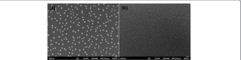
[image:3.595.58.539.89.310.2]Figure 4(a) is the SEM image of Ga droplets on Si. This sample was grown at substrate temperature 550°C by
Figure 2RHEED patterns. (a)Reflections of the Si (111) before thermal cleaning.(b)Si (111)-7 × 7 surface reconstruction after thermal cleaning. (c)Reflection of the Ga droplets on Si.(d)Reflection of crystal GaN nanodots on Si.
[image:3.595.57.539.594.705.2]K-cell 850°C for 1 min. The density of Ga droplets is 6.45 × 109 cm−2, and the average size is around 60 nm. For the same condition of Ga droplet formation, another sample formed GaN nanodots by RF plasma nitridation for 10 min as shown in Figure 4(b), their density be-comes 5.01 × 1010 cm−2, and the average size is around 15 nm. During the GaN crystallization, GaN nanodot formation was not a simple transformation of one Ga droplet into one GaN dot and their growth mechanism was more complex. To forward discussing their growth mechanism, the kinetics of Ga droplet formation was well studied: Ga droplets nucleate heterogeneously at the lower-energy sites on the surface or nucleate homo-geneously. Then, Ga droplets grow and coalesce [24,25]. After droplet formation, sample was immediately served nitrogen source by RF plasma, Ga atoms diffused on the surface quickly and reacted with limited nitrogen source to form GaN dots. It is the reason that one Ga droplet can form several GaN nanodots as the report in reference 22.
For the sample with the SEM image of Figure 4(b), high-resolution cross-sectional TEM was conducted to observe GaN nanodots. In Figure 5(a), GaN nanodots can be observed on Si, their size is around 10 nm. For the higher magnification of TEM image in the Figure 5(b), we can find the GaN nanodot crystal and a thin amorphous layer with thickness 1.5 nm between GaN nanodots and Si (111) substrate.
SPEM andμ-XPS analysis by synchrotron x-ray
[image:4.595.62.539.90.210.2]SPEM andμ-XPS were used to analyze the surface com-position of GaN nanodots on Si (111). For chemical state mapping of Ga-3d with block size 5μm × 5 μm, we got 16-channel SPEM images with binding energy from 14 eV to 26 eV. Because of the high density of GaN nanodots on Si (5.01 × 1010cm−2, see the SEM image of Figure 4(b)), the resolution of SPEM mapping did not good enough to clearly identify single GaN dot, so the result is not shown here. To control the density of GaN nanodots, we are going to discuss in the following section. The second mode of a SPEM system is photoelectron spectroscopy from a small spot area, so-calledμ-XPS. We conducted the measurements on 4 samples: Ga droplets (see SEM image of Figure 4(a)), GaN nanodots (see SEM image of Figure 4(b)), GaN nanodots with substrate pre-nitridation, GaN nanodots with pre-nitridation and an-nealing. Figure 6 shows Ga-3d XPS spectra for these 4 samples. The sample with Ga droplets has peak at 21 eV, which can be attributed to oxidized Ga due to exposure to air. As the GaN started to form by nitridation, the XPS peak of this sample shifts to the binding energy site of Ga-N, which corresponds to the formation of GaN. The sample with substrate pre-nitridation has similar XPS results with the one without nitridation. The pre-nitridation of Si substrate did not influence the chemical composition of GaN nanodots on Si. Furthermore, the
[image:4.595.60.539.588.704.2]Figure 4SEM images. (a)Ga droplets density 6.45 × 109 cm-2 and their size around 60 nm.(b)GaN nanodots density 5.01 × 1010 cm-2 and their size around 15 nm.
Ga-3d XPS peak shifts to 20 eV corresponding to the peak of GaN. We can find the annealing process in MBE made higher-degree nitridation of GaN nanodots.
Density analysis of GaN nanodots
In the end of this letter, we calculated the GaN nanodots density on Si from their SEM images to investigate the density control by different growth parameters. Firstly, Figure 7 shows GaN nanodots density as function of the substrate temperature and their SEM images. The lower substrate temperature we set during the Ga droplet formation, the higher density of GaN nanodots we get. For the sample grown at higher substrate temperature, the surface diffusion rate of Ga atoms is high. Ga ad-atoms re-evaporate and aggregate to form Ga droplet
more easily, which makes the Ga droplets lower density. For lower density Ga droplets on Si, we get lower density GaN nanodots after plasma nitridation. Secondly, we can also find the pre-nitridation treatment of Si substrate make higher density of GaN nanodots from the result of the two samples at substrate temperature 500°C in the blue cycle of Figure 7. From the results of RHEED in sec-tion In situ RHEED analysis, pre-nitridasec-tion process forms an amorphous nitride layer on the surface which provides nitrogen atoms for Ga nucleating heterogeneously. Nitri-dized surface might reduce the diffusion length of Ga ad-atoms. Therefore, the sample with substrate pre-nitridation has higher density of GaN nanodots.
Thirdly, we discuss GaN nanodots density as function of nitridation time as shown in Figure 8. The longer nitri-dation time we set, the higher GaN nanodots density we get. From the growth mechanism of GaN nanodots by droplet epitaxy, we know that one Ga droplet becomes several GaN nanodots during nitridation. Therefore, sufficient nitridation time provides more nitrogen source to form more GaN nanodots. Finally, in situ annealing process can also make the GaN nanodots density increase from the two samples of nitridation time 7 min shown in the blue cycle of Figure 8. As the result of XPS shows, in situ annealing not only makes higher degree of nitridation, but also forms higher density of GaN nanodots.
Conclusions
[image:5.595.57.292.90.258.2]In conclusion, we have demonstrated self-assembled and crystal GaN nanodots grown on Si (111) by droplet epitaxy using our PAMBE system. Their density can be controlled from 1.1 × 10¹⁰ to 1.1 × 1011 cm−2. The growth of GaN nanodots includes the Ga droplets nucleation, growth, coalescence, and GaN crystallization by plasma nitrogen source.In situRHEED, FESEM, HRTEM, SPEM and XPS
[image:5.595.303.539.529.686.2]Figure 6Ga-3d XPS core-level spectra for four samples.Ga droplets on Si (blue line), GaN nanodots on Si (pink line), GaN nanodots on Si with substrate pre-nitridation (black line), and GaN nanodots on Si with substrate pre-nitridation and in situ annealing (red line). The Ga-3d XPS peaks shift from 21 eV to 20 eV, which means the formation of GaN nanodots.
[image:5.595.56.293.533.685.2]Figure 7Density of GaN nanodots as function of substrate temperatures at 475°C, 500°C and 550°C and their SEM images. Density of GaN nanodots for two samples (in the blue cycle) with and without pre-nitridation treatment of substrate.
were employed to investigate the formation of GaN nano-dots. Through the understanding of their growth mechan-ism, density of GaN nanodots can be controlled by the parameters: substrate temperature of Ga droplet formation, pre-nitridation of Si substrate, nitridation time for GaN crystallization, and in situ annealing after GaN nanodot formation.
Abbreviations
LED:Light emitting diode; HEMT: High electron mobility transistor; GaN: Gallium nitride; QD: Quantum dot; MBE: Molecular beam epitaxy; MOCVD: Metal organic chemical vapor deposition; SPEM: Scanning photoemission microscopy; XPS: X-ray photoelectron spectroscopy; RHEED: Reflection high-energy electron diffraction; TEM: Transmission electron microscopy; FESEM: Field emission scanning electron microscopy.
Competing interests
The authors declare that they have no competing interests.
Authors' contributions
ISY carried out the design of the study and drafted the manuscript. CPC and CPY carried out all the experimental work. CTL participated in the design of the study. YRM performed the measurement of SPEM and XPS. CCC carried out the experiment of TEM. All authors read and approved the final manuscript.
Acknowledgements
The authors acknowledge Ministry of Science and Technology for financially supporting this study (MOST 103-2623-E-259-001-D and 103-2221-E-009 -033 -MY3), Chia-Hao Chen and Hung-Wei Shiu of NSRRC for the SPEM and XPS measurements, and Micheal Chen and Stanley Wu of ULVAC Taiwan for the maintenance of MBE system.
Author details
1Department of Materials Science and Engineering, National Dong Hwa University, Hualien 97401, Taiwan.2Institute of Photonic System, National Chiao Tung University, Tainan 71150, Taiwan.3Department of Physics, National Dong Hwa University, Hualien 97401, Taiwan.4National Nano Device Laboratories, Hsinchu 30078, Taiwan.
Received: 2 October 2014 Accepted: 12 December 2014 Published: 17 December 2014
References
1. Nakamura S, Pearton S, Fasol G:The Blue Laser Diode, The Complete Story.
2nd edition. Springer; 2000:3–5.
2. Su M, Chen C, Rajan S:Prospects for the application of GaN power devices in hybrid electric vehicle drive systems.Semicond ScI Technol
2013,28:074012.
3. Chow WW, Schneider HC:Theory of laser gain in InGaN quantum dots. Appl Phys2002,81:2566.
4. Ji LW, Su YK, Chang SJ, Liu SH, Wang CK, Tsai ST, Fang TH, Wu LW, Xue QK:
InGaN quantum dot photodetectors.Solid State Electron2003,47:1753. 5. Fujii K, Kato T, Sato K, Im I, Chang J, Yao T:Photoelectrochemical
application of GaN nanostructures on Si for hydrogen generation by water reduction.Phys Stat Solidi C2010,7:2218–2220.
6. Shen CH, Lin HW, Lee HM, Wu CL, Hsu JT, Gwo S:Self-assembled InN quantum dots grown on AlN/Si(111) and GaN/Al2O3(0001) by plasma-assisted molecular-beam epitaxy under stranski-krastanow mode thin solid films.Thin Solid Films2006,494:79–83.
7. Brown J, Wu F, Petroff PM, Speck JS:GaN quantum dot density control by rf-plasma molecular beam epitaxy.Appl Phys Lett2004,84:690–692. 8. Mashanov VI, Ulyanov VV, Timofeev VA, Nikiforov AI, Pchelyakov OP, Yu IS,
Cheng HH:Formation of Ge-Sn nanodots on Si(100) surfaces by molecular beam epitaxy.Nanoscale Res Lett2011,6:85.
9. Miyamura M, Tachibana K, Someya T, Arakawa Y:Stranski–Krastanow growth of GaN quantum dots by metalorganic chemical vapor deposition.J Cryst Growth2002,237–239:1316–1319.
10. Zhang J, Li S, Xiong H, Tian W, Li Y, Fang Y, Wu Z, Dai J, Xu J, Li X, Chen C:
Fabrication of low-density GaN/AlN quantum dots via GaN thermal decomposition in MOCVD.Nanoscale Res Lett2014,9:341.
11. Wu J, Hirono Y, Li X, Wang ZM, Lee J, Benamara M, Luo S, Mazur Y, Kim ES, Salamo GJ:Self-assembly of multiple stacked nanorings by vertically correlated droplet epitaxy.Adv Funct Mater2014,24:530–535. 12. Fuster D, Gonzalez Y, Gonzalez L:Fundamental role of arsenic flux in
nanohole formation by Ga droplet etching on GaAs(001).Nanoscale Res Lett2014,9:309.
13. Mano T, Kuroda T, Mitsuishi K, Nakayama Y, Noda T, Sakoda K:GaAs/AlGaAs quantum dot laser fabricated on GaAs (311)Asubstrate by droplet epitaxy.Appl Phys Lett2008,93:203110.
14. Cavigli L, Bietti S, Accanto N, Minari S, Abbarchi M, Isella G, Frigeri C:High temperature single photon emitter monolithically intergrated on silicon. Appl Phys Lett2012,100:231112.
15. Wu J, Shao D, Dorogan VG, Li AZ, Li S, DeCuir EA Jr, Manasreh MO, Wang ZM, Mazur YI, Salamo GJ:Intersublevel infrared photodetector with strain-free GaAs quantum dot pairs grown by high temperature droplet epitaxy.Nano Lett2010,10:1512–1516.
16. Wang Y, Ozcan AS, Sanborn C, Ludwig KF, Bhattacharyya A, Chandrasekran R, Moustakas TD, Zhou L, Smith DJ:Real-time x-ray studies of gallium nitride nanodot formation by droplet heteroepitaxy.J Appl Phys2007,
102:073522.
17. Kondo T, Saitoh K, Yamamoto Y, Maruyama T, Naritsuka S:Fabrication of GaN dot structures on Si substrates by droplet epitaxy.Phys Sta Sol A
2006,203:1700–1703.
18. Wu CL, Chou LJ, Gwo S:Size- and shape-controlled GaN nanocrystals grown on Si(111) substrate by reactive epitaxy.Appl Phys Lett2004,
85:2071–2073.
19. Madras G, McCoy BJ:Temperature effects on the transition from nucleation and growth to Ostwald ripening.Chem Eng Sci2004,59:2753– 2765.
20. Li C, Zeng ZQ, Fan DS, Hirono Y, Wu J, Morgan TA, Hu X, Yu SQ, Wang ZM, Salamo GJ:Bismuth nano-droplets for group-V based molecular-beam droplet epitaxy.Appl Phys Lett2011,99:243113.
21. Somaschini C, Bietti S, Trampert A, Jahn U, Hauswald C, Riechert H, Sanguinetti S, Geelhaar L:Control over the number density and diameter of GaAs nanowires on Si(111) mediated by droplet epitaxy.Nano Lett
2013,13:3607–3613.
22. Debnath RK, Stoica T, Besmehn A, Jeganathan K, Sutter E, Meijers R, Luth H, Calarco R:Formation of GaN nandots on Si(111) by droplet nitridation. J Cryst Growth2009,311:3389–3394.
23. Chen CH, Wang SC, Yeh CM, Hwang J, Klauser R:A scanning
photoelectron microscopy study of AlN/SixNy insulating stripes.Surf Sci
2005,599:107.
24. Family F, Meakin P:Kinetics of droplet growth-processes–simulations, theory, and experiments.Phys Rev A1989,40:3836.
25. Naritsukaa BS, Kondoa T, Otsuboa H, Saitoha K, Yamamotob Y, Maruyama T:
In situ annealing of GaN dot structures grown by droplet epitaxy on (111) Si substrates.J Cryst Growth2007,300:118–122.
doi:10.1186/1556-276X-9-682
Cite this article as:Yuet al.:Characterization and density control of GaN nanodots on Si (111) by droplet epitaxy using plasma-assisted molecular beam epitaxy.Nanoscale Research Letters20149:682.
Submit your manuscript to a
journal and benefi t from:
7Convenient online submission
7Rigorous peer review
7Immediate publication on acceptance
7Open access: articles freely available online
7High visibility within the fi eld
7Retaining the copyright to your article