N A N O E X P R E S S
Open Access
Synthesis of gallium nitride nanostructures by
nitridation of electrochemically deposited gallium
oxide on silicon substrate
Norizzawati Mohd Ghazali
1, Kanji Yasui
2and Abdul Manaf Hashim
1*Abstract
Gallium nitride (GaN) nanostructures were successfully synthesized by the nitridation of the electrochemically deposited gallium oxide (Ga2O3) through the utilization of a so-called ammoniating process. Ga2O3nanostructures were firstly deposited on Si substrate by a simple two-terminal electrochemical technique at a constant current density of 0.15 A/cm2using a mixture of Ga2O3, HCl, NH4OH and H2O for 2 h. Then, the deposited Ga2O3sample was ammoniated in a horizontal quartz tube single zone furnace at various ammoniating times and temperatures. The complete nitridation of Ga2O3nanostructures at temperatures of 850°C and below was not observed even the ammoniating time was kept up to 45 min. After the ammoniating process at temperature of 900°C for 15 min, several prominent diffraction peaks correspond to hexagonal GaN (h-GaN) planes were detected, while no diffraction peak of Ga2O3structure was detected, suggesting a complete transformation of Ga2O3to GaN. Thus, temperature seems to be a key parameter in a nitridation process where the deoxidization rate of Ga2O3to generate gaseous Ga2O increase with temperature. The growth mechanism for the transformation of Ga2O3to GaN was proposed and discussed. It was found that a complete transformation can not be realized without a complete deoxidization of Ga2O3. A significant change of morphological structures takes place after a complete transformation of Ga2O3to GaN where the original nanorod structures of Ga2O3 diminish, and a new nanowire-like GaN structures appear. These results show that the presented method seems to be promising in producing high-quality h-GaN nanostructures on Si.
Keywords:Electrochemical deposition; Gallium oxide; Gallium nitride; Nanostructure; Nitridation
Background
Gallium nitride (GaN) is a very hard, chemically and mech-anically stable wide bandgap (3.4 eV) semiconductor mater-ial with high heat capacity and thermal conductivity which makes it suitable to be used for sensors [1-8], high power electronic devices such as field-effect transistor (FET) [9] and optoelectronic devices such as light-emitting diode (LED) [10]. Up to this date, many techniques have been explored to synthesize GaN nanostructures including nano-wires, nanorods, nanodots and so forth since such low-dimensional nanostructures are promising for increasing the performance optoelectronic devices and the sensitivity of sensors [11,12].For example, GaN nanorods and nano-wires have been applied for chemical sensing application as
reported by Wright et al. [13] and Huang Y et al. [14], respectively, due to a large surface to volume ratio. GaN nanodots have been used in photodetectors as reported by Kumar et al.[15].
Recently, GaN on silicon carbide (SiC) or sapphire sub-strate have been widely used for several specific electronic applications. However, these substrates are expensive and not available in large wafer size [16]. According to Kukushkin et al., Si substrate seems to be more preferable for the heterostructure growth of GaN due to the availa-bility of Si in large wafer size, the low price of Si and the maturity of Si-based technology [17]. In addition, the inte-gration of GaN-based devices on Si platform seems to be very attractive for the hybrid integration towards ‘More than Moore’ technology [18]. Several vapor-phase tech-niques have been reported for growing GaN nanostructures directly on Si with high quality which include molecular beam epitaxy (MBE) [19], metal-organic chemical vapor * Correspondence:[email protected]
1
Malaysia-Japan International Institute of Technology, Universiti Teknologi Malaysia, Jalan Semarak, 54100 Kuala Lumpur, Malaysia
Full list of author information is available at the end of the article
deposition (MOCVD) [20] and hydride vapor phase epitaxy (HVPE) [21]. However, these vapor-phase techniques are too expensive and their growth parameters are quite com-plicated. In recent years, a transformation of the grown gal-lium oxide (Ga2O3) structures on Si to GaN by a so-called
nitridation seems to be a simple method to create a GaN/ Si heterostructure [22]. Here, a nitridation is achieved by annealing the Ga2O3structures in ammonia gas. Li et al.
reported the repeatable transformation of the CVD-grown GaN structures to Ga2O3structures by an annealing in air
and back to GaN structures by an annealing in ammonia [23]. Moreover, there are several studies reporting the formation of GaN nanostructures by annealing the sput-tered Ga2O3layer on metal-coated Si substrates in
ammo-nia [24-27]. To our knowledge, the nitridation of the electrochemically deposited Ga2O3 structures on bare Si
substrates to form GaN nanostructures without the assist-ance of metal catalyzers does not appear in the published literature.
Recently, we report the growth of Ga2O3nanostructures
directly on Si without any assistance of metal catalyzer by using a simple electrochemical deposition [28]. This liquid-phase technique provides several advantages such as high controllability of thickness and morphologies of Ga2O3
nanostructures due to a less number of growth parameters. In this work, we investigate the formation of GaN nano-structures by ammoniating the electrochemically deposited
β-Ga2O3 nanostructures on Si substrate. Up to this date,
no such similar work is reported where a combination of liquid-phase and vapor-phase methods is utilized to form a GaN/Si heterostructure. The effects of the ammoniating times and temperatures were studied. The mechanism for the growth of GaN was proposed and discussed.
Methods
In this study, the synthesis can be divided into two major processes; i) a formation of Ga2O3 structures as
the ‘seed’structures and ii) an ammoniating process to transform Ga2O3 to be GaN. The deposition of Ga2O3
on Si (100) substrate (resistivity of 15 to 25Ω· cm) was carried out by a simple two-terminal electrochemical process. In the electrochemical process, a mixture of Ga2O3(99.99%), HCl (36%), NH4OH (25%) and DI water
was used as an electrolyte [28]. Since Ga2O3is insoluble
in water, HCl is added to dissolve Ga2O3. The
prepar-ation of electrolyte was done as follows. First, Ga2O3
was dissolved in 1.5 ml HCl. Then, 6.5 ml DI water was added into the solution, followed by NH4OH as a
pre-cipitator, so that the pH of the mixture could be easily adjusted. The deposition was done in electrolyte with Ga2O3 molarity of 1.0 M (pH 6) at a constant current
density of 0.15 A/cm2. The Si substrate was cleaned with modified RCA cleaning using ethanol, acetone and DI water prior to the deposition in order to remove a native
oxide layer. The growth time was fixed at 2 h. In this electrochemical process, a platinum (Pt) wire was used as an anode and Si substrate as a cathode. The sche-matic of electrochemical setup is shown in Figure 1a. After the deposition, the sample was immersed into the DI water to remove any unwanted residue.
The electrochemically deposited Ga2O3 was
ammoni-ated in a quartz tube furnace as shown in Figure 1b, at various times of 15, 30 and 45 min and temperatures of 800°C, 850°C and 900°C under a flow of ammonia (NH3)
gas of 100 sccm at atmospheric pressure. The timing chart of ammoniating process is shown in Figure 1c. Be-fore starting the ammoniating process, the sample was put inside the quartz tube furnace and then the nitrogen (N2) gas was purged for 10 min to flush out the air in
the quartz tube. After that, the temperature was in-creased up to the setting temperatures, i.e. 800°C, 850°C and 900°C from room temperature (RT) with a ramping rate of 28°C/min. After reaching the setting temperature, N2 gas was stopped and NH3 gas was introduced into
the furnace. The furnace was immediately switched off upon reaching the setting ammoniating time. At the same time, NH3 gas was immediately stopped and N2
gas was purged back into the furnace for 1 h to remove the remaining NH3gas during the cooling down process.
The ammoniated structures were characterized using field-emission scanning electron microscopy (FESEM; Hitachi SU8083, Hitachi, Ltd, Chiyoda-ku, Japan), energy disper-sive X-ray (EDX) spectroscopy and X-ray diffraction (XRD; Bruker D8 Advance, Bruker AXS, Inc., Yokohama-shi, Japan).
Results and discussion
The nitridation of Ga2O3to form GaN can be described
as follows. Firstly, NH3decomposes to N2and H2at high
temperatures as illustrated by Equation 1 [29]. Then, Ga2O3 structures are deoxidized by H2to form gaseous
Ga2O as illustrated by Equation 2. Finally, GaN structure
is synthesized through the reaction of Ga2O and NH3.
2NH3ð Þg→N2ð Þ þg 3H2ð Þg ð1Þ
Ga2O3ð Þ þs 2H2ð Þg →Ga2O gð Þ þ2H2O gð Þ ð2Þ
Ga2O gð Þ þ2NH3ð Þg →2GaN sð Þ þ2H2ð Þ þg H2O gð Þ
ð3Þ
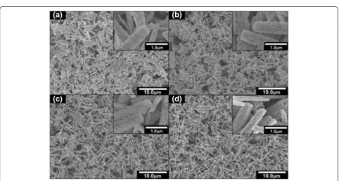
Figure 2a shows the top view FESEM images of the electrochemically deposited Ga2O3nanorods on Si
sub-strate before the ammoniating process was applied. The lengths and diameters of the grown Ga2O3 nanorods
Figure 1Schematic of (a) electrochemical setup, (b) nitridation set up and (c) growth timing chart.
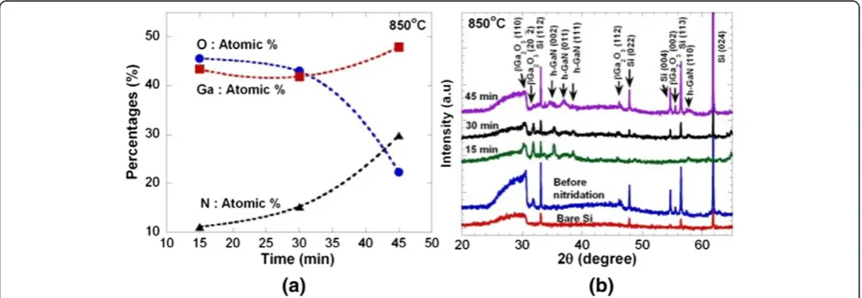
[image:3.595.57.540.460.717.2]Figure 2b,c,d shows the top view FESEM images after the ammoniating process at 850°C for 15, 30 and 45 min, respectively. In a glance, it can be seen that there is no significant change of morphology taking place even at long ammoniating time of 45 min. How-ever, it can be seen that there is a slight change on the surface of nanorods where the numbers of ‘hole’ in-crease with the ammoniating time. From the EDX ana-lysis as shown in Figure 3a, the atomic percentage of N increases with ammoniating time while the atomic per-centage of O decreases and the drastic changes seem to take place after ammoniating time of 30 min. Figure 3b shows the XRD spectra of samples before and after the ammoniating process at 850°C for 15, 30 and 45 min together with the XRD spectra of bare Si. In the bare Si, five peaks were observed at 33.1°, 47.8°, 54.7°, 56.4° and 61.8° corresponding to Si(112), Si(002), Si(004), Si(113) and Si(024), respectively. The as-grown Ga2O3nanorods
show three prominent peaks at 31.8°, 46.2° and 55.5° corresponding to β-Ga2O3(202), β-Ga2O3(112) and β
-Ga2O3(002), respectively. After being ammoniated for
15, 30 and 45 min, several peaks corresponding to hexagonal GaN (h-GaN) planes were observed. However,
β-Ga2O3-related peaks were still detected in all grown
samples suggesting that β-Ga2O3 structures are not
completely being transformed to GaN. From these XRD results, it can be said that an ammoniating time is not a dominant parameter since the complete transformation of Ga2O3to GaN does not occur even at a long
ammo-niating time of 45 min.
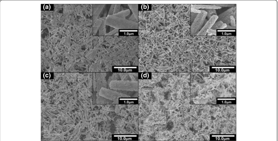
Figure 4a,b,c,d shows the FESEM images for the as-grown sample and the ammoniated samples at tempera-tures of 800°C, 850°C and 900°C for 15 min, respectively. It is noted here that β-Ga2O3 nanorods as shown in
Figure 4a were also grown using the similar procedures and conditions with the samples shown in Figure 2
where their properties are similar. After being ammoni-ated at 800°C and 850°C, the general shape of the nano-rods is still being preserved where no significant change in their morphologies is observed, as shown in Figure 4b,c, respectively. However, the same phenomenon with the samples shown in Figure 2 was observed where the num-bers of ‘hole’structures in the nanorods increase with the temperature. When the sample was further ammoniated at 900°C, as shown in Figure 4d, the structures have chan-ged from nanorods to nanowires with the estimated lengths of 0.4 to 1.0μm and diameters of 0.05 to 0.08μm. This result is consistent with the result reported by Kim et al. where they claimed that the change of morph-ology could be significantly affected by the ammoniating temperature [30]. Figure 5a shows the EDX analysis for the samples ammoniated at temperatures of 800°C, 850°C and 900°C. It can be seen that the atomic percentage of N increases with temperature while the atomic percentage of O decreases. As shown in Figure 5a, the drastic change in the atomic percentage seems to take place from 800°C to 850°C. Figure 5b shows the XRD spectra of the as-grown samples and the ammoniated samples at temperatures of 800°C, 850°C and 900°C for 15 min together with the XRD spectra of bare Si. After being ammoniated at 800°C, 850°C and 900°C, several h-GaN-related peaks were ob-served. However, as expected, β-Ga2O3-related peaks are
being detected for the samples ammoniated at 800°C and 850°C, suggesting the incomplete transformation of β -Ga2O3 to GaN. It can be simply said that the complete
transformation was achieved at ammoniating temperature of 900°C where no β-Ga2O3-related peak was observed
[image:4.595.57.540.538.705.2]except h-GaN peaks. The peaks related to GaN structures were detected at 32.5°, 34.6°, 36.9° and 58.0° corresponding to h-GaN(010), h-GaN(002), h-GaN(011) and h-GaN (110), respectively. The obtained results show a similar tendency with the results reported by Li et al. [31] where
Figure 3EDX analysis and XRD spectra. (a)Atomic percentage obtained from the EDX analysis and(b)XRD spectra of the samples nitridated at 850°C with various nitridation times.
the complete transformed GaN with hexagonal wurtzite structure was obtained at a temperature of 900°C. It is noted that from the EDX analysis, the atomic percentage of O is not zero in the sample of 900°C. It is speculated that the detected O element is contributed by a native oxide layer in the sample after being exposed to air ambi-ent. From these XRD results, it can be said that an ammo-niating temperature is the key parameter in producing the complete transformation of Ga2O3 to GaN since it takes
only a short ammoniating time of 15 min.
Based on the obtained morphological and structural properties, the reaction mechanism for the transformation
of Ga2O3 to GaN under a flow of ammonia with the
dependence of temperatures is proposed and discussed. In principle, as shown by Equation 1, with the increase of temperature, the decomposition rate of NH3should be
in-creased, resulting to the generation of a high density of H2.
Then, this leads to the higher deoxidization or vaporization rate of Ga2O3structures to form gaseous Ga2O, as
illus-trated by Equation 2 [32]. Finally, this situation would in-crease the reaction of gaseous Ga2O and NH3to promote
the formation of a GaN structure. This means that the transformation of Ga2O3to GaN does not proceed without
[image:5.595.57.540.90.335.2]the deoxidation or vaporization of Ga2O3 or, in other Figure 4Top view FESEM images of samples. (a)Before nitridation,(b)after nitridation at 800°C,(c)after nitridation at 850°C and(d)after nitridation at 900°C for 15 min.
[image:5.595.58.539.538.704.2]words, without the existence of gaseous Ga2O. Due to such
deoxidization and reaction activities, it is speculated that the original morphological structure of Ga2O3 will be
diminished and a new morphological structure of GaN will be formed. As shown in Figure 4b, the SEM image of the ammoniated structure at temperature of 800°C shows no significant change of the morphology as compared to the unammoniated structure shown in Figure 4a. This seems to show that the temperature of 800°C is considerably low for the aggressive deoxidization or vaporization of Ga2O3
to take place, resulting to low reaction of gaseous Ga2O
and NH3to form GaN. This also agrees with the XRD
ana-lysis as shown in Figure 5b where the sample ammoniated at temperature of 800°C contains a mixture of Ga2O3and
GaN structures. Figure 6a illustrates the growth mechan-ism for the temperature of 800°C. When the temperature is increased to 850°C, the morphology of the ammoniated structure shows a slight change where the numbers of ‘hole’structures seem to be increased as shown in Figure 4c. It can be said that the deoxidization or vaporization rate of Ga2O3slightly increases to form gaseous Ga2O. However,
since the original structure of Ga2O3 does not diminish
and the XRD spectra also shows a mixture of Ga2O3and
GaN, it can be said that the temperature of 850°C is still not favorable to drastically increase the density of gaseous Ga2O to continuously react with NH3 to form a GaN
structure. Figure 6b illustrates the growth mechanism for the temperature of 850°C. At high temperature of 900°C, as shown in Figure 4d, it can be seen that the original nanorod structure of Ga2O3 has diminished and a new
structure in the form of nanowire-like structure has been produced. It can be said that temperature of 900°C seems to be high enough to realize a complete deoxidization of Ga2O3to generate a high density of gaseous Ga2O. Thus,
the reaction of gaseous Ga2O and NH3seems to be well
promoted at such condition to form GaN nanowires. It is noteworthy that during the ammoniating process at temperature of 900°C, white‘cloudy’ambient was observed in the furnace which seems to indicate the aggressive deox-idization of Ga2O3to form Ga2O gaseous. After
[image:6.595.55.540.358.703.2]ammoni-ating process, it was found that the original white colour of the as-grown Ga2O3 diminished and new structures in
Figure 6Proposed growth mechanism for the transformation Ga2O3to GaN.At ammoniating temperatures of(a)800°C,(b)850°C and (c)900°C.
light yellow colour appeared. The XRD spectra as shown in Figure 5b reveals that the detected peaks belong only to the structures of GaN. It can be said that the temperature of 900°C is favorable to drastically increase the deoxidization rate of Ga2O3to generate gaseous Ga2O to continuously
react with NH3 to form GaN with new morphological
nanostructures.
Conclusions
The nitridation of the electrochemically grown Ga2O3
nanostructures to form GaN nanostructures on Si plat-form have been studied by varying the ammoniating times and temperatures. The complete transformation of Ga2O3
nanorods to h-GaN nanowires was achieved at 900°C with a short ammoniating time of 15 min. The obtained results suggest that the effect of the ammoniating temperature in realizing a complete transformation is more prominent than the ammoniating time. Form the proposed growth mechanism, it was found that a complete transformation to GaN nanostructures can not be realized without a complete deoxidization of Ga2O3. In a complete
trans-formation process, it seems to show the occurence of morphological change. The presented method seems to be promising for the formation of h-GaN nanostructures on Si for the applications in sensing and optoelectronics.
Competing interests
The authors declare that they have no competing interests.
Authors’contributions
NMG designed and performed the experiments, participated in the data analysis and prepared the manuscripts. KY participated in the nitridation process and revision of manuscript. AMH conceived the study, designed the experiments, participated in the data analysis and revised the manuscript. All authors read and approved the final manuscript.
Acknowledgements
The authors would like to thank for the supports provided by MIMOS Berhad and Universiti Sains Malaysia. N. M. Ghazali thanks Malaysia-Japan International Institute of Technology (MJIIT) for the scholarship. This work was supported by Nippon Sheet Glass Corp, Hitachi Foundation, MJIIT, universiti Teknologi Malaysia, Malaysian Ministry of Education and Malaysian Ministry of Science, Technology and Innovation through various research grants.
Author details
1
Malaysia-Japan International Institute of Technology, Universiti Teknologi Malaysia, Jalan Semarak, 54100 Kuala Lumpur, Malaysia.2Department of
Electrical Engineering, Nagaoka University of Technology, Kamitomioka-machi, Nagaoka, Niigata 940-2137, Japan.
Received: 24 October 2014 Accepted: 9 December 2014 Published: 18 December 2014
References
1. Abidin MSZ, Shahjahan, Hashim AM:Surface reaction of undoped AlGaN/ GaN HEMT based two terminal device in H+ and OH-ion-contained aqueous solution.Sains Malaysiana2013,2:197–203.
2. Abidin MSZ, Hashim AM, Sharifabad ME, Rahman SFA, Sadoh T:Open-gated pH sensor fabricated on an undoped-AlGaN/GaN HEMT structure.Sensors
2011,11:3067–3077.
3. Mohamad M, Mustafa F, Rahman SFA, Abidin MSZ, Ali NK, Hashim AM, Aziz AA, Hashim MR:The sensing performance of hydrogen gas sensor utilizing undoped-AlGaN/GaN HEMT.J Appl Sci2010,16:1797–1801.
4. Pearton SJ, Fan R:Gallium nitride-based gas, chemical and biomedical sensors.Instrum Meas Mag IEEE2012,15:16–21.
5. Chu BH, Sam Kang BS, Hung SC, Chen KH, Ren F, Sciullo A, Gila BP, Pearton SJ:Aluminum gallium nitride (GaN)/GaN high electron mobility transistor-based sensors for glucose detection in exhaled breath condensate.J Diabetes Sci Technol2010,4:171–179.
6. Chitara B, Late DJ, Krupanidhi SB, Rao CNR:Room-temperature gas sensors based on gallium nitride nanoparticles.Solid State Commun2010,
150:2053–2056.
7. Schalwig J, Muller G, Ambacher O, Stutzman M:Group III-nitride based gas sensing devices.Phys Stat Sol (a)2001,185:39–45.
8. Lee DS, Lee JH, Lee YH, Lee DD:GaN thin films as gas sensors.Sensor Actuat B Chem2003,6989:1–6.
9. Micovic M, Hashimoto P, Hu M, Milosavljevic I, Duvall J, Willadesen PJ, Wong WS, Conway AM, Kurdoghlian A, Deelman PW, Moon JS, Schmitz A, Delaney MJ:
GaN double heterojunction field effect transistor for microwave and millimeterwave power applications.IEDM Technical Digest2004,33:807–810. 10. Choi JH, Zoulkarneev A, Kim S, Baik CW, Yang MH, Park SS, Suh H, Kim UJ,
Son HB, Lee JS, Kim M, Kim JM, Kim K:Nearly singe-crystalline GaN light-emitting diodes on amorphous glass substrates.Nat Photonics2011,
5:763–769.
11. Kang MS, Lee CH, Park JB, Yoo H, Yi GC:Gallium nitride nanostructures for light-emitting diode application.Nano energy2012,1:391–400.
12. Shur MS:GaN based transistors for high power applications.Solid State Electron
1998,42:2131–2138.
13. Wright JS, Lim W, Norton DP, Pearton SJ, Ren F, Johnson JL, Ural A:Nitride and oxide semiconductor nanostructured hydrogen gas sensors.
Semicond Sci Technol2010,25:1–8.
14. Huang Y, Duan X, Cui Y, Lieber CM:Gallium nitride nanowire nanodevices.
Nano Lett2012,2:101–104.
15. Kumar M, Roul B, Bhat TN, Rajpalke MK, Krupanidhi SB:Structural characterization and ultraviolet photoresponse of GaN nanodots grown by molecular beam epitaxy.Appl Phy Express2012,5:1–3.
16. Pal S, Jacob C:Silicon-a new substrate for GaN growth.Bull Mater Sci
2004,27:501–504.
17. Kukushkin SA, Osipov AV, Bessolov VN, Medvedev BK, Nevolin VK, Tcarik KA:
Substrate for epitaxy of gallium nitride–new material and technique.
Rev Adv Mater Sci2008,17:1–32.
18. Takagi S, Sugiyama M, Yasuda T, Takenaka M:Ge/III-V channel engineering for future CMOS.ECS Trans2009,5:9–20.
19. Calarco R, Meijers RJ, Debnath RK, Stoica T, Sutter E, Lu H:Nucleation and growth of GaN nanowires on Si (111) performed by molecular beam epitaxy.Nano Lett2007,7:2248–2251.
20. Haffouz S, Kirilyuk V, Hageman PR, Macht L, Weyher JL, Larsen PK:
Improvement of the optical properties of metalorganic chemical vapor deposition grown on GaN on sapphire by an in situ SiN treatment.
Appl Phys Lett2001,79:2390–2392.
21. Paskova T, Darakchieva V, Valcheva E, Paskov PP, Ivanov IG, Monemar B, Bottcher T, Roder C, Hommel D:Hydride vapor-phase epitaxial GaN thick films for quasi substrate applications.J Electron Matter2004,33:389–394. 22. Yam FK, Low LL, Oh SA, Hassan Z:Gallium nitride: an overview of
structural defects. InOptoelectronic Materials and Technique.Edited by Predeep P. Malaysia: InTech publication; 2011:99–137.
23. Li J, An L, Lu C, Liu J:Conversion between hexagonal GaN andβ-Ga2O3 nanowires and their electrical transport properties.Nano Lett2006,6:148–152. 24. Qin LX, Xue CS, Zhuang HZ, Yang ZZ, Li H, Chen JH, Wang Y:Influence of
ammoniating temperature on co-catalyzed GaN nanowires.Appl Phys A
2008,91:675–678.
25. Shi F, Wang Y, Xue C:Synthesis of GaN nanowires by CVD method: effect of reaction temperature.J Exp Nanosci2011,6:238–247.
26. Zhuang H, Wang J, Zhang X, Li J:Influence of ammoniating time on Nb-catalyzed GaN nanostructured materials.Int J Nanosci2011,10:1209–1214. 27. Xue C, Wu Y, Zhuang H, Tian D, Liu Y, He J, Al Y, Sun L, Wang F:Fabrication
and photoluminescence of GaN nanowires prepared by ammoniating Ga2O3/BN films on Si substrate.Chin Sci Bull2006,51:1662–1665.
28. Ghazali NM, Mahmood MR, Yasui K, Hashim AM:Electrochemically deposited gallium oxide nanostructures on silicon substrates.Nanoscale Res Lett
2014,9:120.
30. Kim HW, Myung JH, Shim SH:A study of Ga2O3 nanomaterials synthesized by the thermal evaporation of GaN powders.Mater Sci Forum
2006,510:654–657.
31. Li D, Wang F, Zhu J, Liu D, Wang X, Xiang L:Microwave hydrothermal synthesis of GaN nanorods.Mater Sci Forum2011,675:251–254. 32. Luo L, Yu K, Zhua Z, Zhang Y, Ma H, Xue C, Yang Y, Chen S:Field emission
from GaN nanobelts with Herringbone morphology.Mater Lett2004,
58:2893–2896.
doi:10.1186/1556-276X-9-685
Cite this article as:Ghazaliet al.:Synthesis of gallium nitride nanostructures by nitridation of electrochemically deposited gallium oxide on silicon substrate.Nanoscale Research Letters20149:685.
Submit your manuscript to a
journal and benefi t from:
7 Convenient online submission
7 Rigorous peer review
7 Immediate publication on acceptance
7 Open access: articles freely available online
7 High visibility within the fi eld
7 Retaining the copyright to your article
Submit your next manuscript at 7 springeropen.com