© 2016, IRJET ISO 9001:2008 Certified Journal
Page 1003
Neural Network Modeling for Simulation of Error Optimized QCA
Adder Circuit
Arijit Dey
Assistant Professor, Dept. of Computer Application, B. P. Poddar Institute of Management & Technology, Kolkata,
West Bengal, India
---***---Abstract -
Artificial intelligence based Hopfield Neural Network model (PNN) has been proposed for the designing and simulation of error optimized QCA adder circuit. The proposed PNN model has been introduced to improve the skill of QCA adder circuit. The proposed PNN model analyzes how the polarization at output of single bit full adder helps to build more large/ complex QCA adder circuit. The proposed PNN model also gives the most robust and reliable single bit full adder to build large/ complex QCA adder circuit. The efficiency in performance and the accuracy of polarization at each output of the adder circuit are also measured by the proposed PNN model. The advantage of using proposed PNN model is also reported in this paper.Key Words: Artificial Intelligence, Hopfield Neural Network (PNN), QCA Adder, Efficiency, Accuracy
1.INTRODUCTION
Today Complementary Metal Oxide Semiconductor (CMOS) technology suffers from serious challenges like high leakage of current, high lithographic cost, power dissipation, interconnection problems, size and speed. CMOS technology uses current switch technique to represent information. The smaller & smaller circuit size generates more heat and it dissipates more energy. According to the ITRS (International technology roadmap for semiconductors) report, the CMOS technology reaches its limit very soon [1]. Quantum dot Cellular Automata is an emerging and an alternative technology of CMOS technology. The polarization of quantum dots gives the binary information in QCA technology and the QCA technology replaces the current switch technique of CMOS technology. The charge confinement protocol replaces the charge configuration protocol of CMOS technology. QCA technology is first introduced by C. S. Lent et al. in 1993 [2]. The four quantum dots are positioned in the four corner of a square shape cell and two extra electrons are confined within the cell. These two extra electrons are positioned diagonally to define the polarization +1.00 or -1.00 of a QCA cell as shown in figure 1(a). The three input majority voter is shown in figure (b) and when one input of this three input majority voter is fixed polarized to ‘-1.00’ state (+1.00 state) it acts as an AND gate (an OR gate) as shown in figure 1(c) (as shown in figure 1(d)). Figure 1(e) shows the five input
majority gate and figure 1(f) shows the triple fan-out butterfly tile as a logic device of QCA [3]. Due to the coulomb interaction, one QCA cell impresses its neighboring cell is known as Kink energy of the cell. The Kink energy is defined by the following equation
(1)
where
0 is the permittivity of free space and
r is the relative permittivity. The computational intelligence technique is used in this paper to design error optimized QCA adder circuit design. For further development of QCA device as well as QCA circuits an artificial intelligence based Hopfield Neural Network (PNN) is proposed in this paper. The artificial intelligence based model is used to improve the further development of QCA devices as well as QCA circuits. This paper is aimed at to design error optimized QCA adder circuit using artificial neural network. Recently, the Neural Network is applied to design QCA circuit have been reported [4, 5]. This proposed PNN model is based on Hopfield neural network [6 – 8] to demonstrate the robustness and reliability of QCA circuit design. Figure 2 shows the Hopfield Neural Network [6] where an artificial neuron has been used. Input1, Input2, Input3 are the inputs to the artificial neural network process with their corresponding weights W1, W2, W3 respectively. Hopfield network is constructed from artificial neurons as shown in figure 2. Each input is associated with its corresponding weights. The value of each inputx
iis determined and the weighted sum of all inputsi ixiw
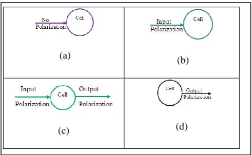
is calculated.Clocking is an important aspect of designing QCA device as well as QCA circuit. Four phases of clocking namely relax, switch, hold and release are used to design QCA device as well as QCA circuit. Each QCA cell must passes through all the phases of clocking. In relax phase, the QCA cell is in inactive state i.e., there is no polarization in the cell. In switch phase, the QCA cell gets polarized. The QCA cell stays sometimes its polarization in hold phase. In release phase, the QCA cell releases its polarization. The proposed PNN model explains the four phases of QCA clocking as shown in figure 3(a), 3(b), 3(c) and 3(d). In this proposed PNN model each QCA cell is represented by a process and is denoted by
41 4
1 0
,
4
1
n m
j m i n
j m i n r
Kink j i
r
r
q
q
E
© 2016, IRJET ISO 9001:2008 Certified Journal
Page 1004
circle. In the relax phase, no polarization is given to polarized the cell. In the switch phase, the polarization is given to activate or to polarize the cell. The polarization is holding for sometimes to propagate the polarization at output in hold phase. In release phase, once the polarization is propagated to output the cell releases its polarization. Different colours are used to show different phase of QCA clocking.
[image:2.595.36.285.195.340.2]Fig -1:(a) Polarization of QCA cells, (b) 3 input Majority Gate, (c) AND logic, (d) OR logic, (e) 5 input Majority Gate, (f) Triple Fan-out Butterfly tile
Fig -2:An artificial neuron as used in a Hopfield network
Fig -3: Proposed PNN model shows (a) relax phase, (b) switch phase, (c) hold phase, (d) release phase of QCA clocking
2. Error Calculation of a Circuit Using Proposed
Neural Network (PNN) Model
Irjet Template sample paragraph .Define abbreviations and acronyms the first time they are used in the text, even after they have been defined in the abstract. Abbreviations such as IEEE, SI, MKS, CGS, sc, dc, and rms do not have to be defined. Do not use abbreviations in the title or heads unless they are unavoidable.
To optimize the error in designing large/ complex QCA circuit it is important to calculate the error of each device. In this section, supervised training has done to calculate the error. The Root Mean Square (RMS) error calculation method has employed her e to examine the error of each device of the QCA circuit. There are two components to the error which are considered for supervised training. Firstly, the calculation of the error for each device for each training sets are processed. Secondly, the average of each sample for each training set has taken. After the processing of all training sets, the Root Mean Square (RMS) Error has computed by the following equation
n
Y
YBar
RMSE
n t t
12
(2)
where YBart for times t of a regression's dependent variable Y
is computed for n different predictions.
3. Proposed Neural Network Model (PNN) to Design
QCA Adder
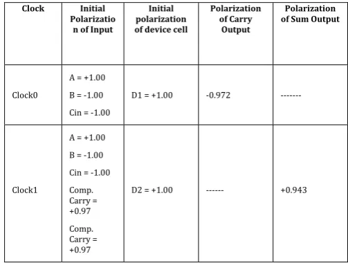
The proposed Neural Network model (PNN) has applied to design a reliable and robust one bit full adder circuit. The simulation result of proposed PNN model has given an error optimized and cost optimized result with respect to other simulation technique. An artificial intelligence based Hopfield Neural Network model has been proposed in this paper. The proposed PNN model has shown that the polarization of each output of the full adder circuit has given an acceptable precision. One three input majority gate and a five input majority gate are used to design the full adder circuit in this proposed PNN model. In this proposed PNN model two device cells and an inverter cell are used to design the full adder. The first device cell D1 is used to find the polarization of carry output and the second device cell D2 is used to find out the polarization of sum output of the full adder. The inverter cell is used to propagate the polarization with complement from first device cell D1 to second device cell D2. Two clocking zones are needed to design the single bit full adder circuit using proposed PNN model. The first device cell D1 has worked in one clocking zone (green color has used) and the second device cell has performed its task in the second clocking zone (pink color has used). The figure 4 shows the design architecture of one bit full adder using proposed PNN model. The following example has illustrated to explain the proposed PNN model. Suppose the full adder circuit adds two bits A=1 and B=0, so the output carry=0 and
(a) (b)
[image:2.595.37.254.396.497.2] [image:2.595.37.283.526.677.2]© 2016, IRJET ISO 9001:2008 Certified Journal
Page 1005
sum=1. The initial polarizations of both the inputs are set to +1.00 and -1.00 for A & B respectively and Cin is set to -1.00. In first clocking zone all the inputs polarization are imposed on the first device cell D1 and calculates the polarization of D1 through the Kink energy of the cell. Now, the polarization of device cell D1 has propagated to output carry through the Kink energy of the cell to find its polarization. This polarization of carry output is then transmitted to second device cell D2 through an inverter cell which complements the carry output. Now, the polarization of complemented carry output along with the initial polarization of all inputs are imposed on the second device cell D2 and calculate the polarization of D2 through the Kink energy of the cell. This calculated polarization of D2 has transmitted to output through the Kink energy of the cell to find out the polarization of sum output of the full adder circuit. The result of the proposed PNN model has shown better polarization at each output of the full adder compare to other simulation technique which helps to make large/ complex adder circuit in QCA. The better and acceptable precision of polarization at each output of the full adder helps to design robust and reliable QCA adder circuit. The simulation result of the single bit full adder has shown in table 1. The error can be optimized by using the proposed PNN model compare to other simulation technique. Optimization of error makes the circuit robust in structure and acceptable precision of polarization at each output makes the circuit more reliable. This full adder circuit helps to make large/ complex QCA adder as this full adder gives an acceptable precision of polarization at each output (Sum and Carry). The Ripple Carry Adder (RCA) has been designed using the proposed PNN model. The proposed PNN model has shown a better result compare to other simulation technique. The architecture of the RCA has shown in figure 5 using the proposed PNN model. This proposed PNN model has shown the correct output with an acceptable precision of polarization at output. To design a 4-bit RCA four full adder has been used in the proposed PNN model. Eight device cells (two in each full adder), four inverter (one in each full adder) has been used to design 4-bit RCA using proposed PNN model. The proposed PNN model has been used to add two 4-bit numbers. A3A2A1A0 is the first number (where A3 is MSB and A0 is LSB) which is added with B3B2B1B0 (where B3 is the MSB and B0 is the LSB). Assumed that A3A2A1A0=1010 and B3B2B1B0=0110 are to be added. So that the input polarization A0=-1.00 (as it takes 0), B0=-1.00 (as it takes) and Cin=-1.00 (as it takes 0) have been imposed to the first device cell of the first full adder. The first device cell then calculates the polarization of the first device cell of the first full adder D1 and has been transferred to the output through the Kink energy of the cell. The polarization of the device cell helps to find the polarization of output cell of carry output. The complement polarization of the device cell D1 is then imposed through an inverter cell I1 on the second device cell of the full adder D2 along with all three inputs polarization to calculate the polarization of sum (S0) output of the first full adder. The polarization of the carry output C0 of the first full
[image:3.595.309.558.358.447.2]adder is imposed on the first device cell of the second full adder D3 along with the polarization of input A=+1.00 (as it takes 1) and B=-1.00 (as it takes 0) and find the polarization of the device cell D3. The polarization of the device cell D3 is then propagated through the Kink energy of the cell to the output cell to find the polarization of carry output C1 of the second full adder. Now, the complemented polarization of C1 is imposed via an inverter I2 on the second device cell of the second full adder D4 along with the polarization of inputs A1 and B1 which helps to find the polarization of the device cell D4. The polarization of the device cell D4 is then propagated to output cell through the Kink energy of the device cell D4 to find the polarization of sum (S1) of the second full adder and so on. The final output of the 4-bit RCA is C3S3S2S1S0=10000 with the polarization C3=+0.972, S3=-0.943, S2=-0.943, S1=-0.943, S0=-0.943. The proposed PNN model has given acceptable precision of polarization at each output of the 4-bit RCA. Errors are being optimized using the proposed PNN model and also the robust and reliable circuit can be designed using this proposed PNN model. The large circuit has also been designed using this proposed model.
Fig -4: Proposed PNN model of single bit full adder
Table -1:Simulation Result of Single bit full adder circuit
Clock Initial Polarizatio
n of Input
Initial polarization of device cell
Polarization of Carry
Output
Polarization of Sum Output
Clock0
A = +1.00 B = -1.00 Cin = -1.00
D1 = +1.00 -0.972 ---
Clock1
A = +1.00 B = -1.00 Cin = -1.00 Comp. Carry = +0.97 Comp. Carry = +0.97
[image:3.595.309.561.493.683.2]© 2016, IRJET ISO 9001:2008 Certified Journal
Page 1006
Fig -5: Proposed PNN model of 4-bit Ripple Carry Adder
4. RESULTS & DISCUSSIONS
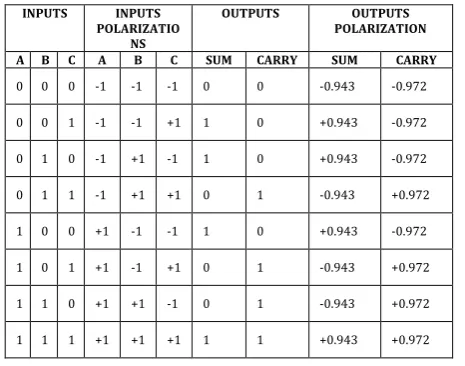
[image:4.595.40.273.488.671.2]The simulation result of the proposed PNN model has given acceptable precision of polarization at each output of single bit full adder as well as large/ complex QCA adder circuit. The simulation of the single bit full adder as well as large/ complex QCA adder using the proposed PNN model has done with a set of training data and tested with the actual output of the adder. The table 2 has shown the training sample of single bit full adder circuit. The following table 1 has shown the output polarization of each output (SUM & CARRY) for all possible polarization of inputs. The sign bit of the polarization shows whether the output value is ‘0’ or ‘1’. The (-) ve polarization at output represents ‘0’ as output value and (+) ve sign in polarization represents ‘1’ as output value. The sample training data for 4-bit RCA has shown in table 3. The result of 4-bit RCA can help to make more large/ complex QCA adder circuit design.
Table 2:Training sample data of single bit full adder circuit
5. CONCLUSIONS
QCA is an emerging technology in the era of nanotechnology. Artificial intelligence technique is used to find the error free QCA adder circuit design. The proposed PNN model is presented in this paper to design error optimized and simulation of the QCA adder circuit. This result of proposed PNN model gives the most robust and reliable QCA adder circuit. The proposed PNN model simulation gives an acceptable precision of polarization at each output of the adder circuit. It has been concluded that more large/ complex QCA adder circuit can be designed by this proposed PNN model. The accuracy of polarization at each output is given by this proposed PNN model. The proposed PNN model is applied on some QCA adder circuit to analyze the performance of the proposed PNN model. The efficiency, accuracy and performance are the advantage of using this proposed PNN model. The robust and reliable structure of QCA adder circuit can be found using this proposed PNN model.
INPUTS INPUTS POLARIZATIO
NS
OUTPUTS OUTPUTS POLARIZATION A B C A B C SUM CARRY SUM CARRY
0 0 0 -1 -1 -1 0 0 -0.943 -0.972
0 0 1 -1 -1 +1 1 0 +0.943 -0.972
0 1 0 -1 +1 -1 1 0 +0.943 -0.972
0 1 1 -1 +1 +1 0 1 -0.943 +0.972
1 0 0 +1 -1 -1 1 0 +0.943 -0.972
1 0 1 +1 -1 +1 0 1 -0.943 +0.972
1 1 0 +1 +1 -1 0 1 -0.943 +0.972
1 1 1 +1 +1 +1 1 1 +0.943 +0.972
PO LA R IZ A T IO N O F EA CH O U T PU T C3 S 3 S 2 S 1 S0 -0.97 2 + 0.94 3 -0.94 3 -0.94 3 + 0.94 3 -0.97 2 + 0.94 3 -0.94 3 + 0.94 3 + 0.94 3 -0.97 2 + 0.94 3 + 0.94 3 + 0.94 3 + 0.94 3 +0 .972 -0.94 3 -0.94 3 -0.94 3 +0 .943 +0 .972 +0 .943 -0.94 3 -0.94 3 -0.94 3 O U T PU T C3S 3S 2S 1S 0
0 1 0
0 1
0 1 0
1 1
0 1 1
1
1
1 0 0
0 1
1 1 0
0 0
IN PU T S PO LA R IZ A T IO N B3B 2B1B 0 +1 -1
-1 +1
-1+1 +1
-1
-1
-1 +1 +1
+1
-1
-1 +1
+1 +1 +1 +1
A 3A 2A 1 A 0 -1 -1 -1 -1 -1+1
-1 +1
+1 +1
-1 -1 +1 -1 -1 -1 +1 -1
-1 +1
IN PU T S B3B 2B1B 0
1 0 0
1
0 1 1 0 0 0 1
1
1 0 0 1 1 1
1 1
A 3A 2A 1 A 0
© 2016, IRJET ISO 9001:2008 Certified Journal
Page 1007
REFERENCES
[1] International technology roadmap for semiconductors: 2001, Semiconductor Industries Association, San Jose, CA, http://public.itrs.net
[2] C.S. Lent, P.D. Taugaw, W. Porod, and G.H. Bernstein “Quantum dot cellular automata,” Nanotechnology 4 (1993): 49–57.
[3] Kunal Das, and Debashis De. "Characterisation, applicability and defect analysis for tiles nanostructure of quantum dot cellular automata." Molecular Simulation 37.03 (2011): 210-225.
[4] Mohsen Hayati, and Abbas Rezaei. "New approaches for modeling and simulation of quantum-dot cellular automata." Journal of Computational Electronics 13.2 (2014), pp. 537-546.
[5] Omar Paranaiba Vilela Neto, Marco Aurélio Cavalcanti Pacheco, and Carlos R. Hall Barbosa. "Neural network simulation and evolutionary synthesis of QCA circuits." Computers, IEEE Transactions on 56.2 (2007), pp. 191-201.
[6] John J. Hopfield. "Neural networks and physical systems with emergent collective computational abilities." Proceedings of the national academy of sciences 79.8 (1982), pp. 2554-2558.
[7] John J. Hopfield "Neurons with graded response have collective computational properties like those of two-state neurons." Proceedings of the national academy of sciences 81.10 (1984), pp. 3088-3092.
[8] John J. Hopfield and David W. Tank. "“Neural”
computation of decisions in optimization problems." Biological cybernetics 52.3 (1985), pp. 141-152.
BIOGRAPHIES