Partial Discharge Simulation under Various Applied
Voltage Waveforms
Hazlee Illias, Low Tau Jian, Ab Halim Abu Bakar, Hazlie Mokhlis
Electrical Engineering Department, UMPEDACFaculty of Engineering, University of Malaya Kuala Lumpur, Malaysia
Abstract—In high voltage power equipment, partial discharge (PD) measurement is widely used in the performance assessment of an insulation system. However, from modelling of PD, a better understanding of the phenomenon may be attained. PD activity within a void in a solid dielectric insulation material is influenced by many factors. One of the factors is the applied voltage. Different types of the applied voltage yield in different PD patterns and the condition for breakdown of insulation to occur. In this work, PD activity under various types of the applied voltages has been studied. A finite element analysis (FEA) software was used to simulate PD occurrence within a void in a dielectric material. The applied voltages that were considered are AC sinusoidal, damped AC and impulse voltages. PD patterns were observed through phase resolved partial discharge (PRPD) patterns. The obtained result may improve an understanding on PD behaviour under different types of the applied voltage. It may also assist in insulation diagnostics and performance assessment of an insulation system.
Keywords-partial discharge; condition monitoring; finite element analysis; electrical insulation
I. INTRODUCTION
In high voltage equipment, the build-up of charge and its by-products can be symptomatic of problems associated with aging and insulation breakdown. If such problems are not repaired, the strength and frequency of partial discharge (PD) increase, which eventually leads to the catastrophic failure of the high voltage equipment [1]. This may cause external equipment damage, resulting in a high repair cost due to an unscheduled outage. Therefore, a reliable online PD detection is important and is a must for power companies to improve the safety and decrease the potential of plant shut down. This is one of the reasons why PD detection is used in power systems to monitor the condition of high voltage equipment.
One of the factors which influences PD activity within insulation system of high voltage equipment is the applied voltage waveform. PD activity within a spherical void in a dielectric material under AC sinusoidal applied voltage has been studied through measurement and simulation [2-5]. The results found that at higher frequency and amplitude of the applied voltage, the number of PDs per cycle and the total PD charge per cycle increase. PD patterns were found to follow the waveform of the sinusoidal voltage. There were two
distinguished patterns formed, a ‘rabbit-ear’ and ‘tortoise like’ patterns. These patterns were due to the difference in the difficulty of electron detrapping from the void surface with different polarity of charges accumulated on it. Simulation of PD was performed and compared to the measurement results. From comparison, critical parameters influencing PD activity under AC sinusoidal applied voltage have been successfully identified.
PD mechanism in a silicone gel has been studied through experiment under AC sinusoidal and impulse voltages in a point plane geometry [6]. Under impulse applied voltage, PD behaviour shows that the first discharges recorded in a silicon gel were due to the initiation and propagation of streamers. However, under AC applied voltage, a stable PD regime rapidly establishes, where a streamer creates a void with a long lifetime and PDs occur in the void during the subsequent voltage cycle. This resulted in permanent degradations of the gel due to the repetition of PDs. These findings clearly indicate that PD mechanism is strongly influenced by the applied voltage conditions.
In this paper, PD activity within a void in a dielectric material under various types of the applied voltages has been studied through simulation. A PD model and finite element analysis (FEA) software were used to simulate PD events. Phase resolved partial discharge (PRPD) patterns were used to observe PD patterns. The applied voltages that were simulated are AC sinusoidal, damped AC and impulse voltages. From the study of PD events under different applied voltages, PD activity can be characterised more precisely and critical parameters affecting PD activity under different types of applied voltage can be identified. This may assist in performance assessment and diagnostics of insulation system.
II. PARTIALDISCHARGEMODELEQUATIONS
The first condition for a PD to occur within a void in a dielectric material is the electric field in the void,Evoidmust be
larger than the inception field,Einc.Eincis calculated using [7]
Einc= 25.2P[1+ 8.6/(2Pr)0.5] (1)
The second condition for a PD to occur is a starting electron is needed to start ionization. The supply of an initial electron influences the statistical characteristics of PD activity such as the inception delay, the number of PD occurrences and distributions with respect to the applied voltage. In a virgin void, a starting electron may be provided by natural high energetic radiation via photo ionization in the gas or by photo ionization in the insulation. The starting electrons can also be produced by field emission from the void surface if its effective work function is low [7, 8].
For a void which has never experienced PD, volume ionization is the main source of an initial free electron. If the void consists of air, the rate of volume ionization can be calculated using [7, 8]
Nv= 20P(πab2)(1-v-2) (2)
where a and b are the height and radius of the void. v is the ratio of the applied voltage to the inception voltage or the overvoltage ratio [7],
v=U0/U0inc (3)
where U0 is the maximum applied voltage and U0inc is the
inception voltage.
After the first PD has occurred, an additional source of initial electron becomes available through charges along the void surface from the previous PD. A free initial electron emitted from the void surface,Ṅdtcan be expressed as [7]
Ṅdt=Ndtvoexp(-[ϕ-√[eEvoid/(4πɛ0)]/(kT)]) (4)
where Ṅdt is the number of electrons available for being
detrapped,vois the fundamental phonon frequency (≈1014Hz),
eis the elementary charge, Ф is the effective detrapping work function, ε0is the permittivity of vacuum,kis the Boltzmann
constant and T is the temperature (in Kelvin). Ndt is the
detrappable electrons from the surface due to previous PD, which decays between consecutive PDs. It has been defined as [7]
Ndt=Ndt0exp(-t/τ) (5)
wheretis the time elapsed since the last PD event andτis the effective charge decay time constant.Ndt0has been assumed to
be proportional to the number of charges,qdue to PD [7],
Ndt0=ξ(q/e) (6)
q=ε0πb2[1+εr(K-1)]∆E (7)
whereξ is the proportionality factor,b is the void radius,εris
the material permittivity, ∆E is the field collapse in the void after a PD occurs andKequals to 3 for a spherical void. ∆Eis
∆E=EvoidnoPD+Eq-Eext (8)
whereEvoidnoPDis the field in the void in the absence of PD,Eq
is the field due to charges on the void surface after a PD has occurred andEextis the extinction field.
The proportionality factor,ξdepends on the polarity of the surface charge from which electron detrapping occurs. This is because the negative and positive charges on the void surface have a different efficiency of allowing electrons to detrap form the void surface [7]. An electron detraps from negative surface charges after the polarity ofEvoidchanges between consecutive
PDs but not when the surface charges are negative.
The total number of electrons,Ntavailable to initiate a PD
is equal to
Nt=Ṅdt+Nv (9)
A PD occurrence is a random process. Thus, the probability,Pof a PD to occur is defined asNt∆t, where ∆tis
the time step of the simulation. A PD will only occur if Pis larger than a random number,R, which is between 0 and 1.
The dipolar charges due to the PD induce charges on the conductors on the insulation material. These charges are called the apparent charge, q’ [7, 8]. For a plane-parallel electrode with a gap distance ofDand void radius ofa,q’equals to
q’= (4/3)πab2ε
0εrK∆E/D (10)
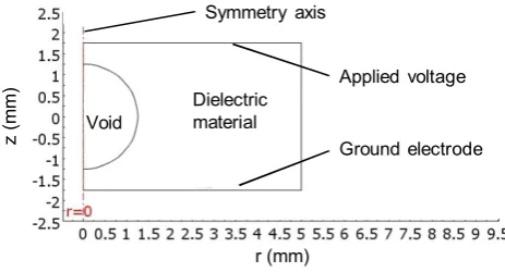
III. MODELGEOMETRY
A two-dimensional (2D) axial-symmetric model geometry consists of a spherical void and a cylindrical dielectric material has been developed using finite element analysis (FEA) software, as shown in Figure 1. The model has been used to obtain the electric field in the void,EvoidnoPDin the absence of
PD through simulation of the electric field distribution in the model. The obtained value was used in (8) for the applied voltage of 19.25 kV. The parameters used for the simulation are summarised in Table 1 and were chosen based on the literature [7].
r (mm)
z
(m
m
)
Void Dielectricmaterial
Ground electrode Symmetry axis
Applied voltage
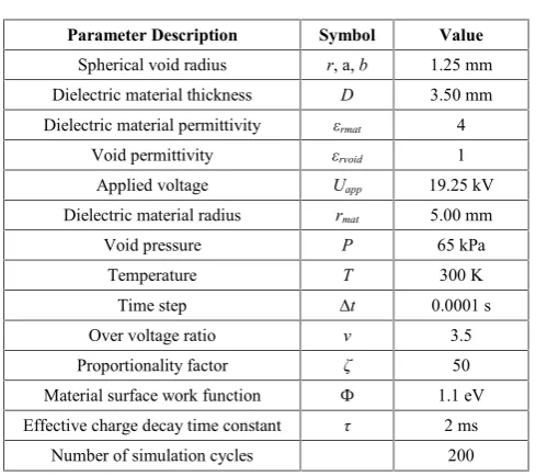
[image:2.595.315.547.542.667.2]TABLE I. BOUNDARYCONDITIONS OF THEMODEL
Parameter Description Symbol Value
Spherical void radius r, a,b 1.25 mm
Dielectric material thickness D 3.50 mm
Dielectric material permittivity εrmat 4
Void permittivity εrvoid 1
Applied voltage Uapp 19.25 kV
Dielectric material radius rmat 5.00 mm
Void pressure P 65 kPa
Temperature T 300 K
Time step ∆t 0.0001 s
Over voltage ratio v 3.5
Proportionality factor ζ 50
Material surface work function Ф 1.1 eV
Effective charge decay time constant τ 2 ms
Number of simulation cycles 200
IV. SIMULATIONRESULTS
A. PD under AC sinusoidal applied voltage
Figure 2 shows the electric field magnitude as a function of time of 50 Hz, 19.25 kV sinusoidal applied voltage obtained using FEA and PD model equations for the first two cycles. When the electric field within the void, Evoid exceeds the
inception field, Einc and if there is a free initial electron
available, a PD will occur, causing Evoidto drop less than the
extinction field, Eext. If there is no PD occurs at all,Evoidwill
follow the curve of EvoidnoPD, which is the electric field in the
void without any surface charge due to PD. At the time between 0.005s and 0.01s, PD does not occur immediately when Evoidis higher than the inception field there is no free
initial electron available for a PD to occur. This delay is called the statistical time lag,τstat.
For PD activity under AC sinusoidal voltage, there are two different types of statistical time lag. The first type isτstatdue to
the first PD. This time lag is long because electrons are harder to be emitted from the void surface due to the absence of electron accumulating on the void surface. Electrons are likely to be available from volume ionisation. The second type ofτstat
is τstat after the previous PD has occurred. This time lag is
shorter because there are more free electrons available on the void surface after the previous PD has occurred. The statistical time lag influences the number of PDs per cycle.
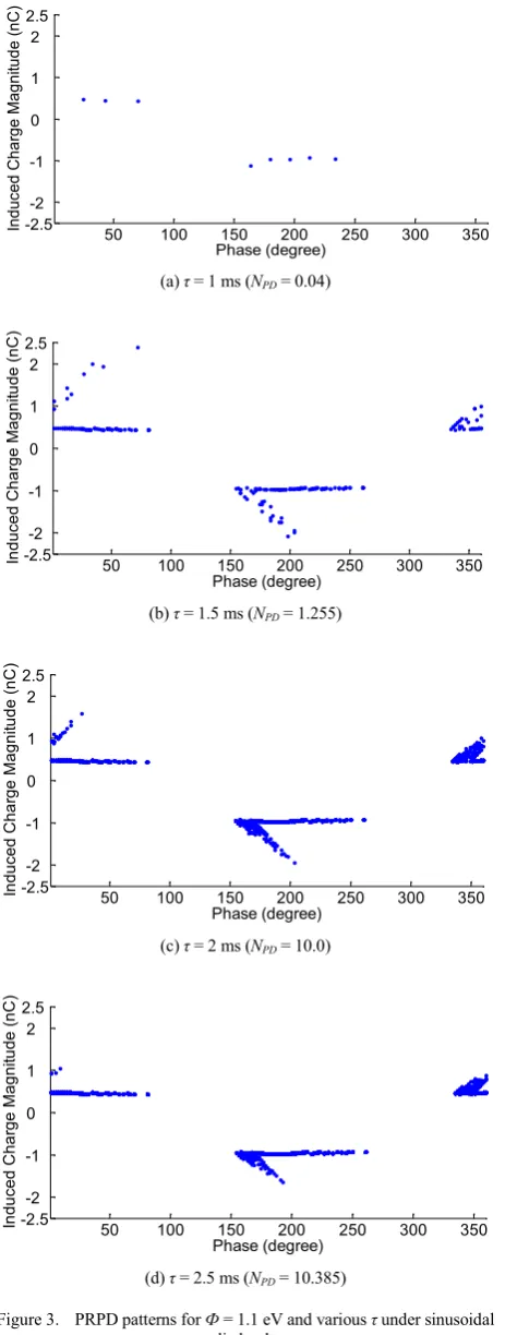
One of the factors which influences the PD activity within a void in a dielectric material is the effective charge decay time constant,τ. To study the effect of this parameter, the material surface work function, Ф is fixed at 1.1 eV but τ is varied from 1 ms to 3 ms in (5). The phase resolved partial discharge (PRPD) patterns are used to observe PD patterns under different parameters of the simulation and conditions of the applied voltage.
0 0.005 0.01 0.015 0.02 0.025 0.03 0.035 0.04 -8
-6 -4 -2 0 2 4 6 8x 10
6
time(s)
Ev
oi
d,
Ei
nc
,E
vo
id
no
pd
(V
/m
)
Evoid,Einc,Evoidnopd(V/m)versus t(s)
Evoid
Evoidnopd
Einc
El
ec
tri
c
fie
ld
(
kV/
m
m
)
Time (s)
EvoidnoPD
Evoid
Einc
Figure 2. Electric field magnitude against time of sinusoidal applied voltage
A PRPD pattern shows the occurrence of PDs at a specific phase of the applied voltage (in degree) with a certain charge magnitude (in nC), as represented by the ‘dots’ in Figure 3. In a PRPD pattern, PDs occurring in certain number of applied voltage cycle are grouped together into one applied voltage cycle, ranging from 0 to 360 degrees. If more PDs occur within an applied voltage cycle, more ‘dot’ can be seen in a PRPD pattern. PRPD patterns are commonly used in condition monitoring of high voltage equipment to observe PD activity.
From Figure 3, the PRPD patterns change significantly whenτ is varied. Whenτis increased, the number of PDs per cycle, NPD increases. τ controls the rate of charges that have
accumulated on the void surface due to previous PD to decay with time. From (4), when τis larger, the electron detrapping due to surface emission, Ṅdtbecomes higher. This is due to a
longer τ causes the accumulated charges on the void surface due to previous PD to decay slower with time. Thus, the total number of electrons, Nt available to initiate the next PD is
higher, resulting in a higher probability of a PD to occur when the inception field,Eincin the void is exceeded. This results in
PD to occur almost immediately afterEinchas been exceeded,
yielding the maximum PD charge magnitude to decrease with longer τ and more PDs occurring at lower PD charge magnitudes. A lower charge magnitude is obtained when a PD occurs at a lower electric field in the void.
B. Damped AC sinusoidal applied voltage
The mathematical expression of a damped AC sinusoidal applied voltage waveform can be represented by the product of an AC sinusoidal waveform and the inverse of exponential,
U=Uappsin(2πft)e-t/τd (11)
where f is the frequency, t is the time and τd is the decay
constant of the waveform. To study the effect of damped AC sinusoidal voltage on PD activity within a void in a dielectric material, the applied frequency is set at 50 Hz whileτdis varied
[image:3.595.41.286.65.282.2]50 100 150 200 250 300 350 -2.5
-2 -1 0 1 2 2.5
Phase (degree)
In
du
ce
d
C
ha
rg
e
M
ag
ni
tu
de
(n
C
) Induced Charge Magnitude (nC) vs Phase (degree)
(a)τ= 1 ms (NPD= 0.04)
50 100 150 200 250 300 350
-2.5-2 -1 0 1 2 2.5
Phase (degree)
In
du
ce
d
C
ha
rg
e
M
ag
ni
tu
de
(n
C
) Induced Charge Magnitude (nC) vs Phase (degree)
(b)τ= 1.5 ms (NPD= 1.255)
50 100 150 200 250 300 350
-2.5-2 -1 0 1 2 2.5
Phase (degree)
In
du
ce
d
C
ha
rg
e
M
ag
ni
tu
de
(n
C
) Induced Charge Magnitude (nC) vs Phase (degree)
(c)τ= 2 ms (NPD= 10.0)
50 100 150 200 250 300 350
-2.5-2 -1 0 1 2 2.5
Phase (degree)
In
du
ce
d
C
ha
rg
e
M
ag
ni
tu
de
(n
C
) Induced Charge Magnitude (nC) vs Phase (degree)
(d)τ= 2.5 ms (NPD= 10.385)
Figure 3. PRPD patterns forФ= 1.1 eV and variousτunder sinusoidal
applied voltage
Figure 4 shows the plot of electric field as a function of time of the damped AC applied voltage. The curve is similar to Figure 2, except that the maximum applied voltage amplitude decreases with time.
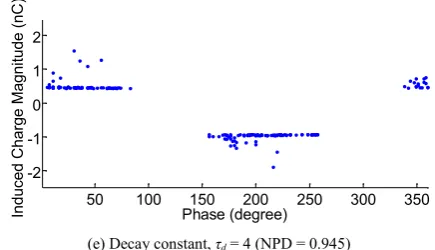
The PRPD patterns under damped AC sinusoidal applied voltage when the decay constant, τd is varied are shown in
Figure 5. When the decay constant of the damped AC waveform is increased, the number of PD per cycle, NPD
decreases. This is because the magnitude of the electric field within the void decreases faster with time, which can be seen in the figure of the electric field plot as a function of time. Thus, the magnitude of the electric field in the void becomes less than the inception field at earlier time, preventing any PD from reoccurring. It can also be seen that the number of PDs found at the ‘curvy’ shape of the PRPD patterns under damped AC voltage is lower when the decay constant increases. In general, the pattern of PD activity under damped AC sinusoidal voltage is similar under the applied sinusoidal voltage. However, the ‘curvy’ shape of the PRPD pattern becomes less obvious when the decay constant is higher. The maximum PD charge magnitude also decreases under higher decay constant of the damped AC applied voltage.
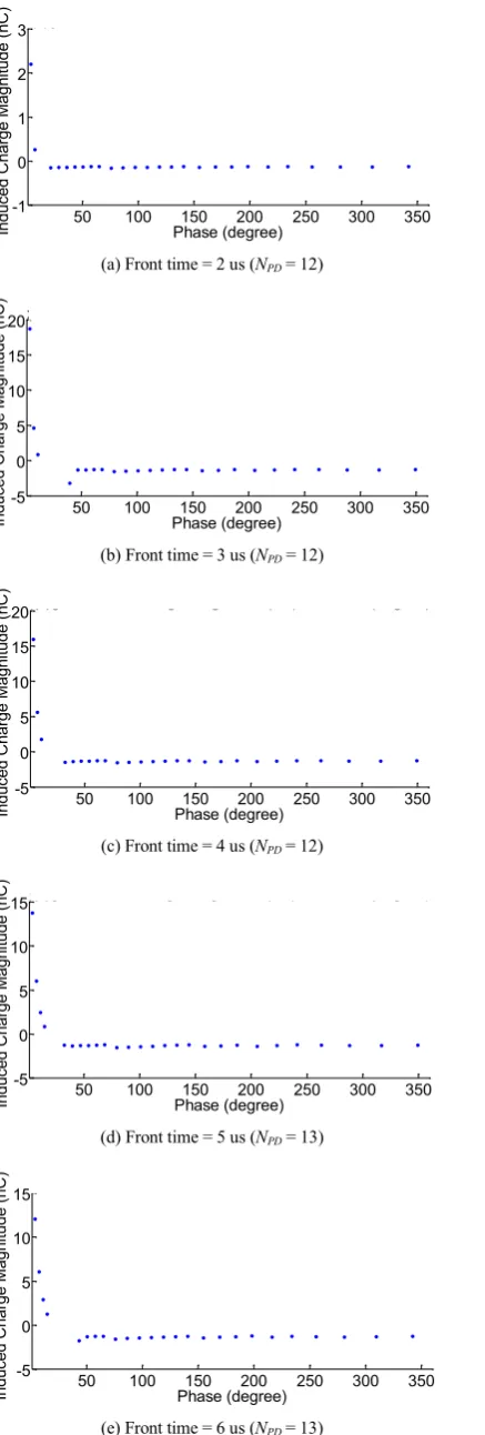
C. Impulse applied voltage
Separated double exponential function can be used to represent an impulse voltage, which is represented by
U=Uapp[exp(-(t-t0)/τ2) - exp(-(t-t0)/τ1)] (12)
whereτ1andτ2are the time constant andt0is the true origin of
the impulse.
The model geometry and parameters that have been used for simulation of PD activity under impulse voltage is the same as in Figure 1 and Table 1. Figure 6 shows the electric field magnitude plot as a function of time of the impulse voltage, The applied voltage,Uappis 50 kV,t0is zero andτ1andτ2are
1.2 us and 50 us. PDs can be seen to occur very frequently at the front time of the impulse voltage but less frequent at the tail time.
0 1 2 3 4
-1 -0.5 0 0.5
1x 10
7
time(s)
E
vo
id
,E
in
c,
E
vo
id
no
pd
(
V
/m
) Evoid,Einc,Evoidnopd(V/m)versus t(s)
EvoidnoPD
Evoid
Einc
El
ec
tri
c
fie
ld
(
x1
0
7V/
m
)
Time (s)
[image:4.595.50.282.61.674.2] [image:4.595.321.546.532.652.2]50 100 150 200 250 300 350 -2
-1 0 1 2
x 10-9
Phase (degree)
In
du
ce
d
C
ha
rg
e
M
ag
ni
tu
de
(n
C
)
Induced Charge Magnitude (nC) vs Phase (degree)
(a) Decay constant,τd= 0.25 (NPD= 8.415)
50 100 150 200 250 300 350
-2 -1 0 1 2
x 10-9
Phase (degree)
In
du
ce
d
C
ha
rg
e
M
ag
ni
tu
de
(n
C
)
Induced Charge Magnitude (nC) vs Phase (degree)
(b) Decay constant,τd= 0.5 (NPD= 4.965)
50 100 150 200 250 300 350
-2 -1 0 1 2
x 10-9
Phase (degree)
In
du
ce
d
C
ha
rg
e
M
ag
ni
tu
de
(n
C
)
Induced Charge Magnitude (nC) vs Phase (degree)
(c) Decay constant,τd= 1 (NPD= 2.86)
50 100 150 200 250 300 350
-2 -1 0 1 2
x 10-9
Phase (degree)
In
du
ce
d
C
ha
rg
e
M
ag
ni
tu
de
(n
C
)
Induced Charge Magnitude (nC) vs Phase (degree)
(d) Decay constant,τd= 2 (NPD= 1.68)
50 100 150 200 250 300 350
-2 -1 0 1 2
x 10-9
Phase (degree)
In
du
ce
d
C
ha
rg
e
M
ag
ni
tu
de
(n
C
) Induced Charge Magnitude (nC) vs Phase (degree)
(e) Decay constant,τd= 4 (NPD = 0.945)
Figure 5. PRPD patterns for different decay constant under damped AC sinusoidal applied voltage
0 0.2 0.4 0.6 0.8 1 1.2
x 10-4 -5
0 5 10 15 20x 10
6
time(s)
Ev
oi
d,
Ei
nc
,E
vo
id
no
pd
(V
/m
)
Evoid,Einc,Evoidnopd(V/m)versus t(s)
E
le
ct
ric
fi
el
d
(k
V
/m
m
)
Time (x10-4s)
EvoidnoPD
Evoid
Einc
0 0.2 0.4 0.6 0.8 1 1.2
x 10-4 -5
0 5 10 15 20x 10
6
time(s)
Ev
oid
,E
inc
,E
vo
idn
op
d
(V
/m
)
Evoid,Einc,Evoidnopd(V/m)versus t(s)
Figure 6. Electric field magnitude as a function of time of an impuse voltage
[image:5.595.323.541.56.181.2] [image:5.595.315.548.229.423.2]50 100 150 200 250 300 350 -1
0 1 2 3x 10
-8
Phase (degree)
In
du
ce
d
C
ha
rg
e
M
ag
ni
tu
de
(n
C
) Induced Charge Magnitude (nC) vs Phase (degree)
(a) Front time = 2 us (NPD= 12)
50 100 150 200 250 300 350
-5 0 5 10 15 20x 10
-9
Phase (degree)
In
du
ce
d
C
ha
rg
e
M
ag
ni
tu
de
(n
C
) Induced Charge Magnitude (nC) vs Phase (degree)
(b) Front time = 3 us (NPD= 12)
50 100 150 200 250 300 350
-5 0 5 10 15 20x 10
-9
Phase (degree)
In
du
ce
d
C
ha
rg
e
M
ag
ni
tu
de
(n
C
)
Induced Charge Magnitude (nC) vs Phase (degree)
(c) Front time = 4 us (NPD= 12)
50 100 150 200 250 300 350
-5 0 5 10 15x 10
-9
Phase (degree)
In
du
ce
d
C
ha
rg
e
M
ag
ni
tu
de
(n
C
)
Induced Charge Magnitude (nC) vs Phase (degree)
(d) Front time = 5 us (NPD= 13)
50 100 150 200 250 300 350
-5 0 5 10 15x 10
-9
Phase (degree)
In
du
ce
d
C
ha
rg
e
M
ag
ni
tu
de
(n
C
) Induced Charge Magnitude (nC) vs Phase (degree)
V. CONCLUSIONS
Partial discharge (PD) behaviour under different applied voltages has been studied through simulation model in this work. PD behaviour was observed through phase resolved partial discharge (PRPD) patterns under AC sinusoidal, damped AC sinusoidal and impulse applied voltages. PD activity within a void in a dielectric material is strongly influenced by the applied voltage waveform because the electric field magnitude in the void is determined by the applied voltage. The maximum electric field in the void was calculated through a model geometry that has been developed using finite element analysis (FEA).
For PD activity under AC sinusoidal applied voltage, when the effective charge decay time constant increases, the number of PDs per cycle was found to increase. When the decay constant of the damped AC sinusoidal waveform increases, the number of PDs per cycle decreases. PRPD patterns changes with the change of the decay constant of the damped AC sinusoidal applied voltage. The number of PDs occurring within the front time of an applied impulse voltage increases when the front time is longer.
Future work will consider the actual experiment of PD activity under different applied voltage waveform. The measurement results will then be compared with the simulation results to identify critical parameters affecting PD activity under various types of the applied voltage.
ACKNOWLEDGMENT
The author thanks the University of Malaya for supporting this work through the HIR research grant (Grant no: H-16001-00-D000048).
REFERENCES
[1] E. Kuffel, W. S. Zaengl, and J. Kuffel, High Voltage Engineering:
Fundamentals, 2nd ed.: Newnes, Butterworth-Heinemann, 2000. [2] H. Illias, G. Chen, and P. L. Lewin, "Partial Discharge within a Spherical
Cavity in a Dielectric Material as a Function of Cavity Size and Material
Temperature,"IET Science, Measurement & Technology,pp. 1-8, 2012.
[3] H. Illias, G. Chen, and P. L. Lewin, "The influence of spherical cavity surface charge distribution on the sequence of partial discharge events,"
Journal of Physics D: Applied Physics,vol. 44, pp. 1-15, 2011. [4] H. Illias, G. Chen, and P. L. Lewin, "Modeling of partial discharge
activity in spherical cavities within a dielectric material," IEEE
Electrical Insulation Magazine,vol. 27, pp. 38-45, 2011.
[5] H. Illias, G. Chen, and P. L. Lewin, "Partial Discharge Behavior within a Spherical Cavity in a Solid Dielectric Material as a Function of
Frequency and Amplitude of the Applied Voltage,"IEEE Transactions
on Dielectrics and Electrical Insulation,vol. 18, pp. 432-443, 2011. [6] T. Do, O. Lesaint, and J. L. Auge, "Streamers and partial discharge
mechanisms in silicone gel under impulse and AC voltages," IEEE
Transactions on Dielectrics and Electrical Insulation,vol. 15, pp. 1526-1534, 2008.
[7] L. Niemeyer, "A generalized approach to partial discharge modeling,"
IEEE Transactions on Dielectrics and Electrical Insulation,vol. 2, pp. 510-528, 1995.
[8] F. Gutfleisch and L. Niemeyer, "Measurement and simulation of PD in
epoxy voids," IEEE Transactions on Dielectrics and Electrical
[image:6.595.67.286.51.698.2]