HEWLETT-PACKARD
CONFIDENTIAL
DIO BUS SPECIFICATION
VERSION 1.0
APRIL 1 6, 1984
HP DRAWING NO: 5955-7669
DOCUMENT CONTROL
CHANGES'TO"THIS DOCUMENT SHOULD BE .
COORDINATED THROUGH THE RND R&D LAB.,
DISTRIBUTION
010 BUS SPECIFICATION
PRINTING HISTORY
First draft: December
14, 1982
Second draft: March 27,
1983
Version
1.0:
April16, 1984
Copyright ~ Hewlett-Packard Co.
1984
This material contains proprietary information protected by
copyright laws. Any reproduction, photocopying or translation of
any portion of this document to any foreign or computer language
DIO BUS SPECIFICATION
TABLE OF CONTENTS
CHAPTER 1 FOREWARD . . . 1
CHAPTER 2 INTRODUCTION
2.1 OBJECTIVES OF THE DIO BUS SPECIFICATION. . 2
2.2 PROCEDURE FOR RESOLVING CHANGES. . . .
3
2.3 WHAT IS NOT COVERED IN THIS DOCUMENT . 3
2.4
RECOMMENDED DESIGN METHODOLOGY.4
CHAPTER 3 DIO BUS BACKGROUND INFORMATION
3.1 SPECIFICATION TERMINOLOGY. 3.2 INTERFACE SYSTEM ELEMENTS.
3.3
BUS SUBSYSTEMS . . . . .3.4
BUS TIMING BACKGROUND . . .5
6
8 9CHAPTER
4
I/O MEMORY MAP AND I/O CARD REGISTERS4.1
SERIES 200 MEMORY MAP . .4.2
E~TERNAL I/O MEMORY MAP.4.3
I/O CARD REGISTERSCHAPTER
5
DATA TRANSFERS5·1
5·2
5·3
5.4
5·5
5.6
5.7
5.8
DATA TRANSFER SIGNALS . . . OVERVIEW OF THE DATA TRANSFER. READ CYCLE . . . .
WRITE CYCLE. . . . READ-MODIFY-WRITE. . . . ENDT OVERVIEW . . . . READ CYCLE USING ENDT . . WRITE CYCLE USING ENDT .
CHAPTER 6 BUS ERROR AND STRETCH OPERATION
6.1
6.2
6.3
6.4
6.5
BUS ERROR SIGNALS. . . . BERR TIMING. . . . BUS TIMEOUT. . . . AUTO LOCATE OF PROCESSOR RAM . BERR FOR PAGE FAULTING . . . .
· . 13
· . 14
· . 15
· . . 19
. . . 20 · . . 22 · . . 27 · . • 28
. 31
. 33· . . 35
010 BUS SPECIFICATION
CHAPTER 7 INTERRUPT OPERATION
7.1 INTERRUPT SIGNALS . . . .
7.2 EXTERNAL VECTORED INTERRUPT CYCLE.
7.3 AUTOVECTORED INTERRUPT CYCLE
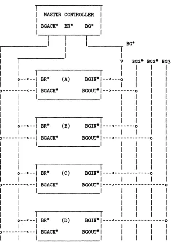
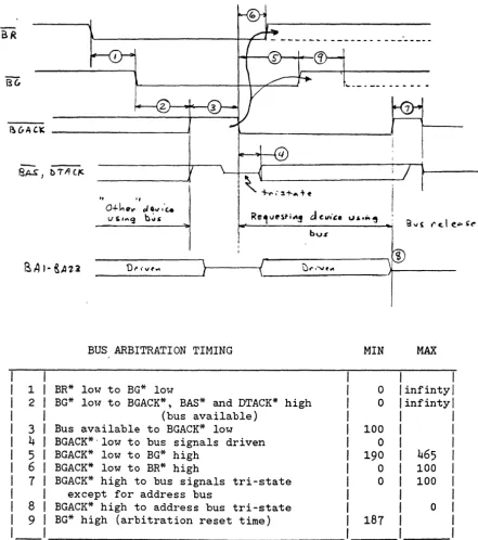
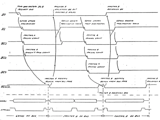
CHAPTER 8 BUS ARBITRATION
8.1 BUS ARBITRATION SIGNALS . .
8.2
BUS ARBITRATION OVERVIEW.8.3
BUS ARBITRATION SEQUENCE .CHAPTER 9 DMA OPERATION
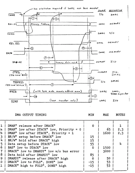
9.1
9.2
9·3
9.4
9·5
9.6
9.7
DMA SIGNALS . . . DMA OVERVIEW . .
98620
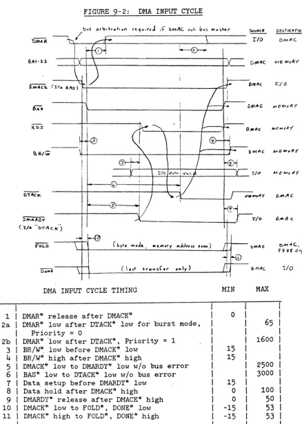
DMA CONTROLLERDMA OUTPUT CYCLE . . DMA INPUT CYCLE . . . DMA SPEED CONSIDERATIONS . TERMINATING DMA TRANSFERS.
CHAPTER 10 DIO BUS UTILITIES
10.1 BUS DRIVE DISABLE . . . . .
10.2
RESET OPERATION . . . .10.3 HALT OPERATION . . . .
10.4 FUNCTION CODE SIGNALS.
CHAPTER 11 ELECTRICAL SPECIFICATIONS
11.1 POWER DISTRIBUTION AND GROUNDING . 11.2 POWER SUPPLY TOLERANCES . . .
11.3 I/O CARD CURRENT REQUIREMENTS . .
11.4 ON-CARD FUSE SPECIFICATION.
11.5 SIGNAL LOADING . . . .
· . 41 · . 43 · . 45
· • 46 • . 47
49
· • 52
· . 53
• . 54 • . 55 · . 58
· . 61
· . 62
· . 63 · . 63
· . 64
· . 65
DIO BUS SPECIFICATION
CHAPTER 12 MECHANICAL SPECIFICATIONS
12.1 DIO BUS CARD SPECIFICATIONS . . 12.2 CARDCAGE SPECIFICATIONS . . 12.3 MINIMIZING EMI . . .
. . . . . . . 70
. . . 74
12.4 PC CARD LAYOUT RULES 12.5 DIO BUS PINOUTS . . .
CHAPTER 13 OPERATION IN THE 9888A BUS EXPANDER
· . . 74 · . 77 · . . 78
13.1 FEATURES OF THE BUS EXPANDER . . . 80
13.2 OPERATING LIMITATIONS IN THE BUS EXPANDER.. 81
CHAPTER 14 SYSTEM AND BUS MASTER DESIGN GUIDELINES. 83
CHAPTER 15 DIO BUS SLAVE DESIGN SUMMARY
15.1 EXTERNAL I/O CARD DESIGN GUIDELINES . .
15.2 EXTERNAL I/O CARD DESIGN EXAMPLE . . · . . 86 · . 84
CHAPTER 16 REQUIRED DIO BUS FUNCTIONS FOR AN I/O BUS
16.1 S~GNALS NOT SUPPORTED ON A DIO-BASED I/O BUS . . 91
16.2 SIGNALS REQUIRED ON A DIO-BASED I/O BUS. . . 93
CHAPTER 17 I/O CARD QUALIFICATION
17.1 SOFTWARE QUALIFICATION . . 17.2 HARDWARE QUALIFICATION. 17.3 SAFETY COMPLIANCE . . .
DIO BUS SPECIFICATION
FOREWARD CHAPTER 1
dJ
1________________________________________________ ---1
This standard is the result of a cooperative effort involving engineers at FSD, RND, CSY and DSD during the period from November
1982 to the present. The following people have contributed to
this document; their assistance and the assistance of others is greatly appreciated:
FSD: Doug Buhler John Byrnes Steve Chorak Greg Herman Bill Hirth Greg Lawson Nick Mati Tim Mikkelsen Shaw Moldauer Jon Rubinstein Martin Speer Dan Swanson Tom Thrasher Keith Weeks Jerry Wick Steve Wolf
RND: Vince Cavanna Steve Haddock
CSY: Paul Zimmer
DSD: Tom Szolyga
In addition, the assistance of our managers is acknowledged:
FSD: Ken Watts
RND: Doug Boliere
Again, thank you for your cooperation and assistance.
INTRODUCTION CHAPTER 2
2.1 OBJECTIVES OF THE DIO BUS SPECIFICATION
The DIO (Desktop computer I/O) BUS was first introduced in 1981
with FSD's
9826A
computer along with several I/O cards. Sincethen, several other DIO BUS mainframes and I/O cards have been
introduced. Because several divisions will be designing or
using hardware based on the DIO BUS, a decision was made to
document the DIO BUS as an HP standard. The objectives of this
effort are two-fold:
1. The primary objective is to provide sufficient information to design a DIO BUS slave device, such as an I/O card. However, while the DIO BUS is the system bus for several mainframes, future products may utilize the DIO BUS
solely as an I/O bus. A DIO-based I/O bus does not require
all of the functions presently defined by the DIO BUS. Therefore, the Chapter REQUIRED DIO BUS FUNCTIONS FOR AN I/O BUS lists those signals which would not supported on a
DIO-based I/O bus. I/O card designers must adhere to the
limitations specified in this chapter.
2. A secondary objective is to support the design of Bus
Masters. While Bus Master design is not covered
explicitly, the DIO BUS specifications must be followed by Bus Master designers to guarantee that Bus Slave timing
requirements are met. Additional Bus Master guidelines are
available in the document SERIES 200 SYSTEM SPECIFICATION,
available from the FSD Hardware R&D Lab. The purpose of
CHAPTER 2: INTRODUCTION
2.2 PROCEDURE FOR RESOLVING CHANGES
The specifications provided in this document must be followed. In certain cases, however, a designer may not be able to comply
with one or more specifications. In such a case, the designer
must either: (1) seek to change the specification or (2) obtain approval for area{s) of non-compliance.
Changes to this document require a consensus from FSD, RND
and any other division currently using 'the DIO BUS. Change
requests will be coordinated through the RND R&D Lab, with RND reviewing all change requests relative to their necessity and
implementation. If an agreement is reached between RND and the
requesting division, RND will submit in writing the proposed change to FSD and other using divisions for their concurrence. If all divisions concur, the change will be made. If concurrence is lacking, the change will not be made and the requesting
division has the option of pursuing the change through management channels.
In a similar manner, a designer that finds it necessary to violate a specification should notify RND R&D of his intent. RND, if unable to find a solution, will notify all affected divisions in writing of the proposed violation. Each division must respond in writing, either agreeing to the non-compliance
or disagreeing. In the case of a disagreement, an effort will
be made to resolve it at the lowest possible level; if this is not possible, successive levels of management will become
involved as necessary.
2. 3 WHAT I S NOT COVERED IN THIS DOCUMENT
The following information is not contained within this document:
1. As stated above, Bus Master design is not covered in this
document. Refer to the SERIES 200 SYSTEM SPECIFICATION
available ~rom the FSD Hardware R&D Lab for information on
Bus Master design and other system design issues.
2. Previ"ous releases of this document contained a card ID Table
and a card SELECT CODE Table. However, because of the
changing nature of this information, the ID and SELECT CODE Tables have been removed from this document; they can
be obtained from the RND R&D Lab. Designers should obtain
CHAPTER 2: INTRODUCTION
3. Several of the DIO BUS timing and electrical specifications were derived from characteristics of the 74LS244 and 74LS245
drivers. Characterization of other logic families (e.g. ALS)~
how~ver, has not been done. This is an area requiring future work.
2.4 RECOMMENDED DESIGN METHODOLOGY
Listed below is a recommended methodology for designing a card for the DIO BUS.
1. Prior to beginning a project, the designer should contact RND to obtain ID and SELECT CODE assignments as well as to ensure that he has the latest version of this specification.
2. Designers should review the design of existing DIO BUS products. The products listed in the separately-available ID and SELECT CODE Tables provide a good reference of existing
DIO BUS products. The divisions with ER for these products
can be contacted for more information, i.e. the schematic, theory of operation, etc. Designers should also reference the SERIES 200 SYSTEM SPECIFICATION available from the FSD Hardware R&D Lab.
3. An alternative that may expedite I/O card development is
the 98630A breadboard interface card available from FSD. This card contains the essential circuitry to support data transfers, interrupt requests and DMA operation and
provides approximately 15 square inches for breadboarding.
4.
Even though a designer follows this document rigorously,testing of the product in its intended environments is
ABSOLUTELY ESSENTIAL. The Chapter I/O CARD QUALIFICATION
gives guidelines for this testing.
5.
One of the keys to ensuring timely completion of a productis successful interdivisional cooperation. Marketing
DIO BUS BACKGROUND INFORMATION CHAPTER 3
This chapter provides basic background information on the DIO BUS, including terminology, a description of bus interface elements and timing information.
3.1 SPECIFICATION TERMINOLOGY
The following terminology is used throughout this document:
1. Active low signals are denoted with a * following the
name. This is equivalent to a bar over the signal name
which is often used for active low signals. Thus, the following are equivalent:
BAS*
=
BAS2. When a signal is referenced as 'asserted', 'true', 'false',
etc., it is relative to the signal FUNCTION. For example,
to say that BAS is asserted means the Buffered Address Strobe is active, i.e. performing its function of strobing the address. Whether it exists as BAS or BAS* on the backplane is irrelevant.
3.
References to 'high' and 'low' refer directly toTTL
voltage levels. When referring to high and low signals, the
actual name of the signal is used. For example, when the
signal BAS* is described as being low, the signal entitled BAS* has a TTL logic low level. The TTL levels are defined as follows:
HIGH >= 2.0V
LOW
<=.Bv
4.
The composite signal BR/W is denoted as BR/W*. BR/W*high indicates a read operation; BR/W* low indicates a write operation.
5.
The definition of 'byte' is agreed upon by all -- B bits.A 'word' is defined to be
16
bits. The least significantCHAPTER 3: DIO BUS BACKGROUND INFORMATION
3.2 INTERFACE SYSTEM ELEMENTS
The functional modules of the DIO BUS are shown below. Where
signals go specifically from one functional module to another functional module, the two modules are shown side-by-side for
clarity. Modules that drive many other modules (e.g. RESET) are
shown as stand-alone.
INTERRUPT REQUEST HANDLER
--->
BAl - BA23--->
<--->
BDO - BD15<--->
--->
BFCO - BFCl--->
1
1<---1
1--->
1--->
1
1<---IR1* - IR7*
BAl - BA3 IACK*
VECTOR*
BDO - BD7
1
<---1
1
--->1
--->1
1
<---1
<---1
INTERRUPT REQUESTER
-1
BUS REQUEST
ARBITER
DMA REQUEST
HANDLER
RESET
&HALT
DRIVER
AUTO DTACK
MODULE
BUS DRIVE
CHAPTER 3: DIO BUS BACKGROUND INFORMATION
1
1
1
1<---
BR*
<---1
1
1
1
1
BG1*
1--->
BG*
--->IBUS REQUESTER 1--->BG2*
1
1
1
1<---
BGACK*
<---1
1
I
1
1
1
1
1<---
DMARO*
<---1
1--->
DMACKO*
--->1
I
1
DMA
1<---
DMAR1*
<---1 REQUESTER
1--->
DMACK1*
--->1
I
1
1<---
DMARDY*
<---1
1---
DONE*
--->1
1--->
FOLD*
--->1
I
1
I
1---> RESET*
1---> HALT*
1
The AUTO DTACK MODULE has no interface lines.
DTACK generation is dependent upon the address
and is internal to the module.
I
1
1<---
BDRV*
<---1
BUS DRIVE
BG3*
IDISABLE HANDLER
I
1
DISABLE
1
1
1
1
BUS TIMEOUT
1---> BERR*
1
1
1
BUS ERROR
1<---
BERR*
<---1
BUS ERROR DRIVER
CHAPTER
3:
DIO BUS BACKGROUND INFORMATION3.3
BUS SUBSYSTEMSBus subsystems that are defined are shown below:
MASTER CONTROLLER SUBSYSTEM
BUS MASTER
INTERRUPT REQUEST HANDLER
BUS REQUEST ARBITER
BUS ERROR HANDLER
BUS TIMEOUT
BUS DRIVE DISABLE HANDLER
RESET
&
HALT DRIVERBUS MASTER SUBSYSTEM
1 1
1 BUS MASTER I
1---I
INTERRUPT REQUEST1 HANDLER
1---1 INTERRUPT REQUESTER
1---1 BUS ERROR HANDLER
1---1 BUS REQUESTER
1---1 RESET
&
HALT DRIVER
1---*
*
*
*
*
There will always be one, and only one,
MASTER CONTROLLER SUBSYSTEM. The MASTER
CONTROLLER includes functional elements that can be on several boards, e.g. the POWERFAIL DRIVER signals might originate from a power supply board.
CHAPTER 3: DIO BUS BACKGROUND INFORMATION
SLAVE SUBSYSTEM DMA CONTROLLER
BUS SLAVE
INTERRUPT REQUESTER
DMA REQUESTER
BUS DISABLE DRIVER
RESET
&
HALTDRIVER
*
*
*
*
3.4 BUS TIMING BACKGROUND
1
DMA REQUEST
1
1
HANDLER1
1---1
1 INTERRUPT 1
1 REQUESTER 1
1---1
1 BUS REQUESTER 1
1---1
1 BUS MASTER I
1 1
*
=
OPTIONAL ELEMENT*
Before discussing DIO BUS timing, it should be pointed out that in most mainframes (e.g. the 9836A), all slots are identical. There is no ordering or prioritizing of address, interrupt
capability, etc. by location in the backplane. All timing
specifications apply equally to all slots. It is possible, however, that future mainframes may have slot-dependent features
(e.g. interrupt prioritizing). Thus, designers must be aware of features of each mainframe that their products will operate in.
Note also that timing specifications for the DIO BUS were
developed using the
8
Mhz 68000. Designs incorporating otherprocessors must ensure that the DIO BUS specifications are met.
The DIO BUS is ASYNCHRONOUS; that is, there is no clock on the backplane to reference signals to. While address and data generation are related to the CPU clock, the actual clock does not appear on the bus. The presence of address or data is
indicated by various control lines which execute interlocked
handshakes to convey address and data. Because the address,
CHAPTER
3:
DIO BUS BACKGROUND INFORMATION
For example, the 68000 is guaranteed to drive the address bus lines 30 nsec prior to asserting Address Strobe. Most receiving devices require at least 15 nsec of address setup time prior to Address Strobe. To guarantee 15 nsec of address setup time, the following rules were developed to control gate delays and bus loading (these are expanded on in more detail in later
chapters) .
1. Each board is limited to one LS load on the address bus, data bus, the address strobe, the data strobes and the read/write signal.
2. The PC board trace length on bus signals should be as short as possible and, in any case, must not exceed 3 inches.
3. The SN74LS245 (or equivalent SN74LS244) is used to drive the above signals.
NOTE: IN SOME CASES, EXISTING DEVICES VIOLATE THESE RULES;
HOWEVER, NEW DESIGNS MUST ADHERE TO THESE RULES.
At this point, a historical perspective is worthwhile to
show how the above guidelines originated. During the early
development of the 9826, it became clear that controlling bus
capacitance was essential, hence Rules 1 and 2 above. Also, to
minimize b~s skew, it was decided to specify a 'standard' bus
driver, hence Rule
3.
Next, to develop detailed timingspecifications, further analysis was performed on the 14LS245.
To define bus skew, two efforts were made: (1) model the 14LS245 and determine formulas for worst-case minimum and maximum gate delays as a function of bus capacitance and (2) measure delays
for a number of 74LS245 parts with different date codes. The
formulas for gate delay, if used with worst-case conditions (fully loaded bus, fast address strobe driver, slow bus driver,
etc.), yield unworkable numbers (negative setup times). It was
felt that such a worst-case scenario is a low probability and not the appropriate design center. Therefore, effort 2
CHAPl'ER 3: DIO BUS BACKGROUND I NFORMAT I ON
Using a sample of 74LS245 parts with different date codes, the worst-case difference in gate delays was measured for a 500 pf
load. The difference between the fastest gate and the slowest
gate (in different packages) was 9.5 nsec. This was derated by 50% to 15 nsec for margin as well as to cover skew on the bus itself caused by different signal loading. Returning to the 68000 example, if the address precedes the address strobe by 30 nsec at the 68000 output, then (using 74LS245's to drive the bus) all receiving devices are guaranteed to have 15 nsec (30 -15) of address setup time prior to the address strobe.
In addition to determining bus skew, the worst-case high-to-Iow and low-to-high delay times were determined for a 74LS245
driving a 500 pf load. Delay times were measured relative to
the output reaching the nominal device threshold. For example,
experimental and published data indicates that 1.7V is sufficient to be seen as a high for the 74LS245; hence, the low-to-high time delay measurement concluded when the output
reached 1.7V. The results, which are shown below, have been
used in calculating several timing specs. Drivers for
signals such as DTACK* (which has a pullup resistor) require
approximately 50 ns to drive the bus from high to low. Likewise,
a buffer without a pullup has approximately 40 ns of delay (e.g.
the DMA Controller's Fold Buffer). These times include
propagation delays.
WITH PULL UP RESISTOR: (1 kohm)
WITHOUT PULL UP RESISTOR:
47.5 ns high to low 37.5 ns low to high
39.5 ns high to low 39.5 ns low to high
Data was not taken for pull up resistors larger than 1 kohm. However, larger pullups will 'group' the rise and fall times closer to the non-pull up rise and fall times.
The original DESIGNER'S GUIDE TO THE 9826 CARDCAGE had several
timing diagrams labeled 'Bus Master'. These diagrams were
basically the timing of the 68000 and did not represent DIO BUS
CHAPTER
3:
DIO BUS BACKGROUND INFORMATIONIn summary, the following points can be made:
1. The skews due to the bus drivers and the bus itself are
not specified separately. Instead, a 'lumped' skew
specification of 15 ns is provided. Between any two
signals driven by 74LS245 drivers, 15 ns of skew can
develop between their inputs and outputs, where the outputs are measured at the receiving device on the bus.
2. In many cases, the DIO BUS timing specifications have
been derived using the minimum or maximum 68000 timing
specifications plus or minus the 15 ns skew, whichever is appropriate.
3.
The guideline does not take into account signals driven bydevices other than the 74LS245. Such guidelines may be
added by RND in a future release of this document.
The terms CYCLE and STATE need to be explained as these terms
are sometimes used erroneously. CYCLE refers to a complete
clock cycle, e.g. 125 ns for an 8 Mhz clock. STATE refers to
one half of a clock cycle and is based on Motorola's
nomenclature; STATES are numbered from SO to S7, representing 8
states, or 4 cycles. In a bus transaction, the 68000 inserts
wait states between states s4 and S5 as necessary. An example of
erroneous usage of these terms is in reference to
RAM
accesstimes: it ~s often referred to as a 5-state access when the
I/O MEMORY MAP AND I/O CARD REGISTERS CHAPTER
4
4.1
SERIES 200 MEMORY MAPThe DIO BUS SPECIFICATION is not intended to document
in detail the Series 200 memory map. Instead, memory map
documentation is limited to the External I/O memory map. For
reference only, the Series 200 Memory Map is shown below.
FFFFFF
RAM
7
MBYTE900000
MONITOR
&
TEST ROM/RAM 1 MBYTE800000
EXTERNAL I/O 2 MBYTE
600000
Asynchronous
500000 --- INTERNAL I/O --- 2 MBYTE
Synchronous
400000
SYSTEM
&
ADD-ON ROM4
MBYTECHAPTER 4: I/O MEMORY MAP AND I/O CARD REGISTERS
This Series 200 memory map is shown above; addresses are in
HEX. The 68000's 24 bit address can address 16 Mbytes of
memory. The External I/O occupies 2 Mbytes (600000 - 7FFFFF).
The Internal I/O address space (400000 - 5FFFFF) is used for internal peripherals (e.g. the graphics board) and is discussed in detail in Appendix A.
4.2 EXTERNAL I/O MEMORY MAP
The External I/O address space is divided into 32 segments of
64
kbytes each. The I/O cards contain Select Code switches which determine the physical address of the card in the External I/O
address space. 5 switches permit the user to set 32 Select
Codes, from 0-31, to determine which 64 Kbyte memory space the
card resides in. The address format .is shown below:
23 22 21 20 19 18 17 16 15 14 13 12 11 10 9 8 1 6 5 4 3 2
I
0 1 1 1 1 1 1 1
I
I/O Register SelectI
&
Device Memory0 0 0 0 0
I
I
Ext. I/O Select Code 0-31
Select
Not all External I/O Select Codes can be used with existing operating systems. For example, Select Code 1 is assigned by all operating systems to the internal HP-IB interface which
resides in the Internal I/O address space. If an I/O card is
installed with Select Code 7, the operating system will ignore it and direct Select Code 7 activity to the internal HP-IB interface operating in the Internal I/O space.
With Pascal and BASIC, all Select Codes from 0-1 reference
internal I/O devices only. It is important to realize that,
ELECTRICALLY speaking, I/O cards can be set to Select Codes 0-7 but that the OPERATING SYSTEMS map Select Codes 0-1 to addresses
in the Internal I/O space. Thus, with BASIC and Pascal, I/O
cards set from 0-7 are inaccessible; only I/O cards set from
8-31 can be accessed. At the assembly language level, however,
I/O cards with Select Codes over the entire range of 0-31 can be accessed.
CHAPTER
4:
I/O MEMORY MAP AND I/O CARD REGISTERSHPL permits setting of I/O cards to Select Codes
1-6
and8-15;
refer to HPL OPERATING MANUAL AND PROGRAMMING UPDATE FOR THE HP
9826
AND9836
COMPUTERS,09826-90040,
for more information.4.3
I/O CARD REGISTERSThe function of certain registers within I/O devices are
pre-assigned. Note that because I/O cards are byte-oriented and
these registers are connected to the lower byte of the data bus,
their system addresses are 1,3,
5 ...
relative to the card'sbase address. The designer is free to implement registers in
addition to (not in lieu of) the ones listed below. Also, the
designer is not required to uniquely map each register within the card's I/O space, i.e. registers may be multipli-mapped
(which simplifies address decoding) as long as registers do not
'exist outside' the card's
64
kbyte I/O space (unless thecard is specifically designed to occupy multiple
64K
chunks).The defined I/O registers are:
ADDRESS 1 7
6
5
4
3 2 1o
READ ID
I SECONDARY R/L*I IDl lIDO
I
I
1 1
-PRIMARY ID
WRITE RESET x I x
1
x x x x x xI
I
Good system design requires that the operating system must be capable of resetting an I/O card to its power-on state. One of two methods must be implemented:
1. If the card contains LSI circuitry such as an interface controller chip, a sequence of commands can be defined to reset the interface controller to its power-on state.
2. If the card does not have such a sequence, the card must be capable of being reset to its power-on state via a memory
write cycle to address 1 as shown above. The data written
CHAPTER 4: I/O MEMORY MAP AND I/O CARD REGISTERS
R/L* - REMOTE/LOCAL*: A 1 indicates that the mainframe
may be controlled from a remote source via this I/O card. For example, under software control, a mainframe may receive its keyboard inputs from an RS-232 card and likewise output its display data
via the card. This has uses in certain environments
where it is desireable to lock out local access and provide remote control of the mainframe.
This feature has not been used to date (except for the 98628 card, where the card's firmware monitors this bit). In future data communications cards (e.g. a terminal multiplexer card, Ethernet, etc .. ), it is recommended that this function be provided, either via a jumper or a
switch. Non-communications oriented cards (e.g. an A/D
card) should set this bit to O. NOTE: Except in rare
cases, software is lacking to use this feature; if the remote feature is to be used, software development is required.
PRIMARY ID - Bits 0-4 contain the PRIMARY ID, which
identifies each device. Because
5
bits can onlydefine 32 unique devices, Bits
5
&
6 are definedas Secondary ID bits as discussed below.
Where~s the Select Code bits are switch-selectable,
the ID bits must be hardwired. Designers should obtain
their ID assignment from RND. If possible, the ID and
default Select Code should be the same.
SECONDARY IDO,l -- The 2 SECONDARY ID bits are used to provide
4
additional IDs for each PRIMARY ID. Although these bits
are located in a higher order position than the PRIMARY ID bits, they should be consider lower order in that they are used to extend the range of each of the PRIMARY ID's
defined in Bits 0-4.
Initially, only bits 0-4 defined the device ID; software typically
masked off the upper 3 bits and examined the lower
5
bits.However, because future Internal I/O devices as well as I/O cards will have IDs, it became necessary to increase the number
of IDs. Accordingly, Bits
5
and 6 have been defined as theCHAPI'ER 4: I/O MEMORY MAP AND I/O CARD REGISTERS
Unfortunately, not all
128
IDs(7
bits) are available. This isbecause, as stated above, existing software only looks at the
lower
5
bits. For example, the98625
Disc Interface card usesID
8.
If another external I/O card wanted to use this samePRIMARY ID with a different SECONDARY ID, problems will result. This is because the SECONDARY ID bits may be ignored, causing
the card to be interpreted as the
98625.
However, this samePRIMARY ID can be used (with a different SECONDARY ID) by an INTERNAL I/O device in a new mainframe since the operating
system will look at all
7
bits. Therefore, certain existingPRIMARY IDs are used by new Internal I/O devices where the functions are the same or similar.
To be completely safe, additional IDs can be defined using
Register 5, the EXTENSION ID REGISTER. If the PRIMARY ID is 0
(SECONDARY ID
=
don't care), then the device ID is defined bythe EXTENSION ID in Register
5.
Register5
contains theEXTENSION ID only if the PRIMARY ID is O.
As with the Select Code table, the ID Assignment Table has been removed from this document and is available from the R&D Lab at Roseville Network Division.
ADDRESS 3 7 6 5
4
3
2 1,
,
INTERRUPT,
0
READ STATUS
,
,
IE,
IR LEVEL x x DEl,
DEOI
,
,
--,--
- -
--,--,--,
WRITE CONTROL
I
I
IE,
x x x x x , DEl' DEO ,,
,
,
,
,
- -
- - - -
- -
- -
- -
- -
-x - These bits are not defined and may be assigned functions by the card designer.
IE - Interrupt Request Enabled, set or cleared by a Write Control,
is read by a Read Status. IE is cleared by both a bus reset
CHAPTER 4: I/O MEMORY MAP AND I/O CARD REGISTERS
IR - Card is requesting interrupt, used for software polling to
determine interrupt origin. If IR is true and IE is set,
one of the DIO BUS interrupt lines (IR3*, IR4*, IR5* or IR6*) is asserted, depending on the Interrupt Level
switches. A software-accessible means of clearing IR must
be provided on the card. IR should NOT be cleared by a
read of this register.
INTERRUPT LEVEL - These bits permit reading of the interrupt level as shown below:
00 Interrupt Level 3
01 Interrupt Level 4
10 Interrupt Level 5
11 Interrupt Level 6
Current I/O cards have 2 switches to set the interrupt level; these switches map into the 2 INTERRUPT LEVEL bits.
Alternately, a card could permit the interrupt level to be programmable (e.g. using the corresponding bits in the
writeable CONTROL REGISTER). Refer to the Chapter DIO BUS
SLAVE DESIGN SUMMARY for more details on interrupt levels.
DEO, DEl - DMA Enabled on Channel 0, DMA Enabled on Channell, set or cleared by a Write Control, read by a Read
Status. If the card does not implement DMA, these
bits can be used for other functions in both the
Control and Status Registers. DEO and DEl are cleared
by both a bus reset (RESET*
=
low) and a card reset(write to Register 1).
ADDRESS
5
7 6 54
3 2 1READ EXTENSION ID EXTENSION ID (0 - 255 )
The EXTENSION ID register is valid only if the PRIMARY ID in
Register 1 is
o.
DATA TRANSFERS CHAPTER
5
This chapter discusses the transfer of data between Bus Masters and Bus Slaves. Timing background information is given in Chapter 3 and should be reviewed prior to reading this chapter.
5.1 DATA TRANSFER SIGNALS
The bus signals used in data transfers are shown below. Signal
names starting with B (buffered) are derived from 68000 signal
names -- the 68000 name is that which follows the B. A brief
description of each signal is given; for more detailed
information, refer to the 68000 data sheet. Two of the signals, lMA and ENDT, are HP-defined.
1. BAl-BA23
2. BAS
*
3. BDO-BD15
4.
BR/W*5.
BUOS*BLDS* BDS*
6.
DTACK*The 23 bit address bus. Note that BAO is not
on the bus; its value is conveyed in BUDS and BLDS.
BUFFERED ADDRESS STROBE, defines when the address is valid, used to delimit bus cycle.
BUFFERED DATA 0 - 15, the 16 bit data bus.
BUFFERED READ/WRITE, high for read, low for write.
BUFFERED UPPER DATA STROBE, BUFFERED LOWER
DATA STROBE and BUFFER DATA STROBE. BUDS
indicates that BD8-BD15 are involved; BLDS
indicates that BDO-BD7 are involved. BDS is
NOT a bus signal and is used generically to
refer to either BLDS or BUDS.
, DATA TRANSFER ACKNOWLEDGE is issued by the Bus Slave (RAM, I/O card, etc.) to inform the CPU
that it can complete the memory cycle. During
a read, it indicates that the Bus Slave's data
is valid on the bus. During a write operation,
7.
lMA*8.
ENDT*9.
BFCO-BFC2CHAPTER
5:
DATA TRANSFERSI'M ADDRESSED, an output from a card that is
addressed. This is used by the Bus Expander to
reverse its data bus buffers if a card in the
Bus Expander is addressed. All DIO cards must
generate IMA, including DMA Controllers when registers are read (the 98620 DMA Controller does not generate lMA, which has complicated system
design). .
ENABLE DTACK, generated by Processor boards, used by Bus Slaves to control generation of DTACK. Permits a pseudo-synchronous, repeatable access time equivalent to 5 clock cycles.
BUFFERED FUNCTION CODES, defines type of transaction occurring on the bus.
5.2 OVERVIEW OF THE DATA TRANSFER
BAS, which defines when the bus address BAl-BA23 is valid,
begins the data transfer operation. ~R/W* defines whether the
operation is a read or a write. BLDS and BUDS indicate which
byte(s) of the
16
bit data bus are involved in the datatransfer.
An
interlo~ked handshake is used to transfer data between the Bus Master and the Bus Slave. DTACK (Data TransferAcknowledge) is the signal that indicates when the Bus Slave has accepted data from the bus or provided data to the bus. The data handshake occurs as follows:
1. Bus Master asserts BA1-BA23, BAS, BR/W, BUDS, BLDS and the data bus BDO-BD15 (if a write operation).
2. Bus Slave asserts DTACK when data accepted from bus or provided to bus.
3. Bus Master negates BAS when DTACK seen (cycle complete).
CHAPTER 5: DATA TRANSFERS
DTACK is needed because the response time of devices can vary. For example, the access time of RAM can vary due to refresh. However, other devices, such as the ROM card, are guaranteed to
respond to accesses in a fixed time. To simplify design for
those devices that respond in a fixed time, certain Processor Boards implement a feature called AUTO DTACK in which the DTACK signal is generated on the Processor Board itself. Processor Boards generate DTACK based on the device address; DTACK is generated for all devices in the address range 0-4FFFFF. This covers ROM cards and devices in the Internal I/O space 400000-4FFFFF. The
actual BAS-to-AUTO DTACK timing depends on address bits A14 and
A15. Refer to the SERIES 200 SYSTEM SPECIFICATION available from
FSD Hardware R&D Lab for more details.
The DIO SPEC permits DTACK* to be driven either by a tri-state buffer or an open collector gate. Assuming a 500 pf bus and a 3.3K pullup resistor (as used on the 09826-66515 CPU board) on
DTACK*, an RC time constant of 1.6 usec results. Because this
would result in an unacceptably slow rise time on DTACK*, Bus Masters actively pull up DTACK* after a cycle when BAS* goes
high. Likewise, Bus Slaves release DTACK* when BAS* goes high
but with some inherent delay relative to the active pullup.
This contention (Bus Master pulling DTACK* high, Bus Slave momentarily holding it low) has been observed to cause glitches on DTACK*. This contention problem has been fixed in new
processor designs (e.g. by using a delay line to delay the active pullup). However, because of the many machines in the field which could have DTACK* glitches, DTACK* should not be used as a clock (at least not on the rising edge).
Another signal related to DTACK is ENDT (Enable DTACK). ENDT is
generated by the Bus Master and may be used to improve the
response time of Bus Slaves. On 680DO-based Bus Masters, ENDT is
basically Address Strobe delayed by 1-1/2 clock cycles. Bus
Slaves can optionally use ENDT to generate an 'earlY' DTACK,
permitting 5 cycle read/write accesses. ENDT is discussed in
CHAPTER 5: DATA TRANSFERS
5.3 READ CYCLE
Figure 5-1 depicts a read cycle. As discussed in Chapter
3,
timing requirements are specified on the bus measured at the signal receiver. The key aspects of a read cycle are:
1. Prior to the beginning of the read cycle, BR/W*, BUDS* and
BLDS* are set high by the CPU. A pullup device on the
Processor Board actively pulls up DTACK*. The setup time on
BR/W* high is 15 nsec before BAS* goes low. Because this is
a read cycle, BR/W* remains high during the entire cycle.
2. The Bus Master drives the address bus BA1-BA23 with a
minimum address setup time of 15 ns before BAS is asserted.
3. All Bus Slaves determine if they are being addressed using BAS as a decode enable; the device being addressed
responds with IMA within 70 ns after BAS is asserted, i.e. the receiver must see IMA within 70 ns of BAS.
4.
If a Bus Slave is being addressed, it puts data on the busafter BDS goes true. Note that BDS can precede or follow
BAS by up to 75 ns; even though BDS may precede BAS, the Bus Slave cannot drive the bus until it has decoded that it
is being addressed. Bus Slaves must not drive the upper/lower
data lines unless they are specifically strobed; otherwise, folding by the DMA Controller can be affected.
NOTE:,It is worthwhile to use the above BAS to BDS timing as an example of how some of the timing
specifications were derived. Relative to the 68000 clock, BDS or BAS occurs a maximum of 60
ns after the clock. Assuming (very worse case)
that one signal occurs 0 ns after the clock and the other occurs 60 ns after the clock, then the signals can be 60 ns apart (in either
direction). Adding in 15 ns for bus skew yields the 75 ns specification.
5. The time from BDS to data valid is device-dependent; DTACK
is generated by the Bus Slave to qualify this data. There
are 3.cases affecting data setup time prior to DTACK:
A. When using ENDT, data may be placed on the bus after DTACK. Refer to Sections 5.6 and 5.7 for more detail.
B. If the device does not use ENDT and cannot be a DMA source, then the data setup time prior to DTACK is 15
ns. As usual, this setup time must be met at the
CHAPTER
5:
DATA TRANSFERSC. If the device being read is a DMA source (e.g. memory
during a DMA output), then an additional
40
ns of datasetup time prior to DTACK must be provided, or
55
nstotal. The additional
40
ns is required due to the FoldBuffer delay when transferring data from the upper byte
of memory to the low data byte for the I/O card. DMA
and Fold Buffer operation is discussed in the Chapter DMA OPERATION.
For I/O-to-memory DMA (DMA input) transfers, the data
setup time from the I/O card is still specified at
15
ns, measured with respect to DMARDY (which the DMA Controller uses to generate BLDS and/or BUDS for the RAM). Unlike DMA output, additional setup time is not required because there are matching delays in both the data (Fold Buffer delay) and in generating BLDS and/or BUDS from DMARDY.
6.
The Bus Master detects that DTACK has occurred, accepts thedata on the bus and then ends the cycle by negating BAS
and BDS. The Bus Master must set BAS false within
350
nsof assertion of DTACK.
7.
The Bus Slave detects that the cycle has ended when BAS orBDS go false (whichever occurs first) and then stops
driving IMA, DTACK and the Data Bus. Likewise, the Bus
Master stops driving the address bus.
Bus Slaves drive IMA* and DTACK* with either an open collector
gate or a tri-state driver. While the high-to-Iow
transition is controlled by this driver, the low-to-high transition is dependent on 2 factors external to the Bus
Slave: (1) A pullup resistor to +5V and (2) an active
pullup driver. For DTACK*, the pullup resistor is either on the Processor board or the Bus Expander (depending where the card is installed). For IMA*, the pullup is only in
the Bus Expander. To provide a faster rise time than is
provided by the pullup resistor, these signals are also
actively pulled high. The active pullup devices (either on
the Processor board or the Bus Expander) are activated
after BAS* goes high. Because the active pullup may be
activated before the Bus Slave releases its low-driven
signal, a short conflict may occur. To minimize this
conflict, the Bus Slave must release IMA* and DTACK* within
CHAPTER 5: DATA TRANSFERS
Because the Bus Expander does not assert lMA* high until 70 ns after BAS* goes high, there should be no conflict.
However, problems have been seen with DTACK* since certain Processor boards assert DTACK* high immediately after BAS* goes high. This contention has been observed to cause glitches in DTACK; thus, DTACK* should not be used as a
clock. Note that during DMA cycles, the DTACK* pullup is
still asserted by the Processor board, not the DMA Controller.
Relative to BAS or BDS, the following signals change with the indicated delay:
A. Address hold: B. lMA* release:
c.
DTACK* release:D. Data Bus release:
CHAPTER 5: DATA TRANSFERS
FIGURE 5-1: DIO BUS READ CYCLE
Bill -81\23
BA/ar
READ CYCLE TIMES (ns) MIN MAX NOTES
1a BAS * low when Bus Error occurs 4000 1
1b BAS * low to avoid Bus Error 3500 2
2a BAS * low to DTACK* low w/o bus error, DMA 1500 3
2b BAS* low to DTACK* low w/o bus error,non-DMA 3000 3
3 DTACK* low to BAS* high 350 4
4 BAS* high 140
5 Address setup before BAS* low 15
6 BR/W* high to BAS* low or BDS* low 15 5
7 BAS* low to IMA* low 0 70 6
8 BAS* low to BDS* low -75 75 7
9a Data setup before DTACK* low, non-DMA source 15 8
9b Data setup time before DTACK* low,DMA source 55 8
10 BAS* or BDS* high to data release 0 100 9
11 BR/W* hold after BAS* or BDS* high
65
1012 Address hold after BAS* or BDS* high 15 10,11
13 BAS* high to IMA* release
a
50 12 [image:30.617.57.511.101.671.2]CHAPTER
5:
DATA TRANSFERSNOTES: 1. As discussed in the Chapter BUS ERROR AND STRETCH OPERATION,
the BAS* low time is limited in Series 200 mainframes by the
Bus Error timer. This timer is set at 4.0 usec on early CPU
boards; later CPU boards, however, have increased this time.
2. To provide margin, the maximum BAS* low time is specified as 3500 ns.
3.
The Bus Error timer does not 'know' whether a DMA cycle isbeing executed. The shorter time for the DMA cycle
reflects the fact that the memory must be read and the I/O operation completed within a single memory cycle.
4.
Meeting this timing spec ensures that the maximum BAS* lowtime of 3500 ns will be achieved, i.e. 3000 ns + 350 ns <
3500 ns.
5. The 68000 specification permits 40 ns; however, the 15 ns limit documented in the DESIGNER'S GUIDE TO THE 9826A CARDCAGE is retained.
6.
This time was previously specified at 50 ns; however,because 50 ns is too restrictive and because the Bus Expander (the only user of lMA) allows 70 ns, this time
has been increased. Since the IMA* bus driver itself can
have up to 50 ns of delay (see Section 3.4), the on-board delay in address decoding must be less than 20 ns.
7.
This time was derived from the min/max delays (0/60 ns)for BDS* and BAS* relative to the 68000 clock. Assuming
(very worse case) that one signal is delayed 0 ns while the other is delayed 60 ns and adding in 15 ns for bus driver
skew yields the
+/-
75
ns spec. Because the skew betweenLDS* and UDS* is not specified by Motorola, one must assume a similar skew is possible between these 2 signals.
8.
As usual, these times are measured at the bus receiver.9.
Whichever goes high first of BAS* or BDS*.10. Whichever goes high last of BAS* or BDS*. If the 68000
gives up the bus to another bus master at the completion of the cycle, the 65 ns is still guaranteed since the other bus master must wait 100 ns after BAS* and DTACK* are high before assuming control. For a 68000 read cycle followed by a write cycle, the 65 ns is provided by the fact that
CHAPTER 5: DATA TRANSFERS
FIGURE 5-1 NOTES (continued)
11. Based on the 68000 and buffer/bus skew, the address hold
time is 15 ns. However, the 98256A (256 kbyte RAM board)
requires 40 ns of address hold time. This is presently
achieved because the address bus is typically driven longer than the specified minimum and is tri-stated after the cycle (i.e. it floats at its current value).
12. The release time specifies when the open collector gate or
tri-state driver must stop driving the low signal. The
low-to-high transition is then controlled by external pullup resistors and drivers as described above.
5.4 WRITE CYCLE
Figure 5-2 shows the write cycle. As discussed in Chapter
3,
timing requirements are specified on the bus measured at
the signal receiver. The key aspects of a write cycle are:
1. Prior to the beginning of the write cycle, BR/W*, BUDS* and BLDS* are pulled high by the processor. A pullup device on the Bus Master actively pulls up DTACK*.
2. Address and BFCO-BFC2 are valid with a minimum address
setup time of 15ns before BAS is asserted. BR/W* goes
low 75ns before to 35ns after the assertion of BAS.
3. All devices on the bus determine if they are being
addressed using BAS as a decode enable; the device being addressed responds with IMA within 70 nsec after BAS occurs.
4. Data is valid on the data bus BDO-BD15 a minimum of 15 nsec prior to BDS (BLDS or BUDS, whichever occurs first). The
occurrence of BDS indicates that data is valid. Notice that
the time from BAS to the data strobes can vary over a wide range (50 os to 2500 ns). The longer times typically occur during DMA operation because a read must be performed
prior-to the write operation.
5. When BDS goes true, BR/W* is guaranteed to be low; BR/W
should
NOT
be qualified with BAS because of the potentialCHAPTER 5: DATA TRANSFERS
6. The Bus Slave stores the data and asserts DTACK, indicating to the Bus Master that the storage operation is complete.
7.
The Bus Master detects that DTACK is true and negates BASand BDS within 350 nsec. The Bus Master then removes the
data BDO-BD15 from the data bus. To allow data hold time
so that the Bus Slave can clock the data at the same time it asserts DTACK, the minimum Bus Master data hold time after detection of DTACK is 85ns.
8. The following signals change with the indicated delay after the negation of BDS and BAS (whichever occurs last).
A. Address hold: 15 ns min.
B. BR/W* hold: 25 ns min.
C. 1MA* release: 50 ns max.
D. DTACK* release: 50 ns max.
E. DTACK* pull-up asserted 0 ns min.
on current Processor boards
5.5 READ-MOD1FY-WR1TE
The 68000's Read-modify-write cycle is not supported on
any current Series 200 hardware. One problem is the
requirement for DTACK* to be asserted twice during the
cycle. Memory boards do not actively pull DTACK*
CHAPTER 5: DATA TRANSFERS
FIGURE 5-2: DIO BUS WRITE CYCLE
8AI-BA2.J
Brt/w
'DTilCI<
WRITE CYCLE TIMES (ns) MIN MAX NOTES
la BAS
*
low when Bus Error occurs 4000 1lb BAS * low to avoid Bus Error 3500 2
2a BAS * low to DTACK* low w/o bus error, DMA 1500 3
2b BAS* low to DTACK* low w/o bus error,non-DMA 3000 3
3 DTACK* low to BAS* high w/o bus error 350
4 BAS* high. 140
5 Address setup before BAS* 15
6 BAS* low to IMA* low 0 70
7 BAS* low to BR/W* low -75 45
8 BAS* low to BDS* low 50 2500 4
9 BR/W* low to BDS* low 65
5
10 Data setup before BDS* low 15
11 Data hold after DTACK* low 85
12 BR/W* hold after BAS* or BDS* high 15 6
13
Address hold after BAS* or BDS* 15 714 BAS* high to IMA* release 0 50 8
[image:34.615.71.509.66.687.2]CHAPTER 5: DATA TRANSFERS
NOTES: 1. As discussed in the Chapter BUS ERROR AND STRETCH OPERATION,
the BAS* low time is limited in Series 200 mainframes by the
Bus Error timer. This timer is set at 4.0 usec on early CPU
boards; later CPU boards, however, have increased this time.
2. To provide margin, the maximum BAS* low time is specified as 3500 ns.
3. The Bus Error timer does not 'know' whether a DMA cycle is
being executed. The shorter time for the
DMA
cyclereflects the fact that the memory must be read and the I/O operation completed within a single memory cycle.
4. The minimum time was listed in previous documentation at 85
ns. However, based on the 68000 timing, a minimum time of
50 ns is required.
5. Specs 7
&
8 imply that BDS* could go low within 5 nsec ofBR/W* going low (50-45). In actuality, this cannot happen
as guaranteed by Spec
9.
6. Whichever goes high last of BAS* or BDS*.
7.
Based on the 68000 and buffer/bus skew, the address holdtime is 15 ns. However, the 98256A (256 kbyte
RAM
board)requires 40 ns of address hold time. This is presently
achieved because the address bus is typically driven longer
than ~he specified minimum and is tri-stated after the
cycle (i.e. it floats at its current value).
8. The release time specifies when the open collector gate or
tri-state driver must stop driving the signal low. The
CHAPTER
5:
DATA TRANSFERS5.6 ENDT OVERVIEW
As discussed previously, Enable DTACK (ENDT) is used to improve the response time of certain DIO BUS devices such as RAM cards. These devices use ENDT (which is basically BAS delayed by 1-1/2
clock cycles) to generate an 'early' DTACK. For example, during
a CPU read, ENDT is used to generate DTACK before the data is even on the bus; however, because the 68000 accepts the data up to 90 ns after DTACK, the read cycle will be completed successfully as long as the device provides the data within 90
ns of DTACK. The following comments on ENDT usage are
necessary:
1. ENDT can be used to provide
5
cycle read/write accesses.However, during those memory cycles where the card is unable to accept or provide data within the required time
(e.g. during a RAM refresh cycle), then the card must inhibit use of ENDT to generate the early DTACK.
2. While ENDT is currently used only for certain cards such as RAM and EPROM, other devices which contain memory, such as new I/O cards, could use ENDT to improve their response time. In general, the RAM on Bus Masters does not use ENDT since the RAM control logic can use the CPU clock.
3.
Cards that use ENDT must also be able to work withoutit. For example, the 98620A DMA Controller does not
generate ENDT. Likewise, new Bus Masters are not required
to generate ENDT.
4.
If a new DMA Controller is designed that generates ENDTduring a DMA cycle, ENDT should be used by memory (not the I/O card) during the DMA cycle.
In the timing discussions that follow, the timing margins appear
very tight, if not unworkable. This is attributable to using
worse-case timing specs for all parameters. In actuality,
sufficient marglin exists to ensure that 5 cycle accesses are
achievable. For example, the worse-case ENDT-DTACK timing on the
. CHAPTER
5:
DATA TRANSFERSThe maximum time from ENDT-in to DTACK-out is calculated below. This applies to both read and write cycles.
125 ns
-9
ns-30 ns
-12 ns
Clock cycle period. ENDT is generated on the
falling edge of the clock and DTACK must be valid prior to the next falling edge in order to achieve 5 cycle accesses.
Maximum delay in the 74s74 flip-flop that generates ENDT.
Maximum delay in the 74LS245 buffer that drives ENDT. This delay is less than the standard 47.5 ns delay
since the loading on
ENDT
is typically less than 500 pf(call this 'engineering judgement').
Delay of the Processor's DTACK receiver (LS125). The typical spec (not the maximum) is used here since the loading on the signal is much less than the 45 pf load that the part is characterized at (more engineering
judgement).
-20 ns Maximum DTACK setup time prior to the trailing edge of
--- the clock.
54 ns ,This represents the Bus Slave's requirement for
generating DTACK from the ENDT input. Because the
DTACK bus driver requires a maximum of 47.5 ns, approximately 6.5 ns remain for internal logic
delay. However, because all these timing
specifications are worse-case and thus statistically unlikely to occur together, more delay than 6.5 ns is
allowed. Specifying the permissable time delay is
difficult; the guideline is to keep the internal delay as small as possible. The penalty
for larger time delays is
6
cycle accessesCHAPTER
5:
DATA TRANSFERS5.7
READ CYCLE USING ENDTThe following read cycle timing using ENDT is based on Series
200
Bus Masters. As discussed above, devices that use ENDT togenerate DTACK must provide data within a certain time after
DTACK. Because Bus Slaves begin memory accesses using BAS,
the time from BAS* going low to data valid on the bus is
calculated. The method of calculating this timing is explained
so that users can apply ENDT to their application.
437.5
ns Represents3-1/2
clock cycles. BAS* starts with ther1s1ng edge of the CPU clock; data must be valid just
before the clock's falling edge, 3-1/2 cycles later.
-60
ns Maximum delay from rising edge of clock toAS*.
-47.5
ns Maximum delay of BAS* bus driver.-12 ns
-15
ns303
nsMaximum data delay on CPU board due to bus receivers.
CPU data setup time before trailing edge of clock.
Thus, the Bus Slave must have data valid within
303
ns of BAS* going low if ENDT is used to generate
DTACK as discussed above. Because the Bus Slave's
data bus drivers can require up to
39.5
ns, internaldelays in accessing data must be less than
303 - 39.5
1 2 3
4
5
67
[image:39.627.102.481.134.600.2]CHAPTER
5:
DATA TRANSFERSFIGURE 5-3: READ CYCLE TIMING WITH ENDT
CL..oc.1I;,
(+=,,( R.tiFe~,,-NC_fi_
ONLY)
f---0--BAI-8A 23 _ _ _
-r-+---+----+---jr----,
bA7" VAL..ro
L-~---_4---+---r--~
I
~~---~@~---~al ~
---~et=)r--- I
READ TIMING (ns) MIN MAX NOTES
I
I
Clock per~od
@ 8
Mhz 125 ns nominalI
BAS* delay from clock high
I
107·5I
ENDT* delay from clock low
I
39I
ENDT* low to DTACK* low
I
54
I
DTACK* low setup before clock low 32
I
I
BAS* low to read data valid
I
303I
Data setup before clock 27
I
I
I
I
NOTES: 1. The clock is on the Bus Master and does not
appear on the DIO BUS; it is shown for REFERENCE ONLY.
2. As it should, Spec 3 + Spec 4 + Spec 5
=
125 ns.1
2
3.
These times assume ENDT* loading is less than theCHAPTER
5:
DATA TRANSFERS5.8
WRITE CYCLE USING ENDTDuring write cycles, the time from BAS* going low to data becoming invalid (indicating completion of the cycle) is of
interest. Likewise, the time from the data strobes BLDS and
BUDS going true (indicating valid data on the bus) to the data becoming invalid is also of interest. These times are
calculated below:
1. MINIMUM BAS* LOW TO DATA INVALID TIME:
437.5
ns-60
ns-47.5
ns-15
nso
ns+30 ns
345
ns3-1/2
clock cyclesMaximum delay from rising edge of clock to AS*.
Maximum delay of BAS* bus driver.
Maximum skew between BAS* and data
Minimum delay of data bus drivers. Any delay extends the time from BAS* low to data invalid; however, to continue with the worse-case
analysis, 0 must be used.
Minimum data hold after BAS* goes high. Because the data bus buffers continue to drive the bus after BAS*and BDS* go high, this hold time does occur on the bus.
2. MINIMUM DATA STROBES LOW TO DATA INVALID TIME - - The data
strobes are delayed from BAS* by one clock cycle
(125
ns).Therefore, the time from the data strobes going low to data
1
2
3
4
5
67
89
[image:41.623.81.481.125.619.2]CHAPTER
5:
DATA TRANSFERSFIGURE
5-4:
WRITE CYCLE TIMING WITH ENDTC L.oci;
[fo. lHfHNCG'
ONL'{ )
l.@
----+--..
~ __ +-~ __________
r---ao~-S1)IS
---~--/~_4---~---WRITE TIMING WITH ENDT (ns) MIN MAX NOTES
I
I
Clock period
@ B
Mhz125
ns nominalI
1
BAS* delay from clock high
I
107.5
I
ENDT* delay from clock low
I
39
I
ENDT* low to DTACK* low
I
54
I
DTACK* low setup before clock low
32
I
I
BAS* low to BDS* low (nominal)
I
125
I
Data setup before BDS* low
15
I
I
BAS* low to data invalid
345
I
I
BDS* low to data invalid
220
I
I
I
I
NOTES: 1. The clock is on the Bus Master and does not appear on
the 010 BUS; it is shown for REFERENCE ONLY.
2. These times assume ENDT* loading is less than the
BUS ERROR AND STRETCH OPERATION CHAPTER
6
An exception sequence is generated when the CPU's bus error
input signal BERR* is asserted. This signal is open collector, permitting it to be generated by any device (including the
Processor board). Applications of the bus error signal are
device dependent; several applications that DIO BUS designers
should be ~ware of are discussed in this chapter.
An addition
(4-83)
to the DIO BUS was the signal STRETCH*, whichwas assigned to the previously-spare pin
98.
The STRETCH*signal, which was to be generated by the 1 Mbyte parity RAM card in case of a parity error, would cause certain processor boards (e.g. the Memory Management Processor board) to insert an extra
half cycle in the CPU clock. This would permit BERR* (also
generated by the RAM card) to have sufficient setup time at the CPU.
The situation, however, has changed. It was recently (11-83)
discovered that even with STRETCH, the BERR signal generated by the RAM card would not have sufficient setup time on the
processor board. Therefore, the STRETCH function has been
abandoned and will not be generated by RAM cards. However,
because Processor boards
(09826-66517)
have been shipped whichrespond to STRETCH, it is not possible to free the pin
(98)
as aspare. The pin, however, has been designated as a 'processor
spare' in that future processor boards can use this pin as an OUTPUT since they will not be operating in the same machine as those processor boards which respond to this signal as an input.
6.1
SIGNALSBERR*
Pin
98
I
BUS ERROR, when asserted, causes the Processor to
terminate the bus cycle. When BERR is negated, the
Processor begins its exception processing.
CHAPTER 6: BUS ERROR AND STRETCH OPERATION
6.2 BERR TIMING
BERR timing is different for 68000 and 68010 processors. The
68000 BERR input can be asynchronous; the only requirement is
that BERR arrive before DTACK. The 68010 permits BERR to arrive
after DTACK; however, BERR must meet a setup time before the CPU
clock. According to Motorola, "this setup time is critical to
proper operation, and the Mc68010 may exhibit erratic behavior
if it is violated". Because BERR timing varies for different
mainframes and different Processor boards, timing diagrams are
not included in this document. The reader is referred to
Section 6.6 which provides guidelines for utilizing BERR.
6.3 BUS TIMEOUT
Ser