Efficient FPGA Implementation of Direct Digital
Frequency Synthesizer for Software Radios
Bindiya Kamboj
ME Student of E&CE Department
National Institute of Technical Teachers’ Training & Research, Sector 26 Chandigarh, India.
Rajesh Mehra
Faculty of E&CE Department
National Institute of Technical Teachers’ Training & Research, Sector 26 Chandigarh, India.
ABSTRACT
In this paper an efficient approach is presented to design and implement Direct Digital Frequency Synthesizer (DDFS) with high speed and spectral purity for wireless applications like Software Defined Radio (SDR). The implementation is based upon efficient utilization of embedded slices and LUT’s of the target device to enhance the speed of the proposed design. The proposed DDFS is designed & simulated with MATLAB and Xilinx AccelDSP, synthesized with Xilinx Synthesis Tool (XST) and implemented on Spartan 3E & Virtex 2P based XC3S500E and XC2VP307FF896 FPGA target device respectively. The proposed design can operate at an estimated frequency of 116.2 MHz and 146.5 MHz, along with the minimum period of 8.605 ns and 6.8240 ns for the Spartan 3e and Virtex 2 Pro FPGA device, respectively. The FFT analysis of developed DDFS shows enhanced SFDR of 86.17dB.
General Terms
Synthesizer, ConvertorsKeywords
DDFS; FFT; FPGA; SDR and SFDR.
1.
INTRODUCTION
Software Defined Radio (SDR) technology is one of the most important method to achieve reconfigurability among different communication systems. SDR technology is a promising feature that make possible to use reconfigurable hardware in which the parameters of the system can be adjusted by software during runtime. In SDR transceiver Direct Digital Frequency Synthesizer (DDFS) is a well known technique for the generation of sinusoidal waveform reconfigurably [1]. Thus, DDFS is a very important part of communication system because it generates sine & cosine values which are essential for Digital Up Converters (DUC) & Digital Down Converters (DDC). Besides DUC and DDC, sine and cosine values are used in Fast Fourier Transform (FFT) & thus FFT is the backbone of many digital signal processing applications. DDC and DUC are used in Software Defined Radios (SDRs), Digital transmitters/Receivers, Spread Spectrum communication System
& 3G basestations [2]. Frequency Synthesizer is an electronic device that accepts some frequency and generates one or more new frequencies based on Frequency Control Word (FCW). It offers several advantages including very fine tuning resolution & very fast switching speed. Thus, DDFS provides flexibility that a SDR transceiver needs to perform various modulation schemes. Since the advent of wireless communication such as 3G & 4G Software Defined Radio(SDR) becomes dominant due to its highly configurable hardware & software platform. SDR performs various intermediate frequency (IF) & baseband signal processing functions by using Digital Signal Processing & logic algorithms [3]. The pipelined ROM-less DDFS architecture can also be implemented for high Speed using trigonometric approximation technique for the requirement of frequency upconversion in wireless communication transceiver [4]. The commonly used silicon solutions for SDR implementations are Field Programmable Gate Arrays (FPGA), Digital Signal Processors (DSP), General Purpose Processors (GPP) & Application Specific Integrated Circuits (ASIC). Shortcomings of ASIC design such as long design period, high investment, less flexibility can be removed with FPGA design. FPGA’s offer best solution in IF stage because it provides high speed, high flexibility & low developmental cost, though it may have high power consumption due to insufficient use of FPGA logic elements (Slices) [5].
This paper is organized as follows; Section 1 in which latest research upon DDFS has been discussed, Section 2 describes the basic architecture of DDFS, Section 3 shows the proposed DDFS design simulations, Section 4 provides the hardware synthesis results & discussions on simulation results based on the proposed work followed by section 5 which draws conclusions based upon performance and comparison analysis.
2.
DDFS ARCHITECTURE
Converter PAC is implemented using Read Only Memory ROM Look Up Table approach. PAC produces a ramp whose slope is directly proportional to frequency control word.
The frequency control word is also called the jump size, the larger the jump size, the faster the phase accumulator overflows & completes its equivalent of a sine wave cycle.
2.1
Phase Truncation
Both frequency and phase information of DDFS are completely stored in phase accumulator. The phase accumulator contents are interpreted as a portion of rotation around the unit circle & Phase to Amplitude Converter PAC produces approximated sinusoid amplitude of equivalent angles defined by the portion of circle. The simplest approach for phase to sinusoid amplitude converter is implemented as ROM LUT’s. However to achieve frequency resolution requirements, a wide phase accumulator is often needed which not only requires large memory (LUT) but also large power consumption. Higher power consumption is due to large ROM size. Because a larger ROM size increases both access time (reduces speed) and power consumption, so there is always a tradeoff to reduce the ROM size without degrading the spectral performance of the DDFS system. To reduce the LUT size, the number of entries in LUT is reduced by exploring the quadrant symmetry of sine function which consists of truncated N-M bits from phase accumulator, where M is the number of bits passed to LUT. However, truncation introduces spurious noise in the synthesis output. The simple equations that govern the operation of DDFS [7] is given by
𝑓𝑜𝑢𝑡 = 𝑀 ∗ 𝐹𝑐𝑙𝑘/2^𝑛
(1)
∆𝑓 =𝑓𝑐𝑙𝑘2𝑛
(2)
where fclk is the reference clock frequency, fout is the output clock frequency & n is the width of the accumulator. The control of the jump size constitutes the frequency tuning resolution given by equation (2). Changes to the value of M results in the immediate & phase continuous changes in the output frequency. The onlyspeed limitation to changing the output frequency of a DDFS is the maximum rate at which the buffer register can be loaded & executed, thus enhancing frequency hopping capability of the DDFS architecture. Phase truncation acts as a source of unwanted spur in the output spectrum. Also, the effect of DAC resolution results the spurious performance of the system. In the
2.2
Spurious Free Dynamic Range
Spurious Free Dynamic Range defines the ratio between the amplitude of wanted sinusoid and the amplitude of largest unwanted frequency component, is the parameter commonly used to characterize the DDFS spectral purity. Phase truncation causes significant changes in the Spurious Free Dynamic Range of the output signal. Spurious performance is degraded approximately at the rate of 6dB/octave & the complete expression for calculating SFDR is deduced as follows.
𝑆𝐹𝐷𝑅 = 6𝐷 + 20 log 𝑓𝑜𝑢𝑡𝑓𝑐𝑙𝑘 𝑑𝐵 (3)
Truncation of phase accumulator results in an error of the DDFS output signal. This error signal is characterized by the behavior of the truncation word. The truncation word is the portion of phase accumulator which contains the truncated bits. Thus, from the equation (3) it is shown that each delay word introduces 6 dB improvements in SFDR [8]. SFDR is directly related to linearity and glitch performance of a DAC. The quantization noise of the converter represents the limit on the overall dynamic range. The measurement, prediction and analysis of SFDR performance is complicated by a number of interacting factors. Even an ideal DAC can produce harmonics in a DDFS system.
The amplitude of these harmonics is highly dependent upon the ratio of output frequency to the clock frequency, the spectral content of the DAC quantization noise varies as this ratio varies. Thus, best SFDR can therefore be obtained by careful selection of clock and output frequencies. The Spurious Free Dynamic Range of a D/A converter needs to be specified over the full Nyquist bandwidth as well as over the band of interest for the given application. Thus, a complete picture of the converter's spectral performance and and its impact to their system's performance can be obtained. Selecting a low glitch, linear converter helps to significantly reduce spurs. The source of spurious at the output of high speed DDFS are of great interest to the DDFS designer, since the spectral purity is one of the critical & challenging requirements in wireless applications such as Software Radios.
2.3
DAC resolution Effect on Spurious
Performance
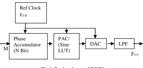
The resolution of a DAC is specified by the number of input bits. For example, the resolution of a DAC with 10 input bits is referred to as having 10 bit resolution. The impact of DAC resolution is most realized by the sine wave reconstruction. The deviation between a DAC output signal and a perfect sine wave leads to the error introduced as a result of its finite resolution. This error is the quantization error that gives rise to the quantization distortion. The sharp edges in the DAC output signal imply the presence of high frequency components superimposed on the fundamental. It is the high frequency components that constitute quantization distortion. In the frequency domain, quantization distortion errors are aliased within the Nyquist band and appear as discrete spurs in the DAC output spectrum. As the DAC resolution increases the quantization distortion decreases; i.e., the spurious content of the DAC output spectrum decreases. Thus, an increase in resolution Phase
Accumulator (N Bit)
PAC/ (Sine LUT)
[image:2.612.55.302.105.224.2]LPF DAC
Fig.1. Basic scheme of DDFS
M
Ref Clock fCLK
3.
PROPOSED DDFS DESIGN
SIMULATION
In the proposed work, DDFS has been designed and simulated using Matlab and Xilinx AccelDSP tool by making an efficient realization of Slices & LUT’s available on the target FPGA. The design details of the proposed DDFS design include the DDS operating frequency value of 100 MHz i.e. the frequency at which DDFS will operate, with the required frequency. resolution of 100 Hz and accumulator size of 20 bits. The first step is the development of m code with the required specifications [9] following the verifying of the floating point which reads and analyzes a MATLAB floating point design.
In a later pass, through this flow, the design directives can be added for finding the best hardware architecture of the design. The AccelDSP tool reads and analyzes a MATLAB floating-point design and invokes a MATLAB simulation to verify the fixed-point design. The design flow [10] is shown in Fig. 2.
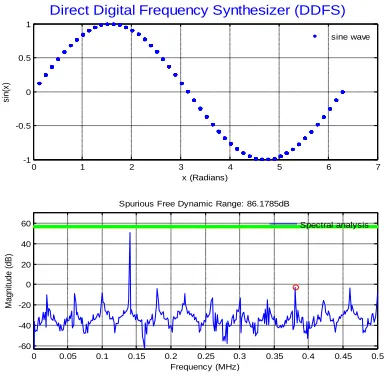
The fixed point model is generated and then to verify the match the Fixed-Point Plot & the Floating-Point Plot are compared. The equivalent fixed point file is developed & verified and should match to the closet with the floating point design in step 2. The fixed point design is shown in the Fig. 3. The sine wave is being generated through the DDFS whose FFT analysis illustrates the spurious performance of the proposed DDFS design. The spectral purity of the design is 86.17dB. The measured spectrum plot shows a red indication in the plot which illustrates the largest harmonically related unwanted spur in the spectrum. The DDFS fits perfectly for SDR in modern FPGA integrated with embedded multipliers & LUT’s & allows reaching high Speed & SFDR.
4.
HARDWARE SYNTHESIS RESULTS &
DISCUSSIONS
[image:3.612.66.258.216.406.2]To observe the Speed & hardware utilization, RTL is developed and verified & then synthesized to the gate level netlist to be implemented on Spartan 3E based XC3S500E and Virtex 2 Pro based XC2VP307FF896 FPGA target device which is operated at an estimated frequency of 116.2 MHz and 146.5 MHz respectively. The optimized resource utilization of both the devices is shown in Table 1.
Table 1. Implementation results for optimized DDFS
Implementation Spartan 3e Virtex 2p
# of Slices 81 of 4656 87 of 13696
# of Flip Flops 105 of 9312 105 of 27392
# of 4 input LUTs 140 of 9312 150 of 27392
Estimated Frequency 116.2 MHz 146.5 MHz
Estimated Period 8.6050 ns 6.8240 ns
SFDR upto fclk/2^n 86.17dB 86.17dB
The proposed DDFS design is compared with the existing work based on Spartan 3 based XC3S400-4FT256 and Virtex 2P based XC VP30-7FF896 device. Table 2 shows the performance comparison of the proposed DDFS design with similar architecture of existing work implemented on Spartan 3 and Virtex 2P based target FPGAs. Spartan 3E, used in the hardware simulation is more cost effective than virtex 2P, which shows an efficient resource utilization in terms of Slice Flip Flops and the number of 4-input LUT’s is less as compared to the existing results on Virtex 2P target device. Spartan series devices thus achieve high performance, low cost operation through the use of anadvanced architecture and semiconductor technology.
Direct Digital Frequency Synthesizer (DDFS)
0 1 2 3 4 5 6 7
-1 -0.5 0 0.5 1
x (Radians)
s
in
(x
)
sine wave
0 0.05 0.1 0.15 0.2 0.25 0.3 0.35 0.4 0.45 0.5
-60 -40 -20 0 20 40 60
Spurious Free Dynamic Range: 86.1785dB
Frequency (MHz)
M
a
g
n
it
u
d
e
(
d
B
)
Spectral analysis
Fig.3. FFT fixed point design
1 Project
2 Verify Floating Point
3 Analyze
4 Generate Fixed Point
5 Verify Fixed Point
8 Synthesize RTL
6 Generate
RTL 9 Implement
[image:3.612.316.564.337.519.2]7 Verify RTL
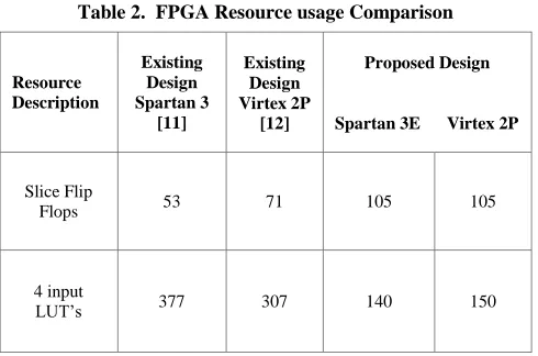
[image:3.612.44.305.501.659.2]Table 2. FPGA Resource usage Comparison
Resource Description
Existing Design Spartan 3
[11]
Existing Design Virtex 2P
[12]
Proposed Design
Spartan 3E Virtex 2P
Slice Flip
Flops 53 71 105 105
4 input
LUT’s 377 307 140 150
[image:4.612.48.296.421.511.2]The Spartan series targets applications with low power footprint, extreme cost sensitivity and high volume. Virtex has high performance feature and capacity whereas Spartan for low cost and power consumption. Each logic block in an FPGA typically has small number of inputs and outputs . The Spartan and Virtex family also features different types of logic blocks. The most commonly used logic block is a Lookup table, which contains logic cells used to implement the small logic function.Thus, in order to fill the existing gaps in today’s wireless communication techniques, the design utilizing optimal number of resources on FPGA device has been developed which provides a cost effective solution for SDR applications. The results shows that the proposed design is consuming considerably less resources in terms of LUTs and provides an enhanced estimated period of 6.8240 ns and SFDR of 86.17dB.
Table 3. Performance Comparison Table
Specificat-ions
[13] ASIC
[14] ASIC
[15] FPGA
Proposed Design
Fclk(MHz) 88 150 43.3 146.5
SFDR(dBc) -80 -84 -88 -86.17
Table 3 shows the performance of DDFS design in terms of Speed and SFDR as compared to the ASIC implementation. The proposed design that has been synthesized can be implemented on arbitrary technologies. The result shows a considerable improvement with the operating frequency for optimizing the Speed & SFDR in the proposed design based on FPGA which allows faster implementation, flexibility & reconfigurability.
5.
CONCLUSION
In this paper, an efficient method is presented with proposed DDFS design which supports low hardware requirements in terms of LUT’s available on FPGA target device. The proposed design is consuming 81 slices, 105 flip flops and 140 LUTs of Spartan 3 FPGA and consuming 150 LUTs of Virtex 2P FPGA device. The developed DDFS can operate at an estimated frequency of 146.5 MHz. The SFDR of 86.17 dB can be
appropriate to provide cost effective and high performance solution for SDR based wireless application.
6.
REFERENCES
[1] Shiann-Shiun Jeng, Hsing-Chen Lin, Chen-Yu Wu “DDFS Design Using the Equi-Section Division Method for SDR Transceiver” IEEE 19th International Symposium on Personal, Indoor and Mobile Radio Communications, pp.1 – 5, 2008.
[2] Yasir A. Khan, Anees Ullah, Hazrat Ali, Khwaja M. Yahya, Nazim Ali, “Differential Based Area Efficient ROM-Less Quadrature Direct Digital Frequency Synthesis” IEEE International Conference on Emerging Technologies ICET, pp.81 – 86, 2009.
[3] Indranil Hatai and Indrajit Chakrabarti “A High-Speed, ROM-Less DDFS for Software Defined Radio System” in IEEE journal of Solid-State Circuits, Vol.45, No.11, pp. 115 – 119, November 2010.
[4] Indranil Hatai and Indrajit Chakrabarti “A Novel Low-Latency, High-Speed DDFS Architecture” in IEEE Annual India Conference (INDICON), pp. 1 – 4, 2010.
[5] Y. H. Chye, M. F. Ain, Norzihan M. Zawawi “Design of BPSK Transmitter Using FPGA with DAC” IEEE 9th Malaysia International Conference on Communications (MICC), pp. 451 – 456, December 2009.
[6] Tierney, C Rader, B. Gold, "A digital frequency synthesizer", IEEE Transaction on Audio and Electro acoustics, Vol. 19, No. 1, pp. 48-57, March 1971.
[7] Analog Devices, A technical tutorial on digital signal synthesis,1999.
http://www.analog.com/static/importedfiles/tutorials/45096 8421DDS_Tutorial_rev12-2-99.pdf.
[8] Khilar S., Kiran Parmar, Saumi S., Dasgupta K.S. “Design and Analysis of Direct Digital Frequency Synthesizer” IEEE International Conference on Emerging Trends in Engineering & Technology, pp.1302 – 1306, 2008.
[9] Rajesh Mehra and Swapna Devi “FPGA implementation of High Speed Pulse Shaping Filter for SDR Applications” SpringerLink Recent Trends in Networks and Communications in Computer and Information Science, Vol. 90, Part 1, pp. 214-222, 2010.
[10]AccelDSP Synthesis Tool User guide manual, Xilinx Release 10.1, March, 2008.
[11]Muhammad Asim Butt and Shahid Masud “FPGA based Bandwidth adjustable All Digital Direct Frequency Synthesizer” IEEE International Symposium on Communications and Information Technology, pp. 1399 – 1404, 2009.
[12]Omran H., Sharaf K., Ibrahim M. “An All-Digital Direct Digital Synthesizer Fully Implemented on FPGA” IEEE 4th International Design and Test Workshop (IDT), pp.1-6, 2009.
in IEEE Custom Integrated Circuits Conference Paper, pp.163–166, October 2004.
[14]J. M. P. Langlois, and D. Al-Khalili, “A Low Power Direct Digital Frequency Synthesizers in 0.18-mμ CMOS,” in IEEE Custom Integrated Circuits Conference Paper, pp.283–286, September 2003.
[15]G. Bouzid, H. Trabelsi, Z. Elabed, M. Masmoudi “FPGA Implementation of FHSS-FSK Modulator” in IEEE International Conference on Design & Technology of Integrated Systems in Nanoscale Era, pp.1 – 5, 2008.
7.
AUTHORS PROFILE
Bindiya Kamboj: Mrs. Bindiya Kamboj is currently pursuing
Master of Engineering from National Institute of Technical Teachers’ Training & Research, Chandigarh, India. She has completed her B.Tech in Electronics & Communication
Engineering from D.I.E.T, Karnal, Kurukshetra University, Haryana in 2007. Her areas of interests are Digital Signal Processing, VLSI Design, Embedded System Design.
Rajesh Mehra: Mr. Rajesh Mehra is currently Assistant