Compositional Plane of a New Wide-Gap Solid Solution Semiconductor
CaPbSeS and Epitaxial Thin Film Growth of CaSe
Seishi Abe and Katashi Masumoto
The Research Institute for Electric and Magnetic Materials, Sendai 982-0807, Japan
We have systematically investigated the compositional plane of solubility range and lattice constants in Ca1xPbxSe1ySysystem, and as a
first step for preparation of the ternary system, we have also investigated the growth and characterization of the CaSe thin films.
Solubility range and lattice constant of a Ca1xPbxSe1ySysystem was investigated using powder synthesis under thermal equilibrium
condition. A CaSe thin film was grown on a cleaved BaF2(111) substrate by means of a hot-wall epitaxy.
The solubility limit at 1273 K varies with respect to the Se concentrationy, taking a minimum limit of 0.04 aty¼0:8and a maximum of 0.24 aty¼0. It is found that the system can be lattice-matched to PbS and InP. The CaSe thin films are grown epitaxially at substrate temperature range between 673 and 873 K. The energy band gap of the film is estimated to be 4.62 eV at RT through measurement of transmittance and reflectance of the film, having full-width at half-maximum (FWHM) of X-ray rocking curve of 0.08by!{2scan at (222) Bragg reflection.
(Received March 22, 2005; Accepted June 6, 2005; Published September 15, 2005)
Keywords: solid solutions, calcium compounds, semiconducting II–VI materials, heterojunction semiconductor devices, hot-wall epitaxy, compositional plane, epitaxial thin film growth
1. Introduction
Novel devices such as quantum cascade laser and optical switch can be operated through intersubband transition of electron in superlattice structure, which is made of alternated layers of semiconductors with different energy band gaps. Enlargement of the conduction band offset in heterojunction allows to shorten the wavelength of the emitted light toward near-infrared region for quantum cascade laser, and to apply the optical switch as an advanced device in the optical communication system at around 1.55mmused practically.
Up to now, many studies for the layered semiconductors with different energy band gaps have been carried out on AlN/GaN,1) AlAs/InGaAs,2) AlAsSb/InGaAs3) and BeTe/ ZnSe.4)In addition to the consideration of band alignment, lattice-match condition between such heterostructure and substrate is also important, since the large lattice mismatch between AlAs and InP substrate in the AlAs/InGaAs system, for example, either limits the number of quantum wells that can be grown without significant material degradation or requires a novel growth technique of growing a linearly graded composition buffer layer to accommodate the strain.2) Accordingly, AlAsSb/InGaAs heterostructure can only be lattice-matched to substrate among these systems, bringing conduction band offset of 1.75 eV5,6) under type II band alignment in spite of energy band gap difference of 1.8 eV between the two systems.
In order to shorten the intersubband transition wavelength toward visible region, other materials with larger conduction band offset should be designed under keeping lattice-matched condition. As another possible candidate for such materials, we propose a new wide-gap solid solution of Ca1xPbxSe1ySy system. This system is characterized with
the combination of wide gap calcium chalcogenide systems of Ca1xPbxSe1ySy and narrow gap lead chalcogenide
systems of Pb1x0Cax0S1y0Sey0. The latter system has been
found for a mid-infrared laser in our previous study.7)It is
expected in the proposed system that there is a considerable large difference in the energy band gap between the two systems, and that its layered structure is lattice-matched to substrate. As a result of the design of the new material, Ca1xPbxSe1ySy system has potential to bring larger
conduction band offset compared to the AlAsSb/InGaAs heterostructure among the lattice-matching systems, thanks to these materials combination of wider- and narrower-semiconductors in energy band gap.
The main advantage of CaSe in the alkaline-earth selenide compounds is followed that CaSe is predicated to be direct band-gap material since the valence-band maximum occurs at the point whereas the minimum in conduction band at the X point for MgSe, at thepoint for CaSe, and at the K point for SrSe.8)
The fundamental problem may be difficulty to predict the properties of the solid solution Ca1xPbxSe1ySyat a given
composition x and y, since a mixed crystal often has a miscibility gap. And besides, the compositional plane of the system will be valuable to design each of the layers in the lattice-matched hetero-structure. On the other hand, a method to prepare ternary or quaternary thin films must be developed in order to fabricate hetero-epitaxial superlattice structure employing the Ca1xPbxSe1ySysystem. However, even the
binary CaSe epitaxial thin film has not been fabricated yet, and also, the energy band gap at RT of CaSe is not still clear. Therefore, in the present study, we have systematically investigated the compositional plane of solubility range and lattice constants in Ca1xPbxSe1ySy system using powder
synthesis, and as a first step for preparation of the ternary system, we have also investigated the growth and character-ization of the CaSe thin films using hot-wall epitaxy method.
2. Experimental Procedure
Solubility range and lattice constant of a Ca1xPbxSe1ySy
system was investigated using powder synthesis under Special Issue on Narrow and Wide-Bandgap Semiconductor Materials
thermally equilibrium condition. The elements used were CaSe (99.5%), CaS (4N), PbS and PbSe, and they were weighed for a desired composition of Ca1xPbxSe1ySy, and
mixed in an agate mortar. Then, the mixed powder was heat-treated at 1273 K for 48 h in order to obtain a thermal equilibrium state. The above-mentioned PbS and PbSe compounds were synthesized from the elements having 6N purity. The lattice constants of the Ca1xPbxSe1ySysystem
thus obtained were determined by powder X-ray diffraction with Cu K radiation, and then the solubility range was estimated.
A CaSe thin film was grown on cleaved BaF2(111)
substrates by means of a hot-wall epitaxy (Fig. 1). The choice of BaF2 substrate was motivated by its ultraviolet–visible
transparency, negligible vapor pressure at a grown temper-ature employed and relatively near lattice constant for CaSe compared to other substrate. The apparatus used consists of four electric furnaces, which are for substrate, wall, source and reservoir, as shown in the figure, and can be controlled independently in temperature. Ca (99.5%) is used as the source material, and Se (6N pure) is used as the reservoir material. Each of the vaporized elements would react on the substrate to form CaSe compound.
Before the growth of CaSe thin film, Ca was preheated at a source temperature (Tsou) of 843 K for 30 min in order to stabilize the Ca vapor flux through the growth run. Wall temperature in the apparatus was kept constant at 823 K through the present study.
Growth orientation of the films was determined by high-resolution X-ray diffraction (XRD) with a four-crystal monochromator. Thickness of the films was measured by a surface texture analysis system. Spectral transmittance and reflectance at RT of the films were observed at the wave-length range from 600 to 200 nm by UV/VIS and NIR measurement.
3. Results and Discussions
Figure 2 shows the typical powder X-ray diffraction patterns of the Ca1xPbxSe1ySysolid solution system (y¼
0). As seen in the figure, a single phase in the Ca1xPbxSe
system is observed on the concentration range belowx¼0:1, which can be characterized with NaCl structure, while two phases consisting of Ca rich Ca1xPbxSe compound and Pb
rich Pb1x0Cax0Se compound are observed atx¼0:4.
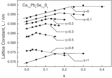
Figure 3 shows the lattice constants of various Ca1x
-PbxSe1ySysystem as a function ofxat the fixed composition
y, where the results of the Ca rich region are represented. A lattice constant of the Ca1xPbxSe1ySysystem shown in the
figure were determined by linear extrapolation to zero of the values derived through the Nelson-Riley function9) employ-ing the Bragg peaks above 2¼100. The solid line
indicates the single-phase region, and the dotted line indicates the two phases region, in which the lattice constants of the Ca rich compound are presented. As can be seen in the figure, the lattice constants increase linearly in proportion tox
within the solubility range, irrespective of the concentration
y. The on-setting compositionxto deviate from the linearity according to Vegard’s law10) is always regarded as the solubility limit. In the two phases region, on the other hand, the lattice constants at y¼0 and 1.0 seems to be almost constant with respect to xin contrast to decrease in lattice constant with increasingxfor other concentrations y. These different variations of the lattice constants in the two phases region is attributed to difference in the number of degree of freedom in the Ca1xPbxSe1ySysystem according to Gibbs’
phase rule. Namely, in case of solid-solid reaction, the number of degrees of freedom must be specified to completely describe the state of the system at y¼0 and 1.0 when the temperature of heat-treatment is kept constant at 1273 K because of the component of 2 in the ternary system, reservoir material
source materials quartz liner
substrate heater
thermocouple
SUBSTRATE : BaF2
WALL
SOURCE : Ca
RESERVOIR : Se
Fig. 1 Schematic representation of the hot-wall epitaxy apparatus used for the fabrication of CaSe thin films.
20° 40° 60° 80°
0 200 400 600 800 1000 1200
1400 Ca1-xPbxSe
PbCaSe
x=0
x=0.05
x=0.10
(422)
(420)
(331)
(400)
(222)
(311)
(220)
(200)
(111)
x=0.40
Intensity (arb. unit)
2θ
Fig. 2 Typical powder X-ray diffraction patterns of the Ca1xPbxSe1ySy
(y¼0) solid solution system.
0.0 0.1 0.2 0.3 0.4
0.570 0.575 0.580 0.585 0.590 0.595 0.600
y=0
y=0.1
y=0.2
y=0.3
y=0.5
y=0.8
y=1
Ca1-xPbxSe1-ySy
Lattice Constant,
L
/ nm
x
[image:2.595.334.517.73.201.2] [image:2.595.76.262.75.242.2] [image:2.595.333.519.258.388.2]while the number in the other concentrationsyis not specified even though the temperature is kept constant because of the component of 3 in the quaternary system.
Table 1 shows the compositional dependence of the lattice constant within the solubility range at the fixed composition
y. There can be seen the positive inclination of the lattice constant with respect to x in all cases, and also seen the tendency to decrease in the section of the lattice constant at
x¼0with decreasingy. The facts that the addition of PbSe to CaSe causes the increase of the lattice constant, while the addition of CaS to CaSe causes its decrease are obviously due to the differences in the ionic radii between Ca and Pb and between Se and S, respectively.
Figure 4 shows the solubility range and lattice constant of the Ca1xPbxSe1ySy system. The dashed line indicates the
isolattice-matched line, and the solid line indicates the solubility limit at 1273 K obtained from the variation of the lattice constants (Fig. 3). The relations of lattice-matched to PbS and InP are also represented by the dotted line in the same figure. The solubility limit at 1273 K varies with respect to the Se concentrationy, being resulted in minimum limit of 0.04 at y¼0:8 in contrast to a maximum limit of 0.24 at
y¼0. From the results shown in Figs. 3 and 4, it is seen that the lattice constant of the Ca1xPbxSe1ySy system varies
continuously from 0.5696 (CaS) nm to 0.5993 nm (Ca0:76Pb0:24Se), and it is clear that the Ca1xPbxSe1ySy
system can be lattice-matched to PbS and InP, which will be employed as substrate in order to fabricate the devices operated through intersubband transition.
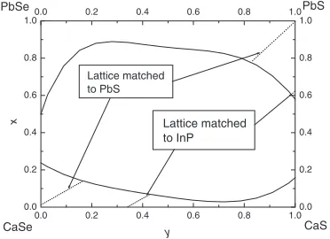
Figure 5 shows the relationship of the solubility limits in the Ca1xPbxSe1ySysystem with respect to the constituent
elements of PbSe, PbS, CaSe and CaS, by combining the present result for Ca rich region and the previous result for Pb rich region.7)The relation of lattice-matched to PbS and InP is also shown with the dotted lines. It is seen from the figure that the isolattice-matched lines to PbS and InP exist in both Pb rich region (upper part in the figure) and Ca rich region (lower part), respectively. This implies that a lattice-matched heterostructure constructed by layering alternately Ca rich wide-gap compound and Pb rich narrow-gap compound is expected to give rise to a large difference in energy band gap. A numerical estimation of the difference will be performed in the following section, since the energy band gap at RT of CaSe has not only been reported yet among these constituent elements.
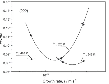
[image:3.595.61.271.97.367.2]Next, we shall investigate CaSe thin films as a first step for preparing the quaternary thin films. Figure 6 shows the growth rate of the CaSe thin films as a function of inverse of the source temperature (Tsou) under the reservoir temperature (Tr) of 498, 523 and 543 K. The substrate temperature (Tsub) was kept constant at 873 K. The plots of and mean detection and no detection of XRD peaks respectively within the precision of our experimental technique. The films with no detection of XRD peaks has brown-colored appearance in contrast to the colorless appearance in other films, indicating no sign of surface degradation for storage in ambient air. As can be seen in the figure, CaSe films with no XRD peaks Table 1 Lattice constants in the solubility range as a function of xfor
Ca1xPbxSe1ySy.
y Lattice constant
(nm)
1 0:5696þ0:0314x x0:16
0.8 0:5757þ0:0213x x0:04
0.5 0:5832þ0:0366x x0:05
0.3 0:5876þ0:0235x x0:10
0.2 0:5900þ0:0234x x0:12
0.1 0:5914þ0:0252x x0:18
0 0:5933þ0:0249x x0:24
0.0 0.2 0.4 0.6 0.8 1.0
0.00 0.05 0.10 0.15 0.20 0.25
Ca1-xPbxSe1-ySy
0.595 nm
0.573 nm
0.590 nm
Lattice matched to InP Lattice matched to PbS
Solubility limit at 1273 K
x
y
Fig. 4 Solubility range and lattice constant of the Ca1xPbxSe1ySy
system.
0.0 0.2 0.4 0.6 0.8 1.0
0.0 0.2 0.4 0.6 0.8
1.00.0 0.2 0.4 0.6 0.8 1.0
0.0 0.2 0.4 0.6 0.8 1.0
Lattice matched to InP Lattice matched to PbS
PbSe PbS
CaS CaSe
x
y
Fig. 5 Relationships of solubility limits in Ca1xPbxSe1ySysystem with
respect to the constituent elements of PbSe, PbS, CaSe and CaS. The data in Pb rich region has been referred from our previous result.7) Relation-ships of lattice-matched to PbS and InP are also shown.
1.14 1.16 1.18 1.20 1.22 1.24 1.26 1.28 1.30 1.32 10-10
no detection of XRD peaks
T r :498 K T
r :523 K T
r :543 K
Growth Rate, r / m s
-1
Tsou-1 / 10-3
K-1
[image:3.595.79.261.227.367.2] [image:3.595.333.519.283.425.2]seems to be appeared at the relatively lowTr of 498 K. It is responsible for the fact that the Se vapor flux from the reservoir might be insufficient so as to construct well diffracting CaSe compound, suggesting considerable devia-tion from the appropriate ratio of Se/Ca vapor flux. The growth rate clearly depends on the Tsou, so that growth process of the CaSe thin films is limited by the sublimation of Ca resource, being estimated activation energy to be 113 kJ/ mol atTr of 523 K assuming linear variation. It is also clear from the figure that the amount of Ca deposited on the substrate would be decreased with increasing the Se vapor flux when the Tsou will be kept constant, since the linear variation of the growth rate shifts toward higher Tsou as increasingTr. Accordingly, it is found that the vaporization from Ca resource is strongly affected by that from Se resource in the hot-wall epitaxy method.
Figure 7 shows the full-width at half-maximum (FWHM) of X-ray rocking curve by!{2scan at (222) as a function of the growth rate. As seen in the figure, the FWHM seems to be varied parabolically with respect to the growth rate, being caused by change in vapor flux ratio of Se/Ca. Namely, atTr of 523 K, for example, FWHM comes to a minimum in the vicinity of1:271010m s1, meaning that an appropriate
vapor flux ratio of Se/Ca is realized at the growth rate, while a growth rate higher than 1:271010m s1 brings Ca
excess deviation from the appropriate ratio, and a lower growth rate leads to Se excess deviation. The appropriate ratio, however, cannot be evaluated numerically in the present study because of no monitoring system of these vapor fluxes in the apparatus used. The parabolic variation shift toward higher growth rate as increasing theTr, and, atTrof 543 K, the CaSe thin film has the FWHM of 0.08 by!{2
scan and 0.29 by ! scan, which is the best crystallinity
obtained in the present study. A FWHM of the diffractogram obtained by!scan reflects a degree of mosaicity of a crystal in contrast to unevenness of the lattice constant by!{2scan. Therefore, the quality of the CaSe thin films is limited by mosaicity rather than unevenness of lattice constant. The considerable large FWHM by ! scan compared to that by !{2 scan would be attributed to lattice misfit of 4.45% between CaSe and BaF2 substrate.
Figure 8 shows typical XRD pattern of CaSe thin films at
Tsubof 873 K by!{2scan (a) and-scan (b). As can be seen
in the patterns (a) that (111) and (222) peaks of CaSe thin film with NaCl structure are observed together with the peaks of BaF2 substrate, taking the growth orientation at [111]
direction on cleaved BaF2(111) substrate. Similar patterns
have been observed on the thin films grown at theTsubrange from 673 to 873 K. We also investigated the in-plane texture of the film by azimuthal -scan (b). Every 120 of these
reflections confirm that the film contains a single cubic texture in the film plane. Therefore, epitaxial growth of the CaSe thin film can be successfully performed employing the hot-wall epitaxy. Moreover, FWHM of the X-ray rocking curve at (222) by ! scan decreased monotonically with increasing theTsub. Thus, crystallinity of the CaSe thin films can be improved with respect to theTsub.
So far, optical absorption at 77 K of CaSe thin films deposited on quartz plate11)and optical reflectivity at 2 K of CaSe single crystal12)have been reported, observing several energy peaks of 4.87 and 5.11 eV in the former, and of 4.828, 5.056 and 5.60 eV in the latter. Optical energy band gap, however, have not been estimated experimentally through optical absorption coefficient. Then, we have tried to estimate the energy band gap at RT of the CaSe thin film grown epitaxially. Figure 9 shows the typical absorption edge at RT of the CaSe thin film grown at the Tsub of 873 K. The absorption coefficient of the CaSe thin film was obtained through the measurement of transmittance and reflectance of the film, employing the following expression: d¼
lnðTobs1Þ þlnð1RobsÞ þlnð1R0obsÞ þlnð1R
0
obsþRsobs=
10-10 0.07°
0.08° 0.09° 0.10° 0.11° 0.12° 0.13° 0.14° 0.15°
(222)
Tr : 498 K
FWHM
Growth rate, r / m s-1 Tr : 523 K
Tr : 543 K
Fig. 7 The full-width at half maximum (FWHM) of X-ray rocking curve by!{2scan as a function of growth rate.
20° 30° 40° 50° 60°
0 2000 4000 6000
CaSe (222)
CaSe (111) BaF
2
(222)
BaF
2
(111)
Tsub:873 K
Intensity (arb. unit)
2θ
φ
-150° -100° -50° 0° 50° 100° 150°
100 200 300 400
(422)
Intensity (arb.unit)
(b)
(a)
Fig. 8 Typical XRD pattern of CaSe thin films atTsubof 873 K by!{2 scan (a) and-scan (b).
4.0 4.2 4.4 4.6 4.8 5.0
0.0 5.0x10¹⁰
1.0x10¹¹
1.5x10¹¹
2.0x10¹¹
2.5x10¹¹
3.0x10¹¹
(
α
·h
ω
)
–
2/ eV 2cm
-2
at RT
Photon energy, E / eV
[image:4.595.79.266.74.217.2] [image:4.595.337.517.77.223.2] [image:4.595.334.519.283.411.2]2Þ,13) where d is the thickness of the film, Tobs is trans-mittance,Robsis reflectance observed at film-side andR0obsis reflectance observed at substrate-side. So that, the energy band gap is estimated to be 4.62 eV by linear extrapolation to zero of theh!squared. In addition, no energy peaks are observed at the photon energy range above the optical absorption edge.
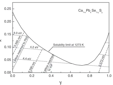
Figure 10 shows x{y compositional plane of the Ca1xPbxSe1ySysystem. The isoenergy band gap lines with
respect to the compositions in Ca1xPbxSe1ySy system are
estimated using the following expressions: Eg¼4:62
4:21x0:12y0:02xy, where linear variation of the energy band gap between the constituent elements is assumed as first-approximation, employing 4.62 eV for CaSe, 4.5 eV for CaS,14)0.27 eV for PbSe15)and 0.41 eV for PbS.15)As a result of obtaining the energy band gap of CaSe, relation between lattice constant and energy band gap of Ca1xPbxSe1ySy
system can be discussed. In general, energy band gap of ternary- or quaternary-system with miscibility gap varies nonlinearly with respect to composition. In the present study, it is anticipated that Ca1xPbxSe1ySy system has also
nonlinear variation of energy band gap with respect to Pb content. It is found from the figure that there can be considered Ca0:99Pb0:01Se/PbS- or CaSe0:66S0:34
/InP-hetero-structure, for example, in case of employing ternary compound. We can see that large band gap difference of about 4 or 3 eV is possibly obtained in Ca0:99Pb0:01Se/PbS or
CaSe0:66S0:34/InP. We should pay attention to the
substan-tially large difference in energy band gap under keeping lattice-match condition with the substrate, suggesting the Ca1xPbxSe1ySy system to have considerable promise as a
material for devices through intersubband transition. We need further investigations concerning the bowing parameter in the variation of energy band gap and the type of band alignment in these heterostructure through preparation of ternary or quaternary thin film growth.
4. Conclusion
It may be remarked that the Ca1xPbxSe1ySy system is
regarded as good candidate materials for producing com-pounds to construct the devices to be operated through intersubband transition. Ca1xPbxSe1ySy system has
ade-quate solubility limit at 1273 K to form such solid solution semiconductor, being lattice-matched to PbS and InP used as substrate. It would be also pointed out that epitaxial growth of CaSe thin films are successfully performed through the
Tsub range between 673 and 873 K by means of hot-wall epitaxy. The energy band gap of the CaSe is found to be 4.62 eV at RT optical absorption spectrum. Based on the results obtained in the present study, ternary and quaternary CaSe-based solid solution thin films will be fabricated in our subsequent investigation, expecting to bring advanced optical devices.
REFERENCES
1) C. Gmachi, H. M. Ng, S.-N. G. Chu and A. y. Cho: Appl. Phys. Lett.77 (2000) 3722–3724.
2) B. Sung, H. C. Chui, M. N. Fejer and J. S. Harris, Jr.: Electron. Lett.33 (1997) 818–820.
3) T. Mozume, H. Yoshida, A. Neogi and M. Kudo: Jpn. J. Appl. Phys.38 (1999) 1286–1289.
4) R. Akimoto, Y. Kinpara, K. Akita, F. Sasaki and S. Kobayashi: Appl. Phys. Lett.78(2001) 580–582.
5) Y. Nakata, Y. Sugiyama, T. Inata, O. Ueda, S. Sasa, S. Muto and T. Fujii: MRS Symp. Proc.198(1990) 289–294.
6) 1eV¼1:602181019J
7) S. Abe and K. Masumoto: J. Crystal Growth204(1999) 115–121. 8) R. Pandey, J. E. Jaffe and B. Kunz: Phys. Rev. B43(1991) 9228–9237. 9) J. B. Nelson and D. P. Riley: Proc. Phys. Soc.57(1945) 160–177. 10) L. Vegard: Z. Phys.5(1921) 17–26.
11) G. A. Saum and E. B. Hensley: Phys. Rev.115(1959) 1019–1022. 12) Y. Kaneko and T. Koda: J. Crystal Growth86(1988) 72–78. 13) S. Yoshida and H. Yajima:Optical thin films and devices, (Univ. of
Tokyo Press, Tokyo, 1994) pp. 73.
14) N. Yamashita: Jpn. J. Appl. Phys.30(1991) 1384–1485.
15) J. N. Zemel, J. D. Jensen and R. B. Schoolar: Phys. Rev.140(1965) A330–A342.
0.0 0.2 0.4 0.6 0.8 1.0
0.00 0.05 0.10 0.15 0.20 0.25
4.2 eV
4.4 eV 4.0 eV
Ca1-xPbxSe1-ySy
0.595 nm
0.573 nm
0.590 nm Lattice ma tched
to InP Lattice ma
tched to PbS
Solubility limit at 1273 K
x
[image:5.595.81.263.70.208.2]y