Timing-Driven Variation-Aware Partitioning and
Optimization of Mixed Static-Dynamic CMOS Circuits
Kumar Yelamarthi
School of Engineering and Technology, Central Michigan University, Mt Pleasant, USA Email: [email protected]
Received August 20, 2012; revised November 6, 2012; accepted November 13, 2012
Copyright © 2013 Kumar Yelamarthi. This is an open access article distributed under the Creative Commons Attribution License, which permits unrestricted use, distribution, and reproduction in any medium, provided the original work is properly cited.
ABSTRACT
The advancement in CMOS technology has surpassed the progress in computer aided design tools, creating an avenue for new design optimization flows. This paper presents a design level transistor sizing based timing optimization algo- rithms for mixed-static-dynamic CMOS logic designs. This optimization algorithm performs timing optimization through partitioning a design into static and dynamic circuits based on timing critical paths, and is further extended through a process variation aware circuit level timing optimization algorithm for dynamic CMOS circuits. Implemented on a 64-b adder and ISCAS benchmark circuits for mixed-static-dynamic CMOS, the design level optimization algo- rithm demonstrated a critical path delay improvement of over 52% in comparison with static CMOS implementation by state-of-the-art commercial optimization tools.
Keywords: Timing Optimization; Dynamic CMOS Circuits; Process Variations; Delay Uncertainty
1. Introduction
The advancement in CMOS technology has created an avenue for several new initiatives, while at the same time has also presented challenges such as timing uncertainty
max min , where Tmax and Tmin are maximum and
minimum delays from process variations, timing closure, reliability and leakage current. At 180 nm CMOS tech- nology, process variations have caused about 30% varia- tion in chip frequency, along with 20× variation in chip leakage [1]. This magnitude of process variations is pre- dicted to increase and cause detrimental effects as CMOS technology is transitioning to 22 nm. For instance, the magnitude of intra-die channel length variations have been estimated to increase from 35% of total variation in 130 nm, to 60% in 70 nm CMOS technology; and varia- tion in wire width, height, and thickness is also expected to increase from 25% to 35% [2], highlighting the re- quirement for new and efficient timing optimization me- thods.
T T
Significant literature exists on transistor sizing [3-6], but most existing transistor sizing algorithms focus to- wards static CMOS circuits and technologies using dual threshold voltages. TILOS [4] presented an algorithm used for iteratively sizing transistors by a factor in the critical path. However, this algorithm does not guarantee a convergence of timing optimization and is not a deter-
ministic approach. MINFLOTRANSIT [5] is an algo- rithm proposed for transistor sizing based on iterative re- laxation method but requires generation of directed acy- clic graphs iteratively for timing optimization.
Several methods to reduce the effect of process varia- tions were presented in [1,7-10]. These methods deal with statistical variations and are not optimal for designs with large number of parameter variations. The Adaptive Body Biasing (ABB) technique presented in [1,9] is im- plemented on post-silicon designs where each die re- ceives a unique bias voltage thus reducing uncertainty of the frequency variation. However, it is not feasible for addressing intra-die variations, as each block in the de- sign requires a unique bias voltage. Another limitation using this method is the increased leakage power due to reduction in the threshold voltage. A keeper based method was presented in [10] for designs with large number of parallel stacks similar to NOR gates, but is not optimal for designs without parallel stacks as it requires addi- tional hardware to program the keepers.
overall capacitance and aids towards increasing the tim- ing performance compared to its static CMOS counter- part. This advantage comes at the cost of power con- sumption, and increased complexity in transistor sizing due to charge sharing, noise-immunity, and sensitivity to process variations. With static and dynamic circuits hav- ing their unique advantages, using both the circuit styles efficiently results in superior design performance. Tim- ing constraints can be met through optimizing the critical path delay at the cost of increasing delay in non-critical paths. Based on these properties and our previous work [11,12], this paper presents a design level timing optimi- zation flow for mixed-static-dynamic CMOS logic. This algorithm performs timing optimization by finding the timing critical paths in the design, substituting them with performance optimized custom dynamic CMOS circuits, to result in an effective balance of power, timing, and area. One of the unique advantages of the proposed algo- rithm is its ability to embed into the existing optimization flows for easy adaptability.
This paper is organized as follows. Section 2 intro- duces dynamic CMOS circuit logic and a new circuit level optimization (CLO) algorithm for optimization of worst-case delay, delay uncertainty, and delay sensitivity. Validation of the proposed CLO algorithm is presented in Section 3 through implementation on several ISCAS benchmark circuits. Further, based on the circuit level timing optimization algorithm, a design level optimiza- tion algorithm for mixed-static-dynamic CMOS logic cir- cuits is presented in Section 4, and validation through implantation on ISCAS benchmark circuits is presented in Section 5. Finally, conclusion is presented in Section 6.
2. Circuit Level Optimization
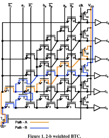
The delay of dynamic CMOS circuits is highly depend- ent on the number and size of transistors on the critical path. Increasing transistor sizes in a critical path in- creases the discharging current, thus reducing path delay. However, increasing transistor sizes to reduce delay in- creases load capacitance of channel-connected transistors on other paths and also their respective delays. Consider a 2-b Weighted Binary-to-Thermometric Converter (WBTC) as shown in Figure 1 with two timing paths: path-A and path-B highlighted. An experiment of opti- mizing path-A was performed by gradually increasing sizes of T7, T8, T12 and T18. This reduced the delay of
path-A by 4%, but increased delay of path-B by 9.3% due to common channel connections of transistors in both the paths. Increasing widths of T7, T8, T12 and T18 in
path-A causes the capacitive load of T4, T11, T15 and T16
[image:2.595.312.535.81.363.2]to increase, thus increasing delay of path-B. This com- plexity of effective transistor sizing for increased design performance increases along with the number of transis- tors and paths in the design.
Figure 1. 2-b weighted BTC.
Typically, delay is identified based on the mean (μ) value from the delay distribution accounting only for intra-die variations. As inter-die variations are equally important, standard deviation (σ) from the delay distribu- tion should be considered as well. The proposed circuit level optimization (CLO) algorithm ranks the critical paths based on the sum of mean and standard deviation (μ+ σ), thus accounting for both intra-die and inter-die variations. In addition to critical path delay, CLO algo- rithm also minimizes delay sensitivity (τ = σ/μ) from pro- cess variations.
As charge/discharge time of transistors near vdd/ground is higher compared to the transistors near the output, high importance (weight) is assigned to transistors near vdd/ ground. As increasing size of transistor that appears in the most number of paths reduces the overall delay, the number of timing paths a transistor is present in is com- puted and denoted as repeats. The initial step in CLO algorithm is to size adjacent transistors on every path with a fixed size ratio of 1.1 for faster convergence. Once the repeat and the weight of all transistors are found, pro- cess-variation aware Monte Carlo simulations are per- formed to obtain delay profiles of each path. Then tran- sistors on the top 20% critical paths are grouped to set-x, and their new sizes are increased and calculated by Equation (1).
Then, transistors in set-y that are not in set-x of the cur- rent iteration are grouped to set-z. For each transistor in set-z, it is checked if the transistor is present in set-x of previous iteration. If so, its size is decreased and calcu- lated by Equations (2) and (3). If not, its size is decreased and calculated by Equation (4). Once new transistor sizes are determined, process-variation aware Monte Carlo si- mulations are performed to identify the new top 20% cri- tical paths. If the new worst-case path delay is higher than in the previous iteration, sizes of transistors in set-z of the new worst-case path are changed to the average of new and old sizes. Iterations are repeated until the solu- tion converges to an optimum.
new old
repeat
Size Size 1
1 repea s weight ts
(1)
temp old
repeat
Size Size 1
1 rep s weight eats
(2)
old Sizetemp
2 new Size
Size (3)
new old
repeat
Size Size 1
1 repeat s weight s
T T
of various sizes and structures.
onvergence profile.
Iteration tainty
(4)
3. Implementation of CLO Algorithm
Figure 1 shows a 2-b weighted binary-to-thermometric- converter (WBTC) used in parallel adders. At the onset of the CLO algorithm implementation, the critical path in 2-b WBTC is path-1 with a delay of 355 ps. After the first iteration, critical path delay reduced from 355 ps to 244 ps. Repeated iterations of the CLO algorithm re- duced the delay to converge at an optimum of 157 ps while accounting for a 55.77% delay improvement. In addition, CLO algorithm also reduced delay uncertainty
max min from 158 ps to 62 ps while accounting
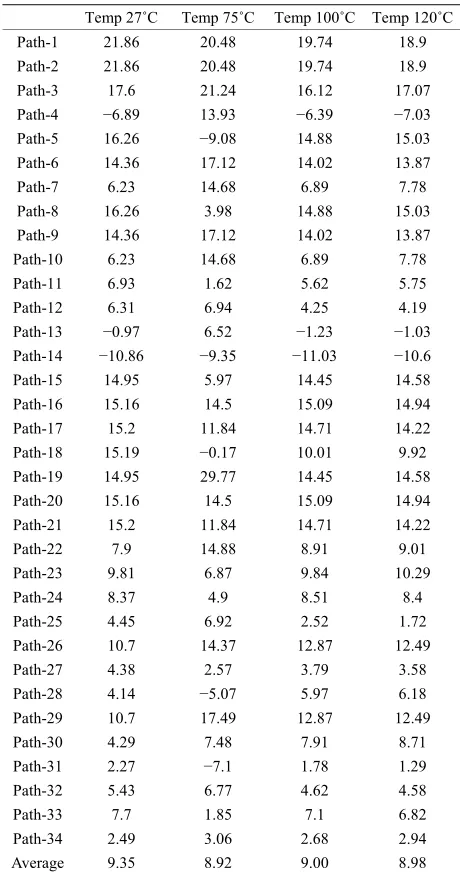
[image:3.595.306.539.101.262.2] [image:3.595.82.289.246.382.2]for 60.75% improvement as presented in Table 1. Table 2 shows the percentage reduction in delay sen- sitivity (τ= σ/μ) of 2-b WBTC at different operating tem- peratures. With an average 9% reduction in delay sensi- tivity, the CLO algorithm works efficiently at different temperatures. This reduction in delay sensitivity of criti- cal paths came at the cost of increase in delay sensitivity of non-critical paths (4, 5, 13, 14, 18, 28 and 31). Ranks from delays of these paths are shown in Table 3. In- crease in delay sensitivity of these paths is acceptable as majorityof paths except path-31 are not critical paths. Ef- ficiency of the CLO algorithm is further demonstrated through implementation on several circuits using IBM 130 nm CMOS process. The design profiles along with performance improvement are shown in Table 4, vali- dating that CLO algorithm works effectively for circuits
Table 1. 2-b WBTC delay c
Critical Worst-case delay (μ + σ) Delay uncer
path (psec) (psec)
0 1 355 158
1 1 244 112
2 1 209 91
3 3 185 84
4 25 171 77
5 19 170 76
6 25 166 72
7 21 166 65
8 25 161 67
9 8 157 57
10 25 157 5762
[image:3.595.307.537.298.734.2]Improvement (%) 55.77 60.75
Table 2. 2-b WBTC delay se sitivity improvement (%) at
emp 75˚C Temp 100˚C Temp 120˚C n
different temperatures.
Temp 27˚C T
Path-1 21.86 20.48 19.74 18.9
Path-2 21.86 20.48 19.74 18.9
Path-3 17.6 21.24 16.12 17.07
Path-4 −6.89 13.93 −6.39 −7.03 Path-5 16.26 −9.08 14.88 15.03
Path-6 14.36 17.12 14.02 13.87
Path-7 6.23 14.68 6.89 7.78
Path-8 16.26 3.98 14.88 15.03
Path-9 14.36 17.12 14.02 13.87
Path-10 6.23 14.68 6.89 7.78
Path-11 6.93 1.62 5.62 5.75
Path-12 6.31 6.94 4.25 4.19
Path-13 −0.97 6.52 −1.23 −1.03 Path-14 −10.86 −9.35 −11.03 −10.6
Path-15 14.95 5.97 14.45 14.58
Path-16 15.16 14.5 15.09 14.94
Path-17 15.2 11.84 14.71 14.22
Path-18 15.19 −0.17 10.01 9.92
Path-19 14.95 29.77 14.45 14.58
Path-20 15.16 14.5 15.09 14.94
Path-21 15.2 11.84 14.71 14.22
Path-22 7.9 14.88 8.91 9.01
Path-23 9.81 6.87 9.84 10.29
Path-24 8.37 4.9 8.51 8.4
Path-25 4.45 6.92 2.52 1.72
Path-26 10.7 14.37 12.87 12.49
Path-27 4.38 2.57 3.79 3.58
Path-28 4.14 −5.07 5.97 6.18
Path-29 10.7 17.49 12.87 12.49
Path-30 4.29 7.48 7.91 8.71
Path-31 2.27 −7.1 1.78 1.29
Path-32 5.43 6.77 4.62 4.58
Path-33 7.7 1.85 7.1 6.82
Path-34 2.49 3.06 2.68 2.94
e 3. 2-b C path s at different iterations and temperatures.
Temp Temp = 120˚C
Tabl WBT rank
= 27˚C Temp = 75˚C Temp = 100˚C
Iter-1 Iter-10 Iter-1 Iter-10 Iter-1 Iter-10 Iter-1 Iter-10
Path-4 23 8 24 9 25 10 25 10
Path-5 5 12 5 15 5 16 5 17
Path-13 25 11 25 10 24 9 24 9
Path-14 26 10 26 11 26 11 26 13
Path-18 9 21 9 22 9 4 9 4
Path-28 17 24 17 24 17 23 17 23
Path-31 13 2 13 2 13 2 14 2
[image:4.595.56.535.100.232.2] [image:4.595.59.540.259.449.2]Ratio did not decrease Ratio did not decrease and path became critical
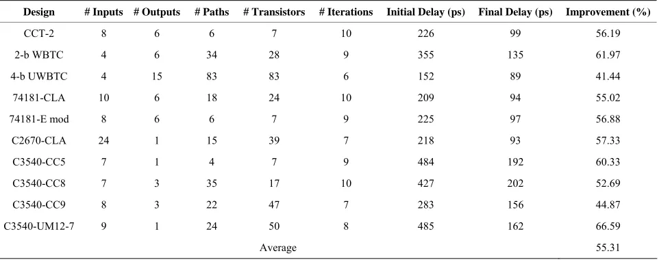
Table 4. Timing optimization esults from CLO algorithm.
Design # Inputs # Outputs ) Improvement (%)
r
# Paths # Transistors # Iterations Initial Delay (ps) Final Delay (ps
CCT-2 8 6 6 7 10 226 99 56.19
2-C
Average 55.31
b WBTC 4 6 34 28 9 355 135 61.97
4-b UWBTC 4 15 83 83 6 152 89 41.44
74181-CLA 10 6 18 24 10 209 94 55.02
74181-E mod 8 6 6 7 9 225 97 56.88
C2670-CLA 24 1 15 39 7 218 93 57.33
C3540-CC5 7 1 4 7 9 484 192 60.33
C3540-CC8 7 3 35 17 10 427 202 52.69
C3540-CC9 8 3 22 47 7 283 156 44.87
3540-UM12-7 9 1 24 50 8 485 162 66.59
4. Design Level Optimization through
Co sign and op-
common limitation in most de
dresses some of these challenge in timing optimization,
nd optimization tool along with design con- st
are replaced with black bo
Mixed-Static-Dynamic Circuits
nventionally, synthesis tools perform de
timization using static CMOS logic [13,14]. It is not un- common for the synthesis tools to not find an acceptable solution in terms of timing. This challenge can be an- swered through utilizing the advantage of fast timing in dynamic logic. Dynamic logic has smaller gate capaci- tances compared to their static CMOS counterparts, which accounts for a significant speedup [3,15]. With static and dynamic logic having their respective advantages of low power and low delay, an optimal balance can be obtained by partitioning the design to use both static and dynamic logic in an effective manner.
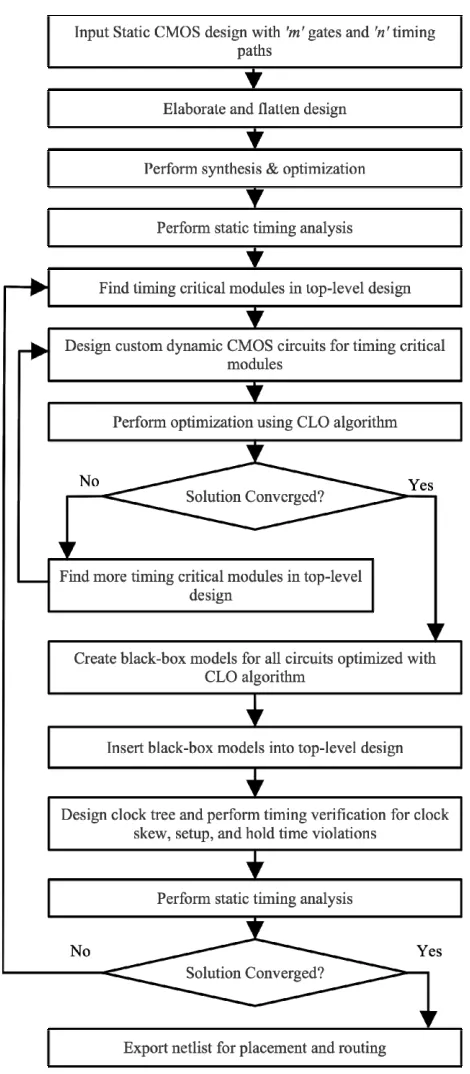
At the architecture level, a
sign optimization flows is the limited accountability for process variations. Typically after placement and route, if a design fails to meet the timing constraints, op- timization flow is re-iterated. Even after several itera- tions, design may still not meet the timing constraint, and miss the time-to-market window. The design level opti- mization (DLO) algorithm proposed in Figure 2 ad-
and also accounts for process variations. Utilizing the CLO algorithm proposed in previous section, the DLO algorithm partitions the design to effectively utilize both dynamic and static CMOS logic to meet the timing con- straints.
The high level description of a design is input to a synthesis a
raints and target library. After synthesis and optimiza- tion, Static Timing Analysis (STA) is performed to iden- tify the critical modules in the design. A strategy similar to the circuit level optimization algorithm is followed to find the critical modules in the design. These modules are identified based on the number (repeats) and length (weight) of critical paths in each. Once identified, custom dynamic CMOS circuits are designed at transistor level for greater flexibility, and timing optimization is per- formed using the circuit level optimization algorithm presented in the previous section.
Next, timing critical static CMOS modules from the commercial tool optimized design
Figure 2. Design level optimization algorithm.
circuit ock
skew, setup and hold time v lation) is performed. If the
emented ISCAS
5). Though STA, modules CC5 and
s, clock tree design and timing verification (cl io
timing constraints have been met, the design is exported for placement and routing. If not, the new timing critical modules are further identified and optimized using circuit level optimization algorithm presented in the previous section. This iterative process is a deterministic approach moving towards the optimum.
5. Implementation of DLO Algorithm
The design level optimization algorithm was impl on a number of combinational circuits, including
[image:5.595.308.540.380.531.2]benchmarks, and a high performance 64-b adder using IBM 130 nm CMOS process. Figure 3 shows the block diagram of the ISCAS benchmark c3540, an 8-b ALU with 1669 gates. After synthesis and optimization using the commercial tool, STA was performed. Delays of top 5 critical paths (highlighted) in c3540 were found to be 3.59 ns, 3.46 ns, 3.16 ns, 3.13 ns, and 2.97 ns respec- tively. Modules with highest delay in c3540 were found to be M5 with a delay of 1.63 ns, followed by M4 with a delay of 0.78 ns, and M12 with a delay of 0.63 ns (high- lighted in Figure 3). The modules chosen for timing op- timization from the STA are M5 and M12. Although M4 had the second highest delay, it was not chosen for opti- mization, as it does not repeat in as many critical paths as M5 and M12. This method of choosing only the critical modules during optimization is similar to circuit optimi- zation algorithm, and helps limit the increase in area and power consumption.
[image:5.595.313.534.560.719.2]Figure 4 shows the data flow schematic of M5-UM5_6 (critical module in M
Figure 3. ISCAS benchmark-C3540 [16].
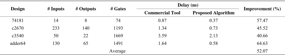
Table 5. Design level optimiz
Delay (ns) ation algorithm results.
Design # Inputs # Outputs # Gates
Commercial Tool Proposed Algorithm Improvement (%)
74181 14 8 74 0.87 0.37 57.47
c2670 233 140 1193 1.34 0.73 45.52
c3540 50 22 1669 3.59 2.13 40.66
adder64 130 65 1491 1.64 0.58 64.63
Average 52.07
CC9 are found to be critical modules (highlighted in Fig- ure 4), and are optimized using circuit level optimization algorithm. Accordingly, delays of these custom dynam CMOS circuits were reduced by
tively. Prior to implementing the circuit level optimiza-
tion a , CC5 ay i rst
stage of M5-UM5_6. This optimization reduced delay of CC5, de CC8 to he modu with highe ay in the tage of M M5_6. cceptable, as CC8 ot reside i he top 2 critical
C354 ot to limi overall ormance
A similar approach was followed in optimi 2- UM12_7 using the design level optimization algorithm,
e de- la
MOS logic ci with high number of timing paths. Second, we propose a
robust to process variation-aware load balance of multi- ple paths algorithm for timing optimization of dynamic CMOS logic. And last, we demonstrate the robustness of delay, delay uncertainty, and delay sensitiv her, this paper also presented a de- -
logi ented it on several
ISCA nchmark circui d a 64-b adder. Efficiency of th level optimi n algorithm flo rther valid hrough demon ng an average t-case
dela ment of 64 comparison w e-of-
the-art commercial optimization tools.
REFERENCES
ic
57% and 39% respec- algorithm in optimization of
lgorithm had the highest del n the fi
but ma be t le st del
first s 5-U This is a
does n n t 0% paths in
0 so as n t the perf .
zing M1
and its delay was reduced from 485 ps to 178 ps, a 63% improvement. One iteration of algorithm reduced delays of top five critical paths to 2.42 ns, 2.29 ns, 2.28 ns, 2.38 ns, 2.22 ns respectively. Through implementation of this optimization algorithm, the worst-case delay of c3540 was reduced from 3.59 ns to 2.13 ns, a 40% improvement over the results obtained from the commercially available state-of-the-art optimization tool. Similarly, the design level optimization algorithm was implemented on several other ISCAS benchmark circuits and a 64-b adder. Through implementation on c2670, the algorithm reduced th
y from 1.34 ns to 0.73 ns, a 45% improvement over the results obtained from acommercial tool. Also, the pro- posed algorithm reduced delay of 64-b adder from 1.64 ns to 0.58 ns. Timing optimization results obtained from the implementation of proposed design level optimiza- tion algorithm are shown in Table 5.
6. Conclusion
Effective performance optimization techniques are vital to the success of VLSI circuits as timing optimization and noise tolerance become ever-increasing problems with the relentless scaling of CMOS process technology. A desirable performance optimization technique should be able to improve the circuit robustness against all these challenges, be suitable for all logic functions, and have very low overhead in silicon area, delay, and power con- sumption. In this paper, such a performance optimization technique is proposed. First, we identify the complexity in timing optimization of dynamic C rcuits
ity. Furt ptimization al sign level o
namic CMOS
gorithm for c, and has implem
mixed-static-dy
S be ts an
e design zatio w is fu
ated t strati wors
y improve % in ith stat
[1] J. Tschanz, K. Bowman and V. De, “Variation-Tolerant Circuits: Circuit Solutions and Techniques,” Design AutomationConference, San Diego, 13-17 June 2005, pp. 762-763.
[2] P. S. Zuchowski, P. A. Habitz, J. D. Hayes and J. H. Oppold, “Process and Environmental Variation Impacts on ASIC Timing,” IEEE/ACMInternational Conference on Computer Aided Design, San Jose, 7-11 November 2004, pp. 336-342.
[3] M. Zhao and S. S. Sapatnekar, “Timing-Driven Partition- ing and Timing Optimization of Mixed Static-Domino Implementations,” IEEE Transactions on CAD of Inte- gratedCircuitsandSystems, Vol. 19, No. 11, 2000, pp. 1322-13360. doi:10.1109/43.892856
[4] J. P. Fishburn and A. E. Dunlop, “TILOS: A Posynomial Programming Approach to Transistor Sizing,” Interna- tionalConference on ComputerAidedDesign, Delft, 7-10 October 1985, pp. 326-328.
[5] V. Sundararajan, S. S. Sapatnekar and K. K. Parhi, “Fast and Exact Transistor Sizing Based on Iterative Relaxa- tion,” IEEETransactions on CAD, Vol. 21, No. 5, 2002, pp. 568-581.
[6] A. R. Conn, I. M. Elfadel, W. W. Molzen Jr., P. R. O’Brien, P. N. Strenski, C. Visweswariah and C. B. Whan, “Gradient-Based Optimization of Custom Circuits Using a Static-Timing Formulation,” DesignAutomation Conference, New Orleans, 21-25 June 1999, pp. 452-459. [7] K. A. Bowman, S. G. Duvall and J. D. Meindl, “Impact of
[8] P. S. Zuchowski, P. A. Habitz, J. D. Hayes and J. H. Oppold, “Process and Environmental Variation Impacts
Parameter Variations and Impact on
nsor for Nanometer on ASIC Timing,” IEEE/ACMInternationalConference on Computer Aided Design, San Jose, 7-11 November 2004, pp. 336-342.
[9] S. Borkar, T. Karnik, S. Narendra, J. Tschanz, A. Kesha- varzi and V. De, “
Circuits and Microarchitecture,” DesignAutomationCon- ference, Anaheim, 2-6 June 2003.
[10] C. H. Kim, K. Roy, S. Hsu, R. Krishnamurthy and S. Borkar, “A Process Variation Compensating Technique with an On-Die Leakage Current Se
Scale Dynamic Circuits,” IEEE Transactions on VLSI Systems, Vol. 14, No. 6, 2006, pp. 646-649.
doi:10.1109/TVLSI.2006.878226
[11] K. Yelamarthi and C.-I. H. Chen, “Process Variation-
SM.2008.2011665
Aware Timing Optimization for Dynamic and Mixed- Static-Dynamic CMOS Logic,” IEEE Transactions on
SemiconductorManufacturing, Vol. 22, No. 1, 2009, pp. 31-39. doi:10.1109/T
t Technology
l Confer-[12]V. Chandrasekhar, C.-I. H. Chen and K. Yelamarthi, “Low-
Cost Low-Power Self-Test Design and Verification for On-Chip ADC in System-On-a-Chip Applications,” IEEE Instrumentation and Measuremen
ence, Sorrento, 24-27 April 2006.
[13]Synopsys Design Compiler, http://www.synopsys.com [14]Cadence Encounter, http://www.cadence.com
[15]R. Puri, “Design Issues in Mixed Static-Dynamic Circuit Implementation,” Proceedings of Internationa
ence on Computer Design, San Jose, 5-7 October 1998, pp. 270-275.