Printed in U.s. America
Burroughs
MEDIUM
SYSTEMS
8 3700/8 4700
CENTRAL PROCESSOR
REFERENCE MANUAL
COPYRIGHT © 1966, 1968, 1969, 1972 AA828689 AA995115 AA 120798
Burroughs Corpora.tlon
Detroit. Michigan 48232
$2.00
INTRODUCTION . System Description
B 3700 . . . . . B 4700 . . . ' . .
TABLE OF CONTENTS
TITLE
Variable Field Length Floating Point (Optional) B 3700/B 4700 System Configurations
Data Representation . . . . Processor Instruction Format
Operation Code . . . Variant Digits
AF, BF Variants Indirect Field Length Literal
Addresses . . . . . Indexing . . . . . Indirect Addressing Extended Address Interrupts . . . .
Control State Interrupts Normal State Interrupts Logical Units . . .
Logic Section . . . . . Comparison Flip-flops Overflow Flip-flop Data Registers . Bussing . . . Arithmetic Section
Adder . . . .
Floating Point Arithmetic . . . . Floating Point Adapter (Optional) .
Fixed Length Arithmetic Unit . .
Accumulator, Exponent Register, Extension Register Adder . . . .
Scratchpad Memory Arithmetic Register Multiplier
Control Section . . . . In terru pts . . . . . Result Descriptors . . . Processor Result Descriptor
In valid IIO . . . . Invalid Instruction Memory Parity Error Address Error
Instruction Time-Out Timer . . . .
Operator Interrupt .
Normal/Control State Operation OP Register . . . . Logic Counter-Sequence Counter
iii PAGE 1 1 1 1 1 1 1 7 7 7 7 7 8 8 8 8 9 9 9 10 10 10 10 11 11 12 12 12 12 14 14 14 16 16 16 16 17 18 18 18 19 19 19 19 19 20 20 20 21 21
TABLE Of CONTENTS (Cont)
Addressing Section . . . Address Register . . . Base-Limit Registers Addressing Techniques Address Memory . ,
1/0 Address Memory
1/0 Address Register Memory Control Section
Translator . . . . . Error Correction
Operator Console and Display Operator Display
Console Controls Load Function .
Universal Load Normal Load . . Central System Power
+4.75, -2, DC Common
+
170 Volts . . . .+
12 Volts and+
10 Volts 30 Volts ACAir Sense . . . . Power OnlOff . . . .
+4 Volts, +22 Volts . . . . . . APPENDIX A B 3700/B 4700 Instruction Set
TITLE
LIST Of IllUS1RPi T~ONS
FIGURE 1 2 3 4 5 6 7 8 9 10 11 12 13 14 TABLE 1 TiTLE
Typical B 4700 Configurations Typical B 3700 Configurations Extended Address
Adder Functional Flow Chart Adder Examples
Fixed Length Arithmetic Unit Fixed Length Adder
Memory Allocation
RID Format
Processor Result Descriptor Operational Block Diagram
Interrupt and BRE Reserved Memory Error Correction
Processor Voltages
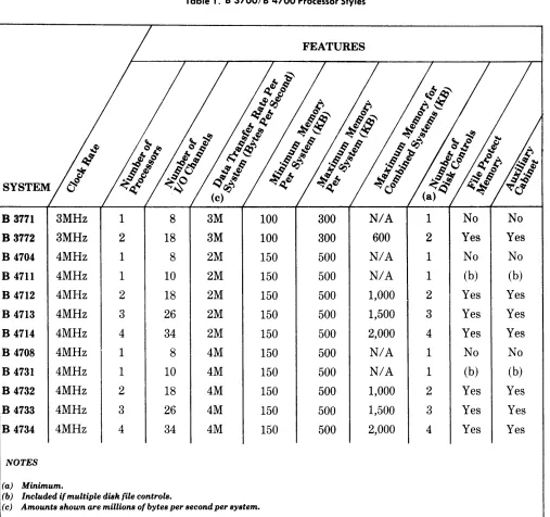
LIST Of l' ABLES TITLE B 3700lB 4700 Processor Styles
INTRODUCTION
The B 3700 system and the even more powerful B 4700 system constitute Burroughs response to the EDP equipment users' demand for more ef-ficient, faster, and more sophisticated data-processing systems. The B 3700 and B 4700 sys-tems are character-oriented toward business and data communications applications. They consist of highly efficient modular hardware/ program products, plus a wide range of excep-tional peripheral devices that fulfill the re-quirements involved in solving the data gathering and immediate response requIre-ments that confront data processing installa-tions today and in the near future.
It is the purpose of this manual to acquaint the reader with the Central Processor and asso-ciated components offered by Burroughs Cor-poration which are applicable to the B 3700 and B 4700 systems.
SYSTEM DESCRIPTION
B 3700
The B 3700 is characterized by a 3 MHz clock speed and a memory cycle time of 667 nanoseconds. Memory sizes range from 100,000 to 300,000 bytes of solid state (IC) memory. A unique method of overlapping memory cycles has been implemented in the B 3700, to enhance the processor's response characteristics during high I/O activity periods. Due to this feature, an I/O bandpass of 3 million bytes per second is possible.
The B 3700 can accommodate up to 20 concur-rent I/O channels, 10 for high speed peripheral subsystems and 10 for low speed peripheral de-vices. The I/O subsystem can be expanded to accommodate integrated data communication controls which will accommodate up to 36 lines.
B 4700
The B 4700 system has a higher clock rate (4 MHz) than does the B 3700. The B 4700 has the
-1-B 3700/-1-B 4700
CENTRAL PROCESSOR
capability to handle 20 standard I/O channels,
or up to 56 channels for data communication applications. The memory subsystem may con-tain up to one million directly addressable dig-its of high-speed core memory having a cycle time of 500 nanoseconds.
Both systems can utilize all medium systems peripheral devices as well as the full mix of me-dium systems controls, exchanges and adapters.
Power for the system, excluding peripheral
de-vic~s, is deri.ved from one central power supply,
whICh contaIns all the required regulator and sensing circuitry. These supplies are internally compensated so as to reduce to a minimum any power fluctuation to the system. Several detectors are utilized to sense fault conditions such as low input voltage, dropped cycles, or in-put voltage that is too high. In addition, tem-perature sensors are employed to warn users of excessive room temperature.
Variable Field Length Floating Point (Optional)
This adapter is available for those users who require the Floating Point commands, OP 80 through 83. Installation of this adapter enables the user to perform real-arithmetic operation with
~p
to 100 digits of accuracy. Basically,th~
functIOn of this adapter is to handle the align-ment and normalization of operands as general-ly required in real-arithmetic operations.B 3700/B 4700 SYSTEM CONFIGURATIONS
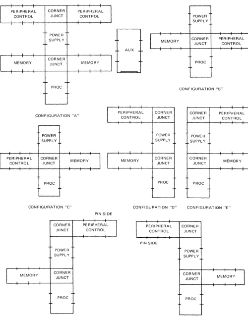
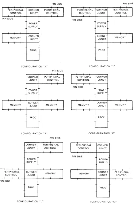
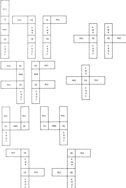
The configurations for the B 3700 and B 4700 systems are described in table 1, which lists various cabinets and operating characteristics. Figure 1 shows various B 4700 configurations and figure 2 shows the typical B 3700
equip~
ment configurations.DATA REPRESENTATION
The basic unit of data used in the B 3700 and B 4700 processors is the bit, which represents
the presence or absence of a specific piece of in-formation. By assigning particular values to specific bits, these bits can be combined to form larger, more efficient units of information. Be-cause of the overall system orientation toward COBOL and the business applications by the majority of users, analysis indicated that four bits would be the optimum size of this unit of information, designated as the digit. By as-signing binary weights of 1, 2, 4, and 8 to each of the bits, the combined value can represent any number from 0 through 15. The digits
shown below illustrate how various bit combi-nations are used to represent numerical values:
8 Bit 1 0 1 1
4 Bit 0 1 1 0
2 Bit 0 0 0 1
1 Bit 1 1 0 1
(A) (B) (C) (D).
Table 1. 8 3700/8 4700 Processor Styles
FEATURES
B 3771 3MHz 1 8 100 300
N/A
1 No NoB3772 3MHz 2 18 3M 100 300 600 2 Yes Yes
B 4704 4MHz 1 8 2M 150 500
N/A
1 No NoB 4711 4MHz 1 10 2M 150 500
N/A
1 (b) (b)B 4712 4MHz 2 18 2M 150 500 1,000 2 Yes Yes
B 4713 4MHz 3 26 2M 150 500 1,500 3 Yes Yes
B 4714 4MHz 4 34 2M 150 500 2,000 4 Yes Yes
B 4708 4MHz 1 8 4M 150 500
N/A
1 No NoB 4731 4MHz 1 10 4M 150 500
N/A
1 (b) (b)B 4732 4MHz 2 18 4M 150 500 1,000 2 Yes Yes
B 4733 4MHz 3 26 4M 150 500 1,500 3 Yes Yes
B 4734 4MHz 4 34 4M 150 500 2,000 4 Yes Yes
NOTES
(a) Minimum.
(b) Included if multiple disk file controls.
[image:6.612.66.573.259.735.2]I r I
I I
PERIPHERAL CORNER PERIPHERAL
-CONTROL JUNCT CONTROL POWER
I 1 I I I SUPPLY
I I I
-~ POWER -I- ~
.
.
SUPPLY
-I- -~
-r- CORNER PERIPHERAL
MEMORY
JUNCT CONTROL
.
AUX -~ T
I I I I
I
CORNER .~
MEMORY JUNCT MEMORY PROC
-I-I I I r
I I I I
-~
-PROC CONFIGURATION "8"
-~ -~
I I
CONFIGURATION "A" PERIPHERAL CONTROL CORNER JUNCT CORNER PERIPHERAL JUNCT CONTROL
.
POWER POWER POWER
SUPPLY SUPPLY _~ SUPPL Y
I ,
MEMORY CORNER JUNCT PERIPHERAL CORNER
MEMORY CONTROL .IUNCT
CORNER
MEMORY JUNCT
I I 1 1 ,
to -~
PROC PROC PROC
-~
CONFIGURATION "C" CONF IGURATION "0" CONFIGURATION "E" PIN SIDE
CORNER PERIPHERAL PERIPHERAL CORNER
JUNCT CONTROL CONTROL JUNCT
I ,
PIN SIDE
-
POWER r- POWER .SUPPLY
-
SUPPLY.
--'MEMORY CORNER JUNCT
CORNER
MEMORY JUNCT
I I I
-r- + -~ ~
PROC PROC
I- -~ to -~
CONFIGURATION "F" CONFIGURATION "G"
Figure 1. Typical B 4700 Configurations (Sheet 1 of 2)
[image:7.624.46.547.61.701.2]PIN SIDE PIN SIDE I PERIPHERAL CORNER PERIPHERAL PERIPHERAL CORNER PERIPHERAL
CONTROL JUNCT CONTROL CONTROL JUNCT CONTROL
I I
PIN SIDE
PIN SIDE
r
POWER POWER
SUPPLY . SUPPL Y
I
, , I
MEMORY CORNER JUNCT
CORNER
JUNCT MEMORY
I j I
~
PROC PROC
I-
I-CONFIGURATION "H" CONFIGURATION "I" PIN SIDE
CORNER PERIPHERAL PERIPHERAL CORNER
JUNCT CONTROL CONTROL JUNCT
I I
,
PIN SIDE
--POWER POWER
SUPPLY
~ -I- l- SUPPLY
I-I I I I I
CORNER CORNER
MEMORY JUNCT MEMORY MEMORY JUNCT MEMORY
I I I I 1
I
- l-
I-PROC PROC
+
I-CONFIGURATION "J" CONFIGURATION "K" PIN SIDE
CORNER PERIPHERAL PERIPHERAL CORNER
JUNCT CONTROL CONTROL JUNCT
r- PIN SIDE
POWER POWER
SUPPLY SUPPLY
-PERIPHERAL CORNER
CONTROL JUNCT MEMORY MEMORY
CORNER PERIPHERAL JUNCT CONTROL I
PIN SIDE
-PROC PROC
-CONFIGURATION "L" CONFIGURATION "M"
[image:8.615.95.530.68.728.2]pee
es pee es es pee
p p p P
PWR W W W W
R R R R
es es cs pee es es pee
P p P P
R R R R R
a a a a a
e e e e e
I
pee es es pee1
PW
PWR PWR R
[
pee es es peeI
pee es pee
P
p P R
R R a
a a e
e e
L - - - "
-. - - - - ..---- .---- .
-pee pee pee pee
es PWR es es PWR es
P P
R R
a a
e e
L - - - L . . .
-l
pee es cs pee1
P P
w W
R R
es pee
I
I
pee csP P
R R
a a
e e
L . . . . - - - '
-Figure 2. Typical B 3700 Configurations
[image:9.623.75.508.61.706.2]In these examples, the presence of a bit is indi-cated by a 1 in the particular cell, and the ab-sence of the bit is represented by a O. In A above, both the 8-bit and the I-bit are present, so the digit value is 9. The next digit, B, has the 4 and 1 bit present, representing a decimal 5. The last two columns, C and D, represent decimals 12 and 11, respectively, and as such cannot be represented as a normal decimal dig-it.
These special cases of digits having numeric values greater than 9 10 are called undigits and
are represented either by alpha characters or by a slash through the units portion of the decimal value as shown below:
DIGITIO
10
11 12
13
14
15
REPRESENTED AS:
IN PRINT
A B
c
D E
F
ON CONSOLE DISPLAY
The digit is the basic unit addressable by the processor, and is the smallest unit of data avail-able to the user.
As previously stated, the digit can only repre-sent values of from 0 to 15, or 16 discrete states. Since this is not enough to represent all the possibilities of numeric digits, alphabetic characters and special symbols used in the data processing field, two digits are combined to form the unit of data called the byte, which has the ability to represent a total of 16 x 16, or 256 discrete values.
The byte, shown below, can be used to repre-sent any alphanumeric or special character in either EBCDIC or ASCII.
8 8
4 4
2 2
1 1
A byte is often referred to as a character; how-ever, this is not entirely accurate. The byte is the measure of a quantity of data, which may or may not represent a character; however, a character is a specific array of bits that conveys some usable intelligence.
A word, as used in B 3700 and B 4700 systems, consists of four contiguous digits, beginning and ending at specific locations in memory. As shown below, the four digits are identified as A, B, C, and D, with each bit of each digit being identified according to its binary value. Words must begin at MOD 4 addresses; that is, ad-dresses that are evenly divisible by four.
8
Bits 4
2
1
A A8
A4
A2
Al
DIGITS
B B8
B4
B2
Bl
C D
C8 D8
C4 D4
C2 D2
Cl Dl
Because many instructions use word-oriented data fields, the ability to address to a word lev-el, and subsequently manipulate these large data blocks, rather than repetitively handling smaller units, affords a higher efficiency level and a significant increase in system throughput.
of signed numeric, a sign digit is placed before the data field. If the instruction specified alpha information, the data field is treated as groups of 8-bit bytes.
PROCESSOR INSTRUCTION FORMAT
Processor instructions may vary in length from 4 to 24 digits and have from none to three ad-dresses as shown below:
a. OP VV
b. OP AAAA
c. OP AAAAAA
d. OP AFBF AAAAAA BBBBBB
e. OP AFBF AAAAAA BBBBBB CCCCCC
In the above example, OP indicates the operation code, VV indicates variant digits, AF and BF represent the A and B field variant dig-its, and A, B, and C represent the addresses of the respective data fields. In all cases, each let-ter represents one digit of instruction informa-tion.
Operation Code
The first two digits of any instruction always represent the operation (OP) code. This OP code is indicative of the length of the instruction and, more importantly, informs the processor of the type of action to take on the specified data.
Variant Digits
These digits, when used in instructions such as shown in the previous example, give the proces-sor more detailed information on how to handle the specified data.
AF, SF Variants
Generally, these digits specify the length of the "A" data field and the "B" data field, respec-tively. Since both AF and BF are 2-digit fields, each may specify a length of 00 to 99, with 00 representing a length of 100. In some instruc-tions, AF and BF may be combined to represent lengths of from 0000 to 9999, with 0000 repre-senting a value of 10,000. The significance of
-7-the value of -7-the AF and BF variants is deter-mined by the contents of the "A" field and "B" field, respectively.
Indirect Field Length
Another function available within the variant fields, when their use within an instruction specifies field length, is that of indirect field length. When the two high-order bits (8 and 4) of the most significant digit of AF or BF are ON, they indicate an indirect field length. The two low-order bits (2 and 1) plus the entire least significant digit indicate the tens and units dig-its of an address where the field may be found. This address must be an even number. For ex-ample:
Indirect field 8
length is 4
indicated.
Tens position of 2
the address 1
where the field can be found.
x
X X NOTE X X 8 4 2 1Units position of the address
where the
field length can be found.
X indicates the bit is ON. Blank in-dicates OFF.
In this example, the variant reflects that an in-direct address contains the field length of the instruction being executed and that the length of the field is to be found at base relative ad-dress 00016.
While it is logically possible to use indirect field length to any depth, it is obvious that the num-ber of addresses generated by the technique is limited. The two low-order bits of the high-or-der digit may represent values of 0, 1, 2, or 3. Since the address must be even, the range may be from 00000 to 00038, base relative. This tech-nique can be very useful in cases where many instructions in a program refer to the same field, and that field is variable in length. The field length may be modified in only one loca-tion. All instructions referring to that field will be so modified without the necessity of any oth-er code change.
Literal
Another use of the AF variant is to indicate that the A syllable of the B 3700 and B 4700 Systems command does not contain an address, but instead contains literal data to be used di-rectly by the command. This option is indicated by the 8-bit and the 2-bit, in the most significant digit of the AF field, being ON, with the 4-bit being OFF. A literal, as with any data, may be represented as 4-bit digits, either signed or unsigned, or as 8-bit characters. The l:.bit of the most significant digit of AF and the 8-bit of the least significant digit are used to indicate the internal representation to be used for the literal and are called controller bits which rep-resent the following 27'bit values:
a. 0 - unsigned numeric (4-bit mode).
b. 1 - signed numeric (4-bit mode).
c. 2 - alphanumeric (8-bit mode).
d. 3 - unused.
The remaining three bits of the low-order digit of AF specify the length of the literal. Since the A syllable is six digits in length, the following lengths are maxim urn:
a. Unsigned numeric - six 4-bit digits.
b. Signed numeric - five 4-bit digits plus a sign 4-bit digit.
c. Alphanumeric - three 8-bit (byte) charac-ters.
For example:
8-bit and 2-bit, being ON, indicate that a literal is present in the A address portion of the instruction.
8
4}
Indicate that the length 2 - of the literal is 6.1
In the example, bl and b2 both being OFF indi-cate an unsigned numeric representation. The A syllable contains a literal of six unsigned nu-meric digits.
All field lengths specified for signed numeric fields reflect the length, excluding the sign. In floating-point instructions, field length reflects the length of the mantissa only.
Addresses
Typically, data field addresses have six digits, the most significant of which is used to flag such functions as indexing, indirect addressing, or extended addressing. The remaining five (or in the case of extended addressing, six) digits constitute the base relative address of the data field.
INDEXING
The eight-and four-bits of the most-significant digit of the address are used to specify indexing with anyone of the three programmable index registers available to each program. The condi-tion of these bits indicates which index register is to be used, as shown below:
8 4
Bit Bit
0 0
0 1
1 0
1 1
No indexing
Index Register 1 (I x 1)
Index Register 2 (I x 2) Index Register 3 (I x 3)
If indexing is specified, the value of the index register is algebraically added to the address field prior to storing the address in address memory.
INDIRECT ADDRESSING
EXTENDED ADDRESS
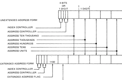
If the second digit of an address is a binary 12 (undigit 2), the following six digits constitute an address having the capability to address full memory (1,000,000 digits). Figure 3 illustrates the extended address and its flag compared to a normal unextended address.
4 BITS OR
the operating system examines the cause of the interrupt and determines the action to be taken.
Interrupts may occur while the processor is in either normal or control state. Their handling is somewhat different under the different con-ditions.
1 DIGIT
I I
: 1 DIGIT:
UNEXTENDED ADDRESS FORM INDEX CONTROLLER
ADDRESS CONTROLLER - - - ' ADDRESS TEN THOUSAND
ADDRESS THOUSANDS ADDRESS HUNDREDS ADDRESS TENS
ADDRESS UNITS ---. ---+---+---+----~--__4
EXTENDED ADDRESS FORM INDEX CONTROLLER ADDRESS CONTROLLER EXTENDED ADDRESS FLAG ADDRESS HUNDRED THOUSANDS
Figure 3. Extended Address
All capabilities assigned to normal addresses, incl uding indexing, indirect addressing, and literal capability, apply to extended addresses.
INTERRUPTS
In order to make most efficient use of available system resources, an interrupt scheme had to be designed into the B 3700/B 4700 systems. As a result, the processor has been freed from time-consuming monitoring tasks and allowed to function with as little interference as possi-ble. When some event does occur that requires processor action, the Interrupt flag is set, and
-9-Control State Interrupts
When the processor is operating in control state, there may be interrupt conditions generated, but no automatic interrupt handling takes place at the completion of an instruction. Rather, at the time that the MCP attempts to return to normal state, automatic branching to control location 000094 will occur so that these inter-rupts will be handled by the MCP.
If the processor is operating in the zero-base state, the following processor conditions will caU8e the processor to branch to control location 000094:
a. Memory parity error interrupt.
[image:13.623.84.496.207.478.2]b. Address error interrupt. c. Instruction time out interrupt. d. All non-assigned operator codes.
e. Operator codes requiring options which are not present.
f. Invalid halts.
Since the processor is in the zero-base state, any of the above interrupts indicates that a hardware or an operating system error exists. A privileged instruction interrupt cannot occur because all of the instructions are executable in the zero-base state. The clock interrupt condi-tion occurs in the same manner as in normal state, but no automatic branching occurs in control state.
Normal State Interrupts
When certain operational conditions occur within the processor while executing instruc-tions in the normal state, the following logic oc-curs:
a. If either an operator interrupt, a timer in-terrupt, or an I/O interrupt occurs, the inter-rupt will generate a result descriptor and store the descriptor in the reserved memory location.
b. The interrupt will set the interrupt flag and store the program return point and logical register settings.
c. An automatic branch is taken to the ad-dress specified by the contents of reserved memory location 000094. The processor oper-ational mode is changed from normal state to control state, zero base.
The branch to the control state is a branch to the operating system - the Master Control Program. It is the function of the operating sys-tem to determine the type of interrupt and the course of action that is to be followed. The in-terrupt system, as explained, is automatic and is an integral part of the processor hardware systeln.
LOGICAL UNITS
Functionally, the processor may be divided into four broad areas: a logical or data section, an arithmetic section, a control section, and an ad-dressing section. Each of these areas is subdivided into smaller, more specialized func-tional modules, and each is intimately associ-ated with the other sections.
Logic Section
The first of these' major areas, the logic section, consists of the data comparison circuitry, the overflow flag, several data registers and the busses required to transfer data throughout the system.
COMP ARISON FLIP-FLOPS
Two hardware flip-flops make up the comparison logical unit. These two flip-flops have the following four combinations (0 = OFF, 1
=
ON):a. 00 - cleared.
b. 01 - greater or high comparIson result. c. 10 - less or low comparison result. d. 11 - zero or equal comparison result. These four states represent the result of ex-ecuting an instruction that affects these logical units. The cleared state indicates that there is no comparison result existing. The instructions that set a result into the comparison flip-flops, which are displayed on the appropriate console indicators, are:
a. All arithmetic instructions. b. All floating point instructions. c. Compare instructions.
d. Move Numeric instruction. e. Move Alphanumeric instruction. f. The bit test instructions.
h. The scan instructions.
i. The Edit instruction.
j. The Scan Result Descriptor instruction.
k. Search instructions.
Any branching that is done on the basis of t~e
comparison flip-flops does not change theIr status. Only another instruction that affects them can change their status. When entering control state by means of the Branch Commu-nicate instruction or the automatic interrupt system, the status of the comparison flip-flops is stored. The 2-bit and l-bit of the same char-acter that stores the overflow flip-flop status will contain the status of the comparison flip-flops. The flip-flops are then cleared befo~e
branching to control state. When return IS made to the normal state, the Branch Reinstate. instruction will restore the comparison flip-flops from the character i,n re-served memory. Similarly, when entenng a subroutine the Enter instruction stores the
compariso~
flip-flops in the 2-bit and l-bit ofthe specified character in the memory stack. This same character contains the overflow flip-flops status. When leaving the su.brouti.ne with the Exit instruction, the companson fhp-flops are restored from this character in the stack.
OVERFLOW FLIP-FLOP
The overflow flip-flop is a hardware :ogical unit that indicates the data field of a move or arithmetic instruction is exceeded. If an over-flow condition is detected, the command is ex-ecuted but the data is not affected. The over-flow flip-flop is not cleared at the beginning of an arithmetic operation, therefore, it indi-cates overflow that has occurred any time before or during a series of arithmetic tions or other interjected nonarithmetic opera-tions. Instructions that can create an overflow condition are:
a. Arithmetic instructions except Multiply.
b. Floating point arithmetic instructions.
c. Move Numeric.
-11-d. Move Alphanumeric.
e. Fixed Length. Arithmetic Instructions.
Overflow cannot occur during a Multiply in-struction since the receiving field is always large enough to contain the product. In all cases except the floating point lnstructions, overflow results when the receiving field can-not contain the sending field. With floating point instructions, the overflow can also be. caused by an out-of-range exponent. The over-flow flip-flop is turned OFF by the Branch On Overflow instruction. Once cleared, it can be turned ON if the conditions arise while execu-ting those instructions that may turn it ON. There are two ways by which the present set-ting of the overflow flip-flop may be stored in the 4-bit of reserved location 000076, after which the flip-flop is cleared. These are:
a. Branch Communicate.
b. Automatic interrupt feature.
The overflow flip-flop is restored from the re-served memory location by the Branch Reinstate instruction. In addition, the object program may branch to some subroutine and the overflow flip-flop setting must be retained and restored at the conclusion of the subrou-tine execution, prior to continuing in the ob-ject program. The Enter instruction will store the flip-flop setting into the four bits of the reserved character location in the memory stack and then clear the overflow flip-flop. The Exit instruction will restore the overflow flip-flop setting from this reserved location.
DATA REGISTERS
Both the B 3700 and the B 4700 make exten-sive use of internal data registers so as to al-low a constant fal-low of fully buffered data, thus eliminating adverse effects to system per-formance. Various instructions use these buf-fer registers to hold arithmetic operands, data read from or to be written into memory, or data upon which comparisons are to be made. When used in arithmetic operations, some of these data buffers have the ability to automat-ically form the complement of the number they contain, thus reducing the arithmetic cy-cle times.
BUSSING
In order to rapidly and efficiently move data from point to point within the processor, all registers and buffers must have some sort of interconnection scheme. By using a polynodal bussing network and the appropriate control signals, it is possible to transfer data into and out of registers without error or loss, all with-in a few billionths of a second. This concept is used extensively throughout the B3700 and B 4700 processors. The speed of data transfers using this bussing technique is such that in many instances the only delay is that imposed by the propagation time of an electrical impulse through the system interconnections. Dependent upon the OP code, the processor generates the proper control signals to switch data from a selected source onto the busses, and then into the destination register.
Arithmetic Section
This area of the processor consists of the variable field length arithmetic unit or adder, the fixed field length arithmetic unit, and the floating point adapter. The Floating Point adapter is optional with either system. Variable field length arithmetic capability is standard on both processors.
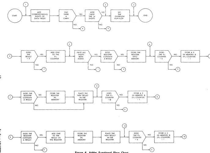
ADDER
The processor uses an adder that accumulates two fields from the most significant to the least significant digit positions. Reverse addition, as incorporated in B 3700 and B 4700 systems, has the advantage of detecting an overflow condi-tion prior to altering the receiving field for the result. The principle used in this type of adder is illustrated by the flow chart in figure 4 and the five examples in figure 5. If the data fields are signed, sign manipulation takes place prior to the addition since they are the most significant digits.
In figure 5, there is no manipulation of signs shown. The addition of two data fields is only shown to present the technique of a left-to-right adder.
In example 1, as each set of digits is added, no carry is generated and no nines are produced. As each new result is generated by the adder,
the previous result is stored in the result field. In example 2, an overflow condition is immediately detected because of a carryon the first digit addition. In example 3, the first five nines are not stored until the result equal to eight is generated. The eight is retained until the carry is generated when adding the last digits, at which time the eight is made into a nine and stored. The following nines are then stored as zeros in the receiving field, and then the final digit (8) is stored. Nothing is stored in example 4 until the final digits are added. The receiving field in example 5 remains unchanged even though an overflow condition is not detected un til the final digits are added. This is due to the result being contained in the nine's counter of the adder.
FLOATING POINT ARITHMETIC
In order to represent very large or very small numbers using decimal notation, a great many digits must be used. To simplify calculations, "powers of ten," or standard notation, has long been used. For example, the decimal value of 1,000,000 could be shown in standard notation as 1 x 10⁹
• Numbers in this format can be ma-nipulated using normal algebraic procedures far more simply than if they were shown in decimal format.
Floating point arithmetic slightly modifies this standard notation to a format more usable in computers. In floating point format, the num-ber 1 000 000 becomes +09+000001 when the , ,
field length specifies six digits. The general for-mat for any floating point number is shown be-low,
EX
~
II
MANTISSAI
Where SX is the one-digit sign of the exponent, EX is the two-digit exponent, and SM is the one-digit mantissa sign. The mantissa may be from 1 to 100 digits in length, as specified by the appropriate field variant (AF or BF). Both the exponent and the mantissa are integers.
"'T1 ~ "'T1 o
3
ADD CORRESPOND I NG t---'---o-t DIGITS OFDOES THE RESULT
= 9
DOES THE REGISTER CONTAIN
A RESULT
DOES THE REGISTER CONTAIN A RESULT
DATA FIELDS
YES
ADD ONE TO THE
9'5
COUNTER
STORE THE REGISTER
IN MEMORY
ADD ONE TO THE RESULT IN THE REGISTER
WAS THERE
A CARRY
YES
HAVE ALL DIGITS
BEEN ADDED
PLACE THE NEW RESULT
IN THE REGISTER
STORE THE REGISTER
IN MEMORY
WERE THESE THE 1st DIGITS
YES
YES SET THE OVERFLOW FLIP-FLOP DOES REGISTER CONTAIN
A RESULT
DOES THE 9'5
COUNTER =0
PLACE THE NEW RESULT
IN THE REGISTER
YES
NO
10
Figure 4. Adder Functional Flow Chart
STORE THE REGI STER
INTO MEMORY
STORE A 9
IN MEMORY &
(9'5 COUNTER)
- 1
DOES THE 9'5
COUNTER = 0
DOES THE 9'5
COUNTER
= 0
STORE A 0
IN MEMORY &
(9'5 COUNTER) - 1
STORE A 9 IN MEMORY &
[image:17.799.45.732.43.545.2]EXAMPLE 1:
12343 12343 RESULT 24686
EXAMPLE 2:
12345 92345 RESULT 1: 0 + CARRY
FINAL RESULT: OVERFLOW FLIP-FLOP SET
EXAMPLE 3:
876543229 123455779
RE SU L T 1: 999998998 + CARRY FINAL RESULT: 999999008
EXAMPLE 4:
0876543 0123457
RESULT 1: 0999990 + CARRY FINAL RESULT: 1000000
EXAMPLE 5:
876543 123457
RESULT 1: 999990 + CARRY
FINAL RESULT: OVERFLOW FLIP-FLOP SET
Figure 5. Adder Examples
since this is the smallest value the notation can represen t. Leading zeros in non -zero mantissas are acceptable in addition or subtraction; how-ever, in multiplication or division they will cause the entire mantissa to be treated as a zero and yield erroneous results.
FLOATING POINT ADAPTER (OPTIONAL)
The purpose of the floating point adapter is to manipulate the exponents and mantissas so that the numbers are aligned properly. This means that the exponent must either be decremented and the mantissa multiplied by 10 for each decrement of the exponent, or the ex-ponent incremented and the mantissa divided by 10 for each time the exponent is incre-mented. The net effect of these rnanipulations does not change the value of the number, but it does position the digits properly so that they may be added or subtracted.
In addition to the alignment function for addi-tion and subtracaddi-tion, this adapter also performs a normalizing function for multiplication and division.
Normalization (elimination of leading zeros) is accomplished by examining the leading digit of the product or quotient and, if zero, multiplying the result field by 10 with a corresponding dec-rement of the exponent.
FIXED LENGTH ARITHMETIC UNIT
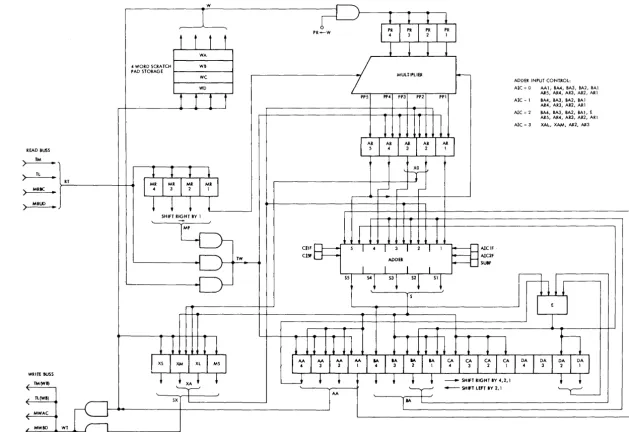
This portion of the processor makes use of sev-eral innovative techniques in arithmetic data manipulation; these include word-wide trans-fers into and out of the various arithmetic reg-isters, multiple shift capabilities, automatic overflow compensation, and a full word multi-ply capability. This unit consists of several ma-jor elements and their associated controls and interconnections as described below and illus-trated in figure 6.
[image:18.612.72.313.91.632.2]I
....
'f
. " ~ . " o
3
) ) ) )
READ BUSS TM TL MRIC MRW
.
.
.
.
WRITE BUSS " TM~B)
"'
" Tl(WI)
"'
" MWAC
"'
~ MWBD
"'
RT
WT
W
I
~
~l
PR-W PR PR PR
I I I I
4 3 IWA 4 WORD SCRATCH Wi PAD STORAGE
MULTIPLIER I -WC
/
ADDER INPUT CONTROL: WD Ale = 0 AAI, BM, BA3, BA2, BAIAR5, AR4, AR3, AR2, ARI
! i
PP5 PP4 PP3 PP2 PPIAIC = I BA4, BA3, BA2, BA I AR4, AR3, AR2, ARI AlC = 2 BA4, BA3, BA2, BAI, E
1
1
AR5, AR4, AR3, AR2, AR I AlC = 3 XAL, XAM, AR2, AR3
•
AR AR AR
~~Rl~J
5 4 3
I
~~IT-~ MI
I
~R ~RI
~RI
- r - - r-! -! -!
l
SHIFT RIGHT BY I
T 1
ta-
l
1
CI1F
B==:
5 I 4 I 3 I 2 I I:=§MO'
ClSf AlC2F
TW ADDER
SUIF
I I I I
iJh
II
D-
S5 54 53 S2SI
!.
SI
EI
-.
1
I T 1
h
I
I 1
1 11 11
1
1
1
I
xsI
XM
I
XLI
MSI
l~l~l'tI'l'I-:1
I ...
~I~I~I~I~I~I~I~I~I~I
3
•
l;J
•
~• •
~ ~~
- SHIFT RIGHT IY 4,2, I~
JAA
- SHFT LEfT IY 2, I
SX I IA L
[image:19.798.90.719.61.493.2]ADDER. The adder used in the fixed length arithmetic unit provides the capability to add or subtract two groups of five digits each and provides a decimally corrected result. As shown in figure 7, the adder consists of four major areas: input gating, hexadecimal adder, carry logic, and decimal correction logic. The input gating logic selects the two registers which are to be added or subtracted. In most cases, the inputs will be the B word of the accu-mulator and the AR register. Other com-binations may call for the inclusion of the E register or perhaps the addition of the operand exponents.
The hexadecimal adder and its associated carry logic work together to provide parallel five-digit addition. Since these are decimally oriented systems, hexadecimal results must be con-verted to decimal formats. The carry logic partially provides for this conversion by han-dling any carry from sums greater than nine and propagating carries through intermediate carry generating sums.
Decimal correction logic is used when the sum of an addition is greater than nine. As shown below, then 6 is added to the hexadecimal sum, the final sum is the correct decimal value:
9
+8
I I
+ - - - hexadecimal sum+6
17
+ - - - corrected decimal sumThe decimal correction logic is, in effect, a sec-ond stage of the adder which forces the addition of a 6 to the hexadecimal result.
SCRATCHP AD MEMORY. Four words of high-speed scratchpad memory are provided for temporary operand storage during the execution of the instruction. Data may be shifted from the accumulator into any of the four words, or from the scratch pad to one of the arithmetic registers.
ARITHMETIC REGISTER. This register, des-ignated AR in figure 6, is most commonly used as one of the inputs to the five-digit adder. It is a full five-digit register and may receive data from the multiplier, the MR register, or directly from memory. This register has no shift capability.
MULTIPLIER. The multiplier makes use of two registers, the four-digit PR and the shiftable four-digit MR, along with read-only memory look-up tables and adder circuitry. The basic algorithm for the multiply operation is as follows:
1. Multiply all four digits of PR by the least-significant digit of MR. This is done by us-ing the digit values in PR and MR as ad-dresses in the ROM look-up tables.
2. Add the 4 two-digit products to form 1 five-digit partial product.
3. Shift MR right one digit.
4. Multiply, add, and shift as in 1, 2, and 3 until all digits have been multiplied.
INPUT HEXADECIMAL DECIMAL
SUM
--+ GATING
-ADDER
-
CORRECTION-OPERANDS
•
•
CARRY LOGIC
[image:20.617.87.531.507.712.2]5. After each step 2, the partial products must be added, thus building the final prod-uct.
Control Section
This section of the processor is used to control and monitor internal system operation and to generate information for use by the operating system regarding processor status. Included in these control elements are the Normal flip-flop, the Interrupt flip-flop, result descriptors, Mode flip-flop, and the Timer.
The operation of the B 3700/B 4700 systems is controlled by the MCP. This control program, which resides in memory starting at address zero, performs all of its functions with the base register equal to zero and the processor in con-trol state. With the base r~gister equal to zero the following operational conditions exist:
a. Privileged instructions are valid.
b. Such processor errors as a memory parity error, memory address error, invalid instruc-tion, and instruction time-out will cause the operation of the system to be stopped. When in control state, the operation of the processor is not sensitive to the setting of the Interrupt flip-flop. An interrupt will be ignored until it is programmatically sensed by the con-trol program.
All object programs are loaded into memory and initiated by the control program. At the time an object program is loaded into memory, it is allocated an area of memory by the control program. Each time an object program is initi-ated, the base and limit registers are set to bound the area of memory that was allocated to the program (see figure 8).
Also, the processor is put into what is referred to as normal state. Under these conditions (Base ~ 0 and normal state) the following oper-ational features exist:
a. Except for certain special conditions, all processor accesses to memory are restricted to the program's allocated area of memory.
UNASSIGNED MEMORY
MCP - LIMIT = MEMORY SIZE
PROG.
I
LiMIT - PROGRAMC C
BASE
PROGRAM B
-LIMIT ~
BASE )
PROGRAM
PROG.
I
LIMIT ---A
-17-PROGRAM A BASE __
MCP
-
MCP - BASE = 000Figure 8. Memory Allocation
b. All privileged instructions are invalid, due to Base ~ O.
c. With the Base ~ 0, processor errors will result in storing a processor result descriptor and an immediate branch to the control pro-gram.
d. Because the processor is in normal state, the operation of the processor is sensitive to the Interrupt flip-flop. If set, then the proces-sor forces a branch to the control program. Item a above indicates that under certain condi-tions the processor can access areas of memory that are outside of the Base/Limit register set-tings. These conditions exist only when it is necessary to access certain areas of the control program's reserved memory. The following list indicates these conditions:
a. Result descriptor storage, when it is neces-sary to store a processor result descriptor into locations 80 through 83.
b. NI (next instruction address) storage by all multiply and divide instructions into loca-tions 88 through 93.
c. The accessing of the Halt Execution digit in location 77 by the Halt instructions.
[image:21.623.289.556.85.298.2]d. The storage of pertinent information into locations 64 through 76 when the object pro-gram branches to the control propro-gram.
INTERRUPTS
The interrupt feature of the system is used to indicate to the control program when it must respond to the systems needs. Interrupts can indicate either normal operating procedures or error conditions that may occur.
Interrupts can be separated into two types: processor interrupts and 1/0 interrupts. Proc-essor interrupts are a result of some action initiated by the processor. 1/0 interrupts are those that result from the completion of any 1/0 operation.
There is one interrupt flip-flop, located in the processor, that is used to indicate when any in-terrupt condition exists. In order to determine the type of interrupt, processor or 1/0, a result descriptor is stored every time an interrupt condition exists. With every 1/0 result
descrip-tor (RID) written into memory the interrupt
flip-flop is set.
RESULT DESCRIPTORS
The processor and each 1/0 channel have a spe-cific area of memory in which to store its RID.
These areas are located within the control program's area of reserved memory. The proc-essor RID is always stored in the four digits
starting at memory location 80.
The 1/0 RID's are stored in memory starting
at location 100 with a RID located every 20th
mem-ory address. For example; channel 00 RID is stored
in 100, channel 01 RID is stored in 120, channel 02
is stored in 140, etc.
To determine the location of the RID for any
1/0 channel, multiply the channel number by 20, then add 100, (Ch#x 20
+
100=R/D location).For example: the RID location for 1/0 channel six can be determined by:
(6 x 20)
+
100=
220L
Ch#TL-__
Location of Ch #6 RIDThe result descriptors are used to describe some operation. Each RID is 16 bits in length,
lo-cated at a Mod 4 address (80, 100, etc.), there-fore taking up one memory word. Referencing 'figure 9, the two most significant bits of the RI
D are the control bits that indicate the status of the result descriptor in memory. The most significant bit of the result descriptor, bit num-ber 1, is referred to as the operation complete bit. Each time a result descriptor is written into memory, the operation complete bit is set to in-dicate to the control program that the RID
lo-cation contains a valid result descriptor.
Control Operation Complete 1 "
=ttI
~--- Bits Exception Bit - - 2,,
' r - - - r - I 5 I """""""'91131 \" , 6 10 14 3 7 11 15 4 8 12 16
[image:22.612.337.552.270.381.2]Exception Condition Bits
Figure 9. RID Format
The second bit is referred to as the Exception bit. If set, it indicates that some exception con-dition is indicated by the remaining bits of the descriptor, 3 through 16.
When a result descriptor is written into its re-spective location in reserved memory of the control program, the two most significant bits are set to indicate the following:
BITS 1
*
2"
1
*
2INDICATION Operation complete, with no exception condition.
Both control bits ON indicate a RID
wi th an exception condition being described with the RID.
The exception conditions described are those conditions which may occur as a result of some operation.
PROCESSOR RESULT DESCRIPTOR
Bits 9 and 10 are not considered error condi-tions. Each exception condition is described be-low.
R/D BIT CONDITION DESCRIBED 1 OPERATION COMPLETE 2 EXCEPTION BIT
-3 N/A
4 INVALID I/o
5 INVALID INSTRUCTION 6 MEMORY PARITY ERROR 7 MEMORY ADDRESS ERROR
8 INSTRUCTION TIME-OUT
9 TIMER 10 OPERATOR 11 =C> 16 N/A
Figure 10. Processor Result Descriptor
INV ALID I/O. The Invalid I/O is indicated by bit 4. This type of an error indicates that the control program attempted to initiate an input or an output operation that was invalid. An in-valid I/O is the result of the following:
a. An attempt to initiate an I/O operation on a channel that does not contain a control; that is, an unused or nonexistent channel.
b. An attempt to initiate an I/O Descriptor (instruction for the I/O control) that is not valid for this type of control;i.e., card read instruction to a magnetic tape control, etc.
c. An attempt to initiate an I/O channel that is busy; that is, it is presently performing an I/O operation.
d. The addresses in the I/O Descriptor are in-valid.
When an in valid I/O is detected, the processor will set the Interrupt flip-flop and store a result descriptor with bits 1, 2, and 4 set.
-19-INVALID INSTRUCTION. An invalid instruc-tion error is detected while the processor is in a fetch cycle. This error is due to the following: a. An attempt to fetch a non-existent OP code. This also includes optional instructions (floating point instructions) when the option is not present.
b. An attempt to fetch a privileged instruc-tion with the base register unequal to zero. c. A Halt instruction is executed when the Halt Execution Digit in absolute address 77 (reserved memory of the control program) in-dicates that halts are invalid.
d. Attempting to Branch Communicate to an invalid location in the control program.
An invalid instruction error will result in the storage of a processor result descriptor with bits 1, 2, and 5 set.
MEMORY PARITY ERROR. All accesses to memory will check the information in the memory word accessed for correct parity. If a parity error exists and the memory access was initiated by the processor, a processor R/D IS stored with bits 1, 2, and 6 set.
ADDRESS ERROR. An address error will re-sult in a processor R/D with bits 1, 2, and 7 set. This type of an error is caused by the fol-lowing:
a. Base/Limit error - due to an attempt by the processor to access an area of the memory that is outside of the area specified by the base and limit registers; i.e., an ad-dress that is less than the base or that is equal to or greater than the limit register. b. Non-synced addresses - odd addresses when even addresses are specified, or mod 2 addresses when mod 4 'addresses are specified.
[image:23.623.85.260.129.352.2]it is assumed that the fetch or execute will not properly terminate itself; therefore, a processor R/D is stored with bits 1, 2, and 8 set.
TIMER. The timer interrupt, which is not con-sidered an error, is caused by word G of ad-dress memory, the first timer word, being equal to or greater than the second timer word, H. This results in a processor R/D stored with bits 1, 2, and 9 set and the interrupt flip-flop set. The frequency at which the timer interrupt will occur is determined by the control program. Normally, the MCP will set address memory word H to a value that will give a timer inter-rupt once every second.
OPERATOR INTERRUPT. The operator inter-rupt will set the interinter-rupt flip-flop and store a R/D with bits 1, 2, and 10 set. This interrupt is caused by the operator pressing the 01 key on the console to indicate to the control program that operator intervention is desired.
NORMAL/CONTROL STATE OPERATION The processor operates in one of four states, with the Base register equal to or unequal to zero:
1. Base
=
0 & control state 2. Base;F- 0 & normal state 3. Base=
0 & normal state 4. Base ;F- 0 & control stateThe control program functions with the Base
=
0 and control state. Under these conditions the privileged instructions are valid and the operation of the processor is not affected by the interrupt flip-flop. If an interrupt occurs, it is detected programmatically by the control program.Object programs are initiated by the control program. They operate with the processor in normal state with the base register unequal to zero. If an interrupt should occur, the proces-sor completes the instruction presently being
BASE f 0 & NORMAL STATE BASE = 0 & CONTROL STATE I BASE to & NORMAL
Processor Working Force Branch on Object Program to (Interrupt Occurs) Control Prog.
BASE f 0 & NORMAL STATE
r
P'ow,o, Wo,k;09 \ Ob ject PW9.\ P'09. 'wooh Req. MCP toon Object Program
actian Control Prog.
MCP Perform Actions Required by Interrupt
Select an Object Prog. that is Ready to Run
Initiate Selected Object Pro rom
BASE = 0 & CONTROL STATE
MCP
Perform Function Select an Initiate Needed by Object Prog. Selected Ob jec t Prog . tha~ is Object
Ready to Run Proaram
Figure 1 1. Operational Block Diagram
I
Processor Working on Object
Program
BASE to & NORMAL
Processor Work ing on Object
[image:24.617.58.548.419.690.2]executed, then branches to the control pro-gram (see figure 11).
The control program will perform the neces-sary actions required by the interrupt and any other programmatic housekeeping chores that are needed at this time.
It will then select an object program that is ready to run and initiate the object program on the processor in normal state.
An object program may require that certain functions be performed by the control pro-gram, such as initiation of I/O operations. In this case, the object program will take a branch to a predetermined location in the con-trol program, allowing the appropriate actions to be taken for performance of the indicated function.
After performing the necessary function, the control program will select an object program that is ready to be run and initiate this object program in normal state.
In order to facilitate proper communication between the control program and the object program, the processor makes use of two in-structions and an area of the control pro-gram's reserved memory. The instructions used are the Branch Reinstate (BRE) and the Branch Communicate (BCT). The reserved memory utilized is located in absolute address 64 through 76 of the control program. The reserved memory portion utilized is shown in figure 12. This area will contain the absolute address of the next instruction to be executed in the object program (aaaaaa), in lo-cations 64 through 69. The object program's base (BBB) and limit (LLL) register settings are contained in locations 70 through 72 and 73 through 75, respectively. In location 76 is the COM information to be set into the proces-sor when an object program is initiated. The COM digit in 76 consists of:
8 bit - ASCF (Mode FF) 4 bit - OVF (Overflow FF) 2 bit - COMLF
1 bit - COMHF
-21-Prior to the initiation of an object program, the control program must put into locations 64 through 76 of reserved memory the informa-tion that pertains to the program being initi-ated.
76 72 68 64
~
V\
(
B a a
~
L a a
'x").
( = (OM Indicators L L L = Limit Address B B B = Base Address a a a = Program Address
X><><
-Figure 12. Interrupt and BRE Reserved Memo.ry
OP REGISTER
This two-digit register holds the OP code of the instruction presently being executed and is used in conjunction with the logic and se-quence counters to develop the micro-operation necessary to execute the instruction. LOGIC COUNTER-SEQUENCE COUNTER
These two counters, each having the ability to count from 0 through 15 working in conjunc-tion with the OP code of the instrucconjunc-tion being executed, are used to generate the micro-operators required to complete the execution of the instruction.
Addressing Section
The addressing scheme used in the B 3700 and B 4700 systems is designed to yield optimum performance with the MCP's data-handling techniques. The ability to index or indirect ad-dress previously discussed, along with the data protection offered by the use of base and limit registers, enables the MCP to more efficiently use the memory available.
Prior to describing how the MCP makes use of the hardware, some of the addressing registers will be described.
ADDRESS REGISTER
This register will contain the six-digit absolute address of the data or instruction in memory. Typically, this address is assembled during the fetch of the instruction and is placed into the address register at the end of the fetch. Associ-ated with the address register is circuitry to en-able address comparison and modification. Ad-dresses, either for the processor or IIO devices,
are placed into address memory by way of the address register.
BASE-LIMIT REGISTERS
These two 3-digit registers delineate the boundaries of a program in memory. When a program is loaded, the MCP automatically as-signs a base and limit address, which, when added to the relative addresses within the pro-gram, indicates the absolute addresses involved with that program. The MCP may reassign base and limit values to move programs around in memory in order to create a large area of unassigned memory from several smaller areas.
ADDRESSING TECHNIQUES
Addresses within all B 3700 and B 4700 systems object programs are compiled and executed as heing base relative to zero. This means that each program is created and executed with the assumption of zero being the object program's beginning point. When a program is assembled or compiled, it is assigned a five-digit relative address, starting at zero and continuing upward as far as necessary, depending on the size of the program. During execution of an instruction, each address contained in the instruction is au-tomatically incremented by the three-digit base register, at .llO cost in execution time. The
com-bination of the base register and the relative addresses creates a machine absolute location. This is a hardware capability and allows the M CP to assign a program to any contiguous area of memory large enough to contain the program, and to subsequently relocate the pro-gram when necessary, by merely changing the base register. For example, assume the MCP loads a program starting at location 150000; the
setting of the base register would be 150 as shown below:
Instruction Relative Address
Base Register Machine Absolute
Address
Assume further that the program has indicated that an instruction is to be indexed by the con-tents of index register 1. The final absolute lo-cation would be derived as shown below:
Instruction Relative Address
Base Register
Machine Absolute Address
Index Register 1 Final Address Register Setting
Consider a system having 150,000 bytes of memory and using an MCP employing 25,000 bytes. It is evident that there are 125,000 bytes left for user jobs.
Supposing that the user wishes to have the fol-lowing jobs running.
JOB #1
JOB #2
JOB #3
JOB #4 14K BYTES
JOB #5 32K
BYTES
JOB #6 26K
BYTES
It is evident that Job #6 cannot be run, since Jobs 1 through 5 require 103K bytes, leaving only 22K available. However, when Job #3 is completed, the MCP will reassign the base and limit addresses of Jobs 4 and 5, so as to push them down in memory and generate 30K of contiguous memory. Job #6 is then called in and execution begins.
ADDRESS MEMORY
Address memory is a group of eight 6-digit reg-isters used primarily to hold preassembled dresses. Each six-digit register is called an ad-dress memory word and serves a specific func-tion in processor operafunc-tion. By preas sembling the addresses, and storing them beforehand, the processor is able to execute instructions in far less time than otherwise would be possible. These eight words are designated A through H and serve the following functions:
A. Contain the A address of the instruction in the OP register.
B. Contain the B address of the instruction in the OP register.
C. Contain the C address of the instruction in the OP register. The C word may also be used for data during some arithmetic operations. D. Contain the address of the next instruction to be executed.
E. General purpose; used for temporary stor-age of addresses and data during processor operation.
F. Contain the address of the instruction in the OP register.
G. Contain the first timer word which IS
counted up at a 1KHz rate.
-23-H. Contain the second timer word, which is programmably set. The G and H words are compared and, when equal, cause a timer in-terrupt.
I/O ADDRESS MEMORY
In order to facilitate I/O operations, the assem-bled begin and end addresses for the I/O data are stored in address memory similar to that used by the processor. Since each channel re-quires a full word for both the begin and end addresses, two word locations are reserved for each channel.
I/O ADDRESS REGISTER
Outputs from, and inputs to, the I/O address memory are handled by the I/O address regis-ter. By using a separate register for I/O activity, the processor's; address register is freed to perform other functions during periods of high I/O activity.
Memory Control Section
The memory control section is used by the proc-essor as an interface to the memory subsystem and, as such, has the circuitry required to de-code both data and addresses, generate and check parity, correct errors, and control the timing signals sent to the memory.
When a request for a memory write is made, memory control decodes the address to select the proper area in memory. At the same time, the timing generators are enabled to gate the decoded address and data to their proper loca-tions. As the data to be written goes through memory control, the bit count is determined; and, if it is even, a parity bit is generated which is written into memory along with the data. If this is to be a read operation, the address must be decoded, as was done with the write, and the' timing circuitry must also be enabled, to gate the information from memory into the data register. As the data is moving into the registers, it is checked for the correct parity and, if incorrect, the processor is notified of the error.
TRANSLATOR
Included within memory control is a translator which converts BCL or, optionally, ASCII data
from peripheral devices to EBCDIC data for use in the central system. By using the bit configuration of the data as addresses to inte-grated circuit ROM look-up tables, "on the fly" translation can be done with no loss of time. The decision as to whether to translate or not is made by the I/O control, dependent upon the media being handled.
ERROR CORRECTION
This feature enables the correction of single bit errors that would otherwise cause the job to be aborted. It involves the implementation of an additional five bits to the memory word which, in combination, can specify a particular bit po-sition in the word. These additional bits, called hamming bits, are not available for use by the programmer.
As shown in the representation of a memory word below, the hamming bits (Hn) occupy those positions which can be specified by a pow-er of two; i.e., positions 1, 2, 4, 8, and 16.
During writing, a hamming bit is used to gener-ate even parity across specified bit positions. The hamming bits generated by a write are stored in memory along with the data and parity bits.
In figure 13, the data written was F3D6, and the data read out was FBD6, due to picking up the B8 bit. The bit name, position and the data written are in the first three columns. The X's indicate those data bits that the particular hamming bit monitors. Remember that the hamming bit is used to maintain even parity over those bits it monitors. Since there are sev-en bits ON out of the tsev-en which are monitored by HB1, HB1 is turned ON to achieve even parity. HB2 is OFF, since there are six bits on in the positions HB2 monitors. Following this same logic, it can be seen thatHB4 will be ON, HB8 OFF, and HB16 ON. Since the bit count, including the hamming bits, is even, the parity bit is turned on to achieve overall odd parity.
During a read, the previously written hamming bits are exclusively ORed with those generated by the read. If the resultant value is zero, and parity is odd, the data read is correct. If the resultant value is not zero, and parity is even, the data has a single error and is correctable. If the resultant value is not zero and parity is odd, the data read has a double error which, while detectable, is not correctable. In either ror situation, the processor is notified of the er-ror. Overall parity is such that the total bit count of data and hamming bits is odd. In those cases where single-bit errors are indi-cated, the resultant value of the exclusive ORing process specifies the position of the in-correct bit, which is then complemented. Error detection and correction are accomplished with-out increasing the memory cycle time.
OPERATOR CONSOLE AND DISPLAY
Operator Display
The operator display consists of the following: 1. A numeric tube display of two groups of six digits representing the following combina-tions:
LEFT DISPLAY
lop
AF BFI
MEMORY ADDRESS . PROGRAM
ADDRESS
RIGHT DISPLAY INSTRUCTION ADDRESS MEMORY INFORMATION BASE LIMIT
Each group is appropriately identified by a legend which is illuminated only when the numeric tube display is operating in that par-ticular mode.