Solid State Diffusion Bonding of Silicon Nitride Using Vanadium Foils
Masakatsu Maeda, Osamu Igarashi, Toshiya Shibayanagi and Masaaki Naka
Joining and Welding Research Institute, Osaka University, Ibaraki 567-0047, JapanThis paper describes the relation between the interfacial microstructure and the fracture strength of the joints of silicon nitride (Si3N4) and vanadium (V) formed by solid state diffusion bonding. At first, the interfacial microstructure and its evolution process were analyzed in detail. The phase sequence at the interface changes with the bonding time showing five typical stages. In the first stage, a V3Si layer and V2N grains are formed. The V2N grains contact with the V3Si layer at 1473 K and below, while the contact is prohibited at 1498 K and above. The Si3N4/V3Si interface is metastable. In the second stage, a V5Si3N1Xlayer appears. In the third stage, V is annihilated. In the fourth stage, the V3Si layer is annihilated and VN grains are formed. In the fifth stage, V2N is annihilated. This evolution process of the interfacial microstructure agrees well with the proposed chemical potential diagram, except the metastable state of the interface. The increase and decrease behavior in the thickness of each reaction product interact with each other. The behavior of the V3Si layer is affected not only by the formation and growth of the V5Si3N1X
layer but also by the formation of a V(Si) zone at the V3Si/V interface. The formation of the V5Si3N1Xlayer starts when the spatial gradient of
the chemical potential of vanadium in the V3Si layer decreases to a certain value. The fracture strength of the joints changes depending on the bonding temperature and time. The higher bonding temperature leads to the higher maximum fracture strength. The maximum strength at each bonding temperature is achieved when the thickness of the V3Si layer is 2.0mm. The prolonged bonding time gradually reduces the fracture strength down to 42 MPa.
(Received July 17, 2003; Accepted October 17, 2003)
Keywords: structural ceramics, solid state diffusion bonding, interfacial microstructure, microstructural evolution, thermodynamics, reaction kinetics, joint strength and fracture, silicon nitride, vanadium
1. Introduction
Vanadium and its alloys have become the leading candidate material for first-wall and blanket structures for fusion generators.1–4) They exhibit low radio-activation characteristics retaining high strength and fracture toughness at high working-temperatures.3) However, those vanadium structures require ceramic insulator coating on their surfaces to reduce the magneto-hydrodynamic pressure drop of liquid lithium coolant.1–6)Among ceramic materials, silicon nitride (Si3N4) will be one of the best selection for the coating
purpose.7)Si3N4provides a low density of3:2103kg m3
retaining high strength and creep resistance at high temper-atures, favorable electrical insulation and thermal shock resistance.7,8) Furthermore, Si3N4 exhibits high resistance
against radiation damage with low radio-activation charac-teristics of the constituent elements.3,7,9)However, it is still difficult to obtain sound joints of Si3N4 and metallic
materials, which endure the high temperatures at which Si3N4 exhibits its merits.
Vanadium is known as one of the chemically active additive elements for brazing Si3N4.10–12) This implies that
vanadium enhances adsorption and wetting between Si3N4
and brazing alloys. However, braze materials which consist mainly of silver, copper or nickel are not preferred because those elements are severely radio-activated. Thus, direct bonding of Si3N4 and vanadium is required. Unfortunately,
very few reports concern the direct diffusion bonding of Si3N4 and vanadium.13–16) Since vanadium is a chemically
active element, chemical reactions with Si3N4are expected to
occur. Those reports have predicted the production of vanadium silicides and nitrides, showing different analysis results of the interfacial microstructure among them. This implies that the detailed interfacial microstructure of the Si3N4/vanadium joints is still unclear. Furthermore, the
evolution process of the interfacial microstructure at elevated
temperatures has never been reported. Such basic knowledge on the interfacial microstructure and its formation mecha-nism is necessary control the microstructure and the perform-ance of the joints precisely.
The present study aims to describe in detail the interfacial microstructure and its evolution process at elevated temper-atures during direct solid state diffusion bonding of Si3N4and
vanadium at first. Then, the proper state of the interfacial microstructure is extracted on the basis of the relation between the microstructure and the fracture strength.
2. Experimental Procedure
Si3N4specimens were prepared from pressureless sintered
columnar rods (manufactured by Kyocera Corporation with the product code SN-220), whose diameter and length were 6.0 mm and 40.0 mm, respectively. They contain a few mass percent each of Al2O3, Y2O3 and WSi2 as the sintering
agents. The rods were cut to length of 4.0 mm. Their surfaces to be joined were polished with 3mm diamond paste. The roughness of the obtained surface was about 0.032mm. On the other hand, the specimens of vanadium were 25mm-thick foils with nominal purity of 99.9%. Both sides of the vanadium foils were polished with 0.3mmalumina suspen-sion just before the bonding treatment to remove oxide scales on their surfaces. The surface roughness of the foils was about 0.13mm.
After cleaning with an ultrasonic acetone bath, a vanadium foil was inserted between two Si3N4 specimens. They were
set into an induction-heating vacuum furnace, applying uniaxial pressure of 140 MPa perpendicular to the bonding interfaces. The vacuum inside the furnace was kept below
1103Pa. The bonding temperature and time were ranging
from 1273 K and 1673 K and from 0.3 ks to 360 ks, respectively.
combination of scanning electron microscopy (SEM), wave-length-dispersive electron probe microanalysis (EPMA) and X-ray diffractometry (XRD). The quantitative composition measurement by EPMA was implemented utilizing ZAF correction program.
The strength of the joints was evaluated by shear fracture test, which is adequate for short-sized specimens of 8 mm. The fracture test was implemented with cross-head speed of
1:67105m s1 at ambient temperature and atmosphere.
Five samples at least were tested for each bonding condition. The fractured surfaces were also analyzed by SEM, EPMA and XRD.
3. Results and Discussion
3.1 Bondability
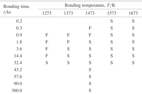
With some combinations of bonding temperature and time, solid state diffusion bonding experiment fails to obtain joints of Si3N4. The bondability at each employed bonding
condition are listed in Table 1, in which ‘‘S’’ means that the bonding at the condition succeeds, while ‘‘F’’ means that it fails. In order to obtain sound joints of Si3N4 using
vanadium insert, the bonding time of 32.4 ks, 3.6 ks, and 1.8 ks or longer is required for bonding at 1273 K, 1373 K, and 1473 K, respectively. At the bonding temperatures of 1573 K and above, very short bonding time of 0.2 ks is enough to obtain sound joints. This result indicates that longer time is required for bonding at lower temperatures. Thus, the formation kinetics of the interfacial microstructure has been investigated in relation with the bonding temper-ature and time.
3.2 Interfacial Microstructures of Si3N4/V Joints
The interfacial microstructures of Si3N4/V joints bonded
at low temperatures of 1273 K, 1373 K and 1473 K appear different from those at high temperatures of 1573 K and 1673 K. The interfacial microstructures at 1473 K and 1673 K are described in the following, which represent the structures at low- and high-temperature bonding conditions, respec-tively.
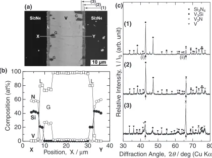
Figure 1 shows the interfacial microstructure of a joint bonded at 1473 K for 3.6 ks. Figure 1(a) is an SEM micrograph of the interface. The dark regions on the
left-and the right-side-end of the micrograph are Si3N4. The
bright particles appearing in the Si3N4are the WSi2sintering
agents. The bright region on the center is vanadium. Defects such as voids and cracks are scarcely observed at the interface. Two types of reaction products are observed between Si3N4 and vanadium. One is formed as a 1.87mm
-thick layer, on which ‘‘L’’ is marked, between Si3N4 and
vanadium. The boundary between Si3N4 and the L-phase is
remaining smooth. The other reaction product is formed as grains, on which ‘‘G’’ is marked, in contact with the vanadium and the layered reaction product. Figure 1(b) shows the elemental distribution profile along the line from X to Y depicted in Fig. 1(a). The L-phase consists of approximately 80 at% V and 20 at% Si with very low content of nitrogen. Referring to the V-Si binary phase diagram,17) the composition corresponds to V3Si. On the other hand, the
G-phase consists of approximately 74 at% V and 26 at% N with very low content of silicon. The V-N binary phase diagram18)suggests that the composition corresponds to V2N.
Figure 1(c) shows a series of X-ray diffraction patterns which correspond to the positions (1), (2) and (3) depicted on the top of Fig. 1(a). The specimen was cut at one side of the Si3N4in
the vicinity of its interface and ground down carefully about 1mmfor each XRD measurement. Each reaction product and its arrangement were identified by the position of each X-ray diffraction peak and the alteration of its relative intensity. All three patterns in Fig. 1(c) are identified as superimposition of Si3N4,19) V3Si,20) V2N21) and V.22) The appearance of all
existing phases in every XRD pattern is due to the detection depth of the diffracted X-ray and the experimental error in polishing flat and parallel to the interface. However, the alteration of the relative intensity appears clearly to the peaks at 42.83 and 66.13, which are marked with arrows (i) and (ii), respectively. The peak (i) corresponds only to the 210 plane of V3Si. Compared with pattern (1), this peak keeps its
intensity in pattern (2) and then it is significantly weakened in pattern (3). The peak (ii), on the other hand, corresponds to the 300 plane of V2N. The relative intensity of the 300 peak
of V2N does not fit the standard diffraction pattern21)
indicating that the 100 plane of V2N is oriented parallel to
the joint interface. Although there is no peak which solely corresponds to V2N, this orientation of V2N clearly suggests
its existence at the interface by the peak (ii). This peak is intensified in pattern (2) and is more intensified in pattern (3). This result agrees well with the EPMA analysis result depicted in Fig. 1(b). Combining the results of SEM, EPMA and XRD, the L-phase and the G-phase are identified as V3Si
and V2N, respectively. Therefore, the apparent phase
sequence is finally identified as Si3N4/V3Si/V+V2N/V.
The interfacial structure of the joints bonded in other conditions of bonding time were also analyzed in the same method. Figure 2 shows a series of SEM micrographs, which reveal four typical stages of interfacial microstructures bonded at 1473 K for different bonding time, with the result of phase identification. The bonding times for the joints depicted in Figs. 2(a), (b), (c) and (d) are 3.6 ks, 57.6 ks, 90.0 ks and 360.0 ks, respectively. In the first stage shown in Fig. 2(a), a layer of V3Si adjacent to Si3N4and grains of V2N
in contact with V3Si and V are formed. In the second stage
[image:2.595.47.291.93.255.2]shown in Fig. 2(b), V5Si3N1X14,23,24) is formed as a layer
Table 1 Success-and-failure diagram of the Si3N4/V/Si3N4 bonding experiment.
Bonding time, Bonding temperature,T/K
t/ks 1273 1373 1473 1573 1673
0.2 S S
0.3 F S S
0.9 F F F S S
1.8 F F S S S
3.6 F S S S S
14.4 F S S S S
32.4 S S S S S
43.2 S
57.6 S
90.0 S
between Si3N4 and V3Si. The Si3N4/V5Si3N1X interface becomes rough. The V2N grains grow and contact with grains
which has grown from the opposite side of the foil. Thus, the phase sequence observed in this stage is described as Si3N4/
V5Si3N1X/V3Si/V+V2N. In the third stage shown in Fig.
2(c), the V phase is annihilated. The central part of the foil is replaced with V2N, which has become a layer. The
V5Si3N1X layer grows depredating the V3Si layer. As the
result, the thickness of the V3Si layer decreases. The
V5Si3N1X layer contains large amount of voids, which appear with round-shaped dark contrast in the micrographs. Especially, large-sized voids are concentrated in the vicinity of the Si3N4/V5Si3N1X interface, as indicated with white arrows in Fig. 2(c). These voids are considered to be N2gas
phase, which is generated by the decrease of nitrogen solubility in the V5Si3N1X during cooling. Thus, the phase sequence observed in this stage is described as Si3N4/
V5Si3N1X/V3Si/V2N. In the fourth stage shown in Fig.
2(d), the V3Si layer is annihilated. Thus, the V5Si3N1Xlayer contacts with the V2N layer. At the V5Si3N1X/V2N
inter-face, VN is newly formed as grains. The phase sequence observed in this stage is described as Si3N4/V5Si3N1X/ V2N+VN/V2N.
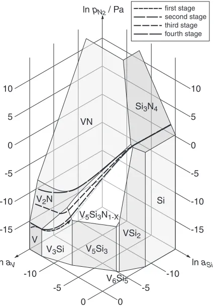
The phase sequence observed at each stage of interfacial structure is verified with available V-Si-N ternary phase diagram.25) Although the phase diagram presents only two isothermal sections at 1273 K and 1773 K, most of the observed phase sequences are consistent with the isothermal
section at 1273 K except in the following two points. One is the Si3N4/V3Si interface, which is observed in the first stage
of the evolution of the interfacial microstructure. The interface requires a V5Si3N1X layer to exist between Si3N4
and V3Si, which is achieved in the second stage, to
equilibrate thermodynamically. Therefore, the Si3N4/V3Si
interface is considered to be in a metastable state, which is observed only in the earliest stage of the interfacial reaction. The other point is the V5Si3N1X/VN interface, which is observed at interfaces in the fourth stage. The thermody-namic state of the V5Si3N1X/VN interface was investigated by chemical state of the constituent elements in each phase, which is calculated standing on the thermodynamic data25) and phase diagrams.17,18,25) Figure 3 proposes the V-Si-N ternary chemical potential diagram at 1473 K, in which V5Si3N1Xis allowed to coexist with VN. This result agrees well with another V-Si-N ternary phase diagram presented by Andruszkiewicz and Horyn´.24)The phase sequences observed in Fig. 2, except the metastable first stage, are compatibly explained with the dashed lines drawn on Fig. 3.
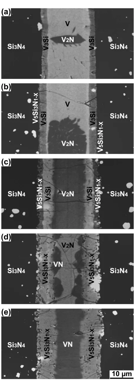
The interfacial microstructure formed at 1573 K and above appears different in early stages of the evolution in the interfacial microstructure from that formed at low-temper-atures. Figure 4 shows a series of SEM micrographs, which reveal five typical stages of interfacial microstructures bonded at 1673 K for different bonding time, with the result of phase identification. The bonding times for the joints depicted in Figs. 4(a), (b), (c), (d) and (e) are 0.9 ks, 1.8 ks,
30
40
50
60
70
80
Diffraction Angle, 2
θ
/ deg (Cu K
α
)
Relativ
e Intensity
,
I / I
0
(arb
. unit)
(c)
(1)
(2)
(3)
Si3N4
V3Si
V2N
V
(i) (ii)
0
10
20
30
40
0
20
40
60
80
100
V
N
Si
Position, X /
µ
m
Composition (at%)
X
Y
L
L
G
(b)
L L
G
G
G
(3) (2)
(1)
(a)
[image:3.595.86.506.76.389.2]3.6 ks, 14.4 ks and 32.4 ks, respectively. In the first stage shown in Fig. 4(a), a layer of V3Si adjacent to Si3N4 and
grains of V2N inside the V are formed. The difference from
the microstructure formed at low-temperatures is that the V2N grains are prohibited to contact with the V3Si layer.
Thus, the phase sequence observed in this stage is described as Si3N4/V3Si/V/V+V2N. The mechanism to prohibit the
V2N grains from contacting the V3Si layer is discussed in the
next paragraph. In the second stage shown in Fig. 4(b), a layer of V5Si3N1X is formed between Si3N4and V3Si. The
V2N grains grow larger still evading contact with the V3Si
layer. The phase sequence observed in this stage is described as Si3N4/V5Si3N1X/V3Si/V/V+V2N. In the third stage
shown in Fig. 4(c), the V is annihilated. The V2N becomes a
layer and finally contacts with the V3Si layer. At this and the
later stages, the interfacial microstructure becomes the same to each corresponding stage at low-temperatures as shown in Figs. 2(c) and (d). The phase sequence observed in the third and the fourth stages are described as Si3N4/V5Si3N1X/ V3Si/V2N and Si3N4/V5Si3N1X/V2N+VN/V2N,
respec-tively. In the fifth stage shown in Fig. 4(e), the V2N layer is
annihilated. Therefore, only V5Si3N1X and VN remain chemically stable in the final stage. The phase sequence observed at this stage is described as Si3N4/V5Si3N1X/VN. The V2N grains are prohibited to contact with the V3Si
layer in early stages of high bonding temperatures. The mechanism is investigated from the nature of the vanadium lying adjacent to the V3Si layer. Figure 5 shows the detailed
composition profile of silicon across the interface bonded at 1673 K for 0.3 ks in comparison with that bonded at 1473 K, 1.8 ks. Both bonding conditions form the V3Si layer of the
same thickness adjacent to Si3N4, which corresponds to the
Fig. 2 Four representative stages of the interfacial structure bonded at 1473 K. The bonding time for each joint is (a) 3.6 ks, (b) 57.6 ks, (c) 90.0 ks and (d) 360.0 ks, respectively.
10
5
0
-5
-10
-15
0 -5 -10
10
5
0
-5
-10
-15
0 -5
-10
lnaV lnaSi
lnpN2 / Pa first stage second stage third stage fourth stage
VN
V2N
V
V3Si V5Si3
V6Si5 VSi2
Si Si3N4
V5Si3N1-X
[image:4.595.56.284.63.683.2] [image:4.595.322.535.72.378.2]first stage of the evolution in the interfacial microstructure. A 0.8mmthick zone in the vanadium adjacent to the V3Si layer
containing approximately 4 at% of silicon is detected in the joint bonded at 1673 K. The diffusion zone of silicon in the vanadium, which is named as the V(Si) zone in the following, is not formed at low-temperature conditions, but only at high-temperature conditions. The composition of V-4 at%Si corresponds to the solubility limit of silicon in vanadium at 1673 K.17)The V-Si-N ternary phase diagram24)suggests that the vanadium saturated with silicon scarcely dissolves nitrogen and that V2N cannot coexist with such highly
silicon-dissolved vanadium. Therefore, V2N is formed inside
the vanadium in which silicon is not dissolved. In other words, the V(Si) zone prohibits the V2N grains to contact
with the V3Si layer. Therefore, the phase sequence observed
at the first and the second stage at 1673 K should be corrected as Si3N4/V3Si/V(Si)/V+V2N and Si3N4/V5Si3N1X/V3Si/
V(Si)/V+V2N, respectively. This result implies that the
interfacial energy of the V3Si/V is reduced by the formation
of the V(Si) zone to a level lower than that of the V3Si/V2N.
Figure 6 shows the V-Si-N ternary chemical potential diagram at 1673 K. The phase sequences observed in Fig. 4, except the metastable first stage, are consistent with the dashed lines drawn on Fig. 6.
Schuster et al.14)has described the phase sequence of the Si3N4/V system at 1273 K to be Si3N4/V2N/V3Si
(V5Si3N1X)/V, which is completely different from the present result. Their prediction stands on the assumption that the interfacial reaction proceeds by the diffusion of silicon from Si3N4to the metal to form metal silicide followed by the
reaction of the metal with the free nitrogen to binary metal nitrides on the Si3N4 side. Although the V(Si) zone is
observed at high-temperatures, the present result at the earliest stage of interfacial reaction showing a V3Si layer
adjacent to Si3N4 strongly suggests that the growth of the
silicide layers is controlled by diffusion of vanadium instead of silicon through the silicide layers, as depicted on Figs. 2 and 6 with arrows on the phase sequences of the first stages. This conclusion is also derived from the morphology of the V3Si/V+V2N interface which is observed in early stages of
low-temperature bonding condition. The V3Si layer has two
Fig. 4 Five representative stages of the interfacial structure bonded at 1673 K. The bonding time for each joint is (a) 0.9 ks, (b) 1.8 ks, (c) 3.6 ks, (d) 14.4 ks and (e) 32.4 ks, respectively.
0 1 2 3 4 5 6 7
0 10 20 30 40 50
1473 K, 1.8 ks 1673 K, 0.3 ks
Position, x / µm
Composition of Silicon,
CSi
(at%)
Si3N4
V3Si
V(Si) V
V
(high temperature) (low temperature)
[image:5.595.54.285.59.706.2] [image:5.595.309.544.75.249.2]different interfaces on the metal side. One is the interface with the V and the other is that with the V2N grains. Although
two different phases contact with the V3Si layer, the
thickness of the layer does not appear different by the difference of the contacting phases. Furthermore, the V3Si
layer grows without embedding V2N grains at their original
positions. This fact indicates that the growth front of the V3Si
layer is not located on the metal side but on the Si3N4side of
the layer. It is important to understand the growth front correctly, because it determines the element dominating the reaction behavior at the interface.
3.3 Growth Behavior of the Reaction Products
In every bonding condition employed in the present study, only V3Si, V5Si3N1X, V2N and VN are formed at the
interfaces. V3Si and V5Si3N1X appear as layers from their initial state, while V2N and VN appear as grains at their
rudiment and then grow to form a layer. In order to estimate the amount of formed grains of V2N and VN, a representative
size of each phase,wi, was defined as
wi¼Ai=2li; ð1Þ
whereAiis the observed total area of each phase andliis the observed length of the interface. This parameter keeps compatibility with the thickness, the size parameter when each phase achieves the formation of its layer.
The increase and decrease behavior in the thickness of each reaction product interacts with each other. Figure 7 shows the growth behavior of each reaction product at
1473 K. The representative size and the thickness of each reaction product are plotted as a function of the square root of bonding time, t1=2. It is clearly shown that V3Si, V2N and
V5Si3N1X grow proportionately with the square root of bonding time, obeying the parabolic law, in its initial stage of growth. Only V3Si appears without showing any latency
period. The thickness of the V3Si layer increases until the
V5Si3N1Xlayer is formed. The formation and growth of the V5Si3N1Xlayer forces the V3Si layer annihilate. The growth
rate of the V5Si3N1X layer is retained until it comes into contact with the V2N by the annihilation of the V3Si layer.
Then, the growth is slowed down. The V2N grains grow until
the grains grown from both sides of the foil contact to each other. It keeps its representative size of 5.65mmuntil the VN grains are formed. The VN grows reducing the thickness of the V2N layer. Figure 8 shows the growth behavior of each
reaction product at 1673 K. It is clearly noticed that every reaction product grows obeying the parabolic law in its initial stage of growth also at this temperature. The V3Si layer
increases its thickness until the V5Si3N1Xlayer is formed. In contrast with the behavior at low-temperatures, the layer does not decrease its thickness by the formation of the V5Si3N1X layer, keeping its thickness of 3.55mmuntil the V3Si layer
first stage second stage third stage fourth stage fifth stage
VN
V2N
V
V3Si V5Si3 VSi2
Si Si3N4
V5Si3N1-X
V6Si5 10
5
0
-5
-10
-15
0 -5 -10
10
5
0
-5
-10
-15
0 -5
-10
lnaV lnaSi
lnpN2 / Pa
Fig. 6 Chemical potential diagram of V-Si-N ternary system at 1673 K. The five types of dashed lines depict the phase sequences observed at five different stages of the joint interfaces shown in Fig. 4.
V3Si V5Si3N1-X V2N VN
0 200 400 600
0 2 4 6 8 10
Square Root of Bonding Time,t1/2 / s1/2
Representativ
e Siz
e and
Thic
kness
of Each Reaction Product,
wi
/
µ
m
Fig. 7 Growth behavior of each reaction product at 1473 K.
0 100 200
0 2 4 6 8 10
Square Root of Bonding Time,t1/2 / s1/2
Representativ
e Siz
e
and
Thic
k
ness
of Each Reaction Product,
wi
/
µ
m V3Si
V5Si3N1-X
V2N
VN
[image:6.595.64.278.71.377.2] [image:6.595.314.538.75.253.2] [image:6.595.316.535.594.767.2]contacts with the V2N layer. The formation of the V3Si/V2N
interface, which indicates the annihilation of the V phase, also stops the parabolic growth of the V2N. The V2N layer
maintains its thickness of 6.04mm until the VN grains are formed. The annihilation of the V3Si layer results in the
suppression of the growth of the V5Si3N1X layer. On the other hand, the annihilation of the V2N layer stops the growth
of the VN. The interaction of the growth behavior of each reaction product is summarized as follows: the V3Si layer
stops its parabolic growth when the V5Si3N1X layer is formed. The reduction in its thickness starts when it contacts to the V2N. The V5Si3N1X layer slows down its growth by contacting to the V2N, which corresponds to the annihilation
of the V3Si layer. The V2N stops its parabolic growth when
the contacting to the V3Si layer and the contacting of the
grains grown from both sides each other are both achieved. The reduction in its representative size starts by the formation of the VN grains. The VN stops its parabolic growth when the V2N is annihilated.
The change in the thickness of the V3Si layer is observed
to be sensitively affected by the behavior of the V2N phase.
As discussed in the last section, whether the V2N contacts
with the V3Si layer is determined by the formation of a thin
V(Si) zone at the V3Si/V interface. Since silicon can diffuse
into vanadium from the beginning of the bonding treatment at high-temperature conditions, the V(Si) zone can affect the growth behavior of the V3Si layer even in its initial stage of
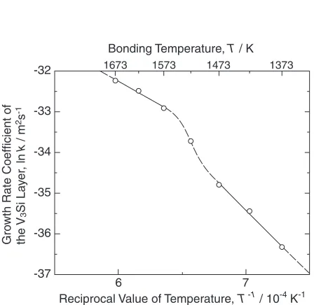
parabolic growth. Figure 9 shows the dependence of the growth rate coefficient of the V3Si layer,k, on the bonding
temperature regarding the Arrhenius-type function
lnk¼lnk0Q=RT; ð2Þ
wherek0 is the pre-exponential factor for the growth rate of
the V3Si layer, Qis the apparent activation energy for the
growth of the V3Si layer,Ris the gas constant andT is the
bonding temperature. The dependence of the growth rate on the bonding temperature for the low-temperature bonding condition appears with different line from that for the high-temperature bonding condition, revealing a transition-tem-perature range between 1473 K and 1573 K. The interfacial microstructure of the joints bonded at the temperatures in this range shows that the V2N grains are formed off the V3Si layer
even at 1498 K. This result indicates that the V(Si) zone starts its formation at the onset temperature of the transition observed in Fig. 9. The values ofk0andQfor the low- and the
high-temperature bonding condition calculated from Fig. 9 are listed in Table 2. The activation energy for the growth of the V3Si layer at high-temperature bonding condition appears
lower than that at low-temperature bonding condition. This result suggests that the formation of the V(Si) zone adjacent to V3Si reduces the activation energy of the growth of the
V3Si layer. As discussed in the previous section, the growth
of the V3Si layer is controlled by the diffusion of vanadium
through the layer, and the V(Si) zone reduces the interfacial energy of the V3Si/V phase boundary to a level lower than
that of the V3Si/V2N. These results support the consideration
that the V(Si) zone improves the diffusion of vanadium in the V3Si layer by reducing the activation energy for dissolution
of vanadium into V3Si. Therefore, the apparent activation
energy for the growth of the V3Si layer corresponds to that
for the dissolution of vanadium into the V3Si layer.
Figures 7 and 8 indicate that the V3Si layer grows up to
6.70mmbefore the V5Si3N1Xlayer is formed at the bonding temperature of 1473 K, while it does up to 3.55mmat 1673 K. This result indicates that the Si3N4/V3Si interface is more
stable at lower temperatures. Since the Si3N4/V3Si interface
is thermodynamically metastable, sufficient amount of vanadium is supplied to the interface to form V3Si adjacent
to Si3N4 in the first stage of interfacial reaction. Therefore,
the formation of the V5Si3N1X layer starts when the diffusion flux of vanadium in the V3Si layer is reduced
below a certain level by increasing the thickness of the V3Si
layer. The diffusion flux of vanadium through the V3Si layer,
JV, is determined regarding to the Fick’s first law:
JV¼ DVð@CV=@xÞ; ð3Þ
where DV and @CV=@x are the diffusion coefficient of vanadium through V3Si and the spatial composition gradient
of vanadium in the V3Si layer, respectively. As shown in Fig.
1(b), however, the composition of vanadium in the V3Si layer
is almost uniform. Thus, the diffusion cannot be driven by the composition gradient. Since the diffusion of an element is caused by the gradient of the chemical potential, to replace the composition,CV, with the activity of vanadium,aV, will
6 7
Reciprocal Value of Temperature,T -1 / 10-4 K-1 -37
-36 -35 -34 -33 -32
Gro
wth Rate Coefficient of
the V
3
Si La
y
e
r,
ln
k
/ m
2s
-1
1673 1573 1473 1373
Bonding Temperature, T / K
[image:7.595.58.282.453.671.2]Fig. 9 Arrhenius plot of the growth rate coefficient of the V3Si layer.
Table 2 A list of the pre-exponential factor of the growth rate and the apparent activation energy for the growth of the V3Si layer at each temperature range.
Temperature range, Pre-exponential factor for the Apparent activation energy for
T/K growth rate,k0/m2s1 the growth,Q/kJ mol1
1373-1473 1:30106 260
[image:7.595.45.551.734.786.2]explain the diffusion more correctly. Thus, the equation (3) can be modified as
JV¼ DV
@aV
@x ¼ DV
@expðV=RTÞ @x
¼ DV
RTexp
V
RT
@
V
@x ð4Þ
in the isothermal condition, where V is the chemical potential of vanadium. The eq. (4) indicates that the diffusion flux depends proportionately on the spatial gradient of the chemical potential of vanadium, @V=@x. The value of @V=@xwas roughly estimated by dividing the difference in the chemical potential of vanadium at the Si3N4/V3Si and the
V3Si/V+V2N interfaces, V, with the observed critical thickness of the V3Si layer for the formation of the
V5Si3N1X layer, wV3Si
. The calculation of V=wV3Si
for the bonding temperatures of 1473 K and 1673 K deduces
3:36109 and 3:31109J mol1m1, respectively. Both values appears almost the same. This result suggests that the V5Si3N1X layer is formed to establish the local equilibrium at the interface with Si3N4 when the spatial
gradient of the chemical potential of vanadium in the V3Si
layer decreases to a value below 3:3109J mol1m1,
being independent on the bonding temperature, by increasing the thickness of the V3Si layer.
3.4 Joint Strength and Fracture
The fracture strength of the joints changes depending on the bonding time. Figures 10(a) and (b) depict the depend-ence of the fracture strength on the bonding time for the joints bonded at 1473 K and 1673 K, respectively. The fracture strength of the joints bonded at 1473 K is improved until the bonding time of 5.2 ks, at which the maximum average-strength of 67 MPa is obtained. Referring to Fig. 7, the
bonding condition of 1473 K for 5.2 ks corresponds to the formation of a 2.0mm-thick V3Si layer adjacent to Si3N4. The
prolonged bonding time over 5.2 ks gradually reduces the fracture strength down to 42 MPa. The fracture strength of the joints bonded at 1673 K is increased until the bonding time of 0.4 ks, at which the maximum average-strength of 94 MPa is obtained. The bonding condition of 1673 K for 0.4 ks corresponds to the formation of a 2.0mm-thick V3Si
layer adjacent to Si3N4. The prolonged bonding time over
[image:8.595.92.282.100.153.2]0.4 ks gradually reduces the fracture strength down to 43 MPa and significantly expands the scatter in the data.
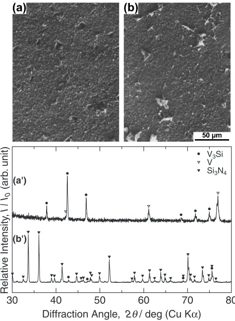
Figure 11 shows a pair of SEM micrographs and corresponding XRD patterns taken from both sides of the fracture surfaces of a joint bonded at 1473 K for 3.6 ks, at which the strong joint of 64 MPa was obtained. Both fracture surfaces appear microscopically flat, indicating that the fracture occurs at the interface in a brittle mode. The side on which the vanadium foil is remaining is named the ‘‘V side’’, while the other side is named as the ‘‘Si3N4side’’. On the
V-side surface (Fig. 11(a)), only V3Si is detected, on which pits
are dispersed. The XRD pattern taken from the V side (Fig. 11(a’)), in which only V3Si and V are detected, agrees with
this analysis result. Corresponding to the pits on the V-side surface, sharp-edged particles of V3Si are observed on the
Si3N4-side surface (Fig. 11(b)). In agreement with the
EPMA, the XRD pattern taken from the Si3N4 side (Fig.
11(b’)) indicates that Si3N4and small amount of V3Si exists
on the surface. Based on these results, the fracture is
0 50 100 150 200
Square Root of Bonding Time,t1/2 / s1/2 0
20 40 60 80 100
F
racture Strength,
σf
/ MP
a
1673 K
0 100 200 300 400 500 600
Square Root of Bonding Time,t1/2 / s1/2 0
20 40 60 80 100
F
racture Strength,
σf
/ MP
a
1473 K
(a)
[image:8.595.308.545.424.748.2](b)
Fig. 10 Dependence of the fracture strength of the Si3N4/V joints on the bonding time. (a) bonded at 1473 K, (b) at 1673 K.
30 40 50 60 70 80
Diffraction Angle, 2θ / deg (Cu Kα)
Relativ
e Intensity
,
I / I
0
(arb
. unit)
V3Si
V Si3N4
(a')
(b')
[image:8.595.57.278.510.758.2]determined to occur mainly at the Si3N4/V3Si interface and
partly inside the V3Si layer. Figure 12 shows a pair of XRD
patterns taken from a joint bonded at 1473 K for 360.0 ks, at which the joint strength is reduced to 43 MPa. The XRD pattern taken from the V side (Fig. 12(a)) indicates the existence of Si3N4 and V5Si3N1X on the surface. However, Si3N4 is observed only at the areas where the insert foil has
been chipped off. Thus, the peaks of Si3N4in the pattern are
originated from the counterpart of the joint. On the other hand, Si3N4 and V5Si3N1Xare detected in the XRD pattern taken from the Si3N4side (Fig. 12(b)). Therefore, the fracture
is determined to occur at the V5Si3N1Xin the vicinity of the Si3N4/V5Si3N1X interface. The analysis of the fractured surfaces of the joints bonded at 1673 K results in the same conclusion as that of 1473 K: the high-strength joints are fractured at the Si3N4/V3Si interface and the joints bonded
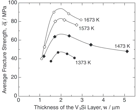
with the prolonged bonding time are fractured at the V5Si3N1Xin the vicinity of the Si3N4/V5Si3N1Xinterface. The maximum fracture strength is achieved when the thickness of the V3Si layer is 2.0mm. Itoet al.,15)also, have
reported the formation of a 2mm-thick V3Si layer adjacent to
Si3N4at the optimum bonding condition. Figure 13 shows the
relation between the average fracture strength and the thickness of the V3Si layer. In every bonding temperature
between 1373 K and 1673 K, the maximum fracture strength is obtained when the thickness of the V3Si layer is 2.0mm,
regardless of the bonding temperature. In addition, the higher bonding temperature leads to the higher maximum fracture strength. The improvement and deterioration behavior of the fracture strength without the formation of the V5Si3N1X layer is considered to be the competition process of the following two factors. One is the improvement in the fracture strength, explained by the chemical-bond formation process in atomic scale at the Si3N4/V contact area and by the plastic
deformation of the vanadium foil to expand the contact area. Since the yield strength of vanadium is lower at higher temperatures, the fraction of contact area in atomic scale becomes larger at higher temperatures to increase the maximum fracture strength. The other factor is the deterio-ration of the fracture strength, explained by the magnitude of the thermal residual stress as a function of the thickness of the
V3Si layer, especially that concentrated at the edge of the
bond interface. Although the mismatch of the thermal expansion coefficient for the Si3N4/V3Si interface is
report-ed,14)the yield strength and the elastic modulus of V3Si as
functions of the temperature are not found in the literature, which are necessary for the estimation of the magnitude of the thermal residual stress.
The V5Si3N1Xlayer is formed at the interface of the joints bonded with the prolonged bonding time. The average fracture strength of such joints converges to a value of approximately 42 MPa, being insensitive to the bonding temperature. The fracture of such joints occurs at the V5Si3N1Xin the vicinity of the Si3N4/V5Si3N1Xinterface, which corresponds to the position where the segregation of large-sized voids is observed as shown in Figs. 2 and 4. Therefore, the fracture is considered to occur by crack propagation connecting these voids. Since the voids are formed by the N2 gas generated during cooling, the fracture
property of the joints at this state of interfacial microstructure is sensitive to the behavior of nitrogen. For example, regarding to Figs. 7, 8 and 10, the scatter of the fracture strength expands when the V5Si3N1Xcontacts with the V2N.
This change in the microstructure will affect the formation and segregation behavior of the voids.
The results described in this section indicates that the formation of the 2.0mm-thick V3Si layer adjacent to Si3N4is
required to obtain the maximum average strength of the Si3N4/V joints. In addition, higher bonding temperature
leads to the higher maximum strength. However, the Si3N4/
V3Si interface is a metastable state. The V3Si layer is allowed
to grow up to 3.55mmat the bonding temperature of 1673 K, as described in Fig. 8, and will be lesser at higher temper-atures. Therefore, the bonding temperatures which does not allow the V3Si layer to grow thicker than 2.0mm is
considered to be inadequate.
4. Summary
Si3N4 was bonded to vanadium foils by solid state
diffusion bonding. The interfacial microstructure and
reac-30 40 50 60 70 80
Diffraction Angle, 2θ / deg (Cu Kα)
Relativ
e Intensity
,
I / I
0
(arb
. unit)
V5Si3N1-X
Si3N4 (a)
[image:9.595.56.281.70.239.2](b)
Fig. 12 XRD patterns taken from both sides of the fracture surfaces of a joint bonded at 1473 K for 360.0 ks. (a) were taken from the V side, (b) from the Si3N4side.
1673 K
1573 K
1473 K
1373 K
0 1 2 3 4 5
Thickness of the V3Si Layer,w / µm 0
20 40 60 80 100
A
v
er
age F
racture Strength,
σf
/ MP
[image:9.595.314.538.75.256.2]a
tion kinetics were analyzed in detail by means of SEM, EPMA and XRD. The strength of the joints was estimated by a shear fracture test. The following points were clarified.
(1) The interfacial phase sequence of the Si3N4/V joints
bonded at 1473 K and below changes revealing four stages of transition as follows: (i) Si3N4/V3Si/
V+V2N/V, (ii) Si3N4/V5Si3N1X/V3Si/V+V2N, (iii)
Si3N4/V5Si3N1X/V3Si/V2N, and (iv) Si3N4/
V5Si3N1X/V2N+VN/V2N. At the bonding
temper-atures of 1498 K and higher, the V2N grains are
prohibited to contact with the V3Si layer by the V(Si)
zone. At these temperatures, five stages of transition in the interfacial phase sequence are observed as follows: (i) Si3N4/V3Si/V(Si)/V+V2N, (ii) Si3N4/V5Si3N1X/ V3Si/V(Si)/V+V2N, (iii) Si3N4/V5Si3N1X/V3Si/
V2N, (iv) Si3N4/V5Si3N1X/V2N+VN/V2N, and (v)
Si3N4/V5Si3N1X/VN. The Si3N4/V3Si interface
ob-served in the first stage is metastable. These phase sequences except the metastable interface are success-fully expressed on the proposed chemical potential diagram.
(2) The growth front of the V3Si layer is located on the
Si3N4 side, indicating that the diffusion of vanadium
through the V3Si layer dominates the growth of the
layer.
(3) The increase and decrease behavior in the thickness of each reaction product interacts with each other. Every reaction product grows obeying the parabolic law in its initial stage of growth. The pre-exponential growth constant and the activation energy for the growth of the V3Si layer appear different between the high- and
low-temperature bonding conditions. The formation of the V5Si3N1Xlayer starts when the spatial gradient of the chemical potential of vanadium in the V3Si layer
decreases to a value below3:3109J mol1m1 by
the growth of the V3Si layer.
(4) The maximum fracture strength is achieved when the thickness of the V3Si layer is 2.0mm. The higher
bonding temperature leads to the higher maximum fracture strength. The fracture of the joints bonded at this condition occurs in a brittle mode mainly at the Si3N4/V3Si interface and partly inside the V3Si layer.
The prolonged bonding time gradually reduces the fracture strength down to 42 MPa. The joints are fractured at the V5Si3N1X in the vicinity of the Si3N4/V5Si3N1X interface by crack propagation con-necting the voids.
Acknowledgements
The authors express their gratitude to Dr. Harumi Yokokawa, National Institute of Materials and Chemistry, for the discussion on the reaction phenomena between ceramics and metals from thermodynamical point of view.
REFERENCES
1) R. F. Mattas and M. C. Billone: J. Nucl. Mater.233-237(1996) 72-81. 2) D. L. Smith, M. C. Billone, S. Majumdar, R. F. Mattas and D.-K. Sze: J.
Nucl. Mater.258-263(1998) 65-73.
3) D. L. Smith, M. C. Billone and K. Natesan: Int. J. Refractory Met. & Hard Mater.18(2000) 213-224.
4) D. L. Smith, J.-H. Park, I. Lyublinski, V. Evtikhin, A. Perujo, H. Glassbrenner, T. Terai and S. Zinkle: Fusion Eng. and Design61-62
(2002) 629-641.
5) Y. Nemoto, K. Ueda, M. Satou, A. Hasegawa and K. Abe: J. Nucl. Mater.258-263(1998) 1517-1522.
6) R. Yasuda, M. Satou, A. Hasegawa and K. Abe: J. Nucl. Mater. 258-263(1998) 1528-1532.
7) F. W. Clinard, Jr., G. F. Hurley and R. W. Klaffky: Res Mechanica8
(1983) 207-234.
8) F. L. Riley: ENCYCLOPEDIA OF MATERIALS SCIENCE AND
ENGINEERING, ed. by M. B. Bever, (Pergamon Press, London, 1986)
Vol. 6, pp. 4412-4415.
9) H. Mori, T. Sakata, H. Yasuda and M. Maeda: J. Vac. Sci. Tech. B12
(1994) 2376-2379.
10) Y. Nakao, K. Nishimoto and K. Saida: Trans. Jpn. Weld. Soc.20(1989) 66-76.
11) Y. Morizono, T. Nakata, M. Nishida and A. Chiba: J. Ceram. Soc. Jpn.
103(1995) 810-815, in Japanese.
12) S. D. Peteves, M. Paulasto, G. Ceccone and V. Stamos: Acta Mater.46
(1998) 2407-2414.
13) P. Lamparter, S. Steeb and A. Gukelberger: High Temperatures-High Pressures3(1971) 727-740.
14) J. C. Schuster, F. Weitzer, J. Bauer and H. Nowotny: Mater. Sci. Eng.
A105/106(1988) 201-206.
15) Y. Ito, K. Kitamura and M. Kanno: J. Mater. Sci.28(1993) 5014-5018. 16) I. Gotman and E. Y. Gutmanas: Acta Metall. Mater.40(1992) Suppl.
S121-S131.
17) Binary Alloy Phase Diagrams, ed. by T. B. Massalski, (American
Society for Metals, Metals Park, Ohio, 1986) pp. 2060-2062.
18) Binary Alloy Phase Diagrams, ed. by T. B. Massalski, (American
Society for Metals, Metals Park, Ohio, 1986) pp. 1656-1659.
19) Powder Diffraction File, JCPDS, 33-1160.
20) Powder Diffraction File, JCPDS, 19-1405.
21) Powder Diffraction File, JCPDS, 32-1413.
22) Powder Diffraction File, JCPDS, 22-1058.
23) Powder Diffraction File, JCPDS, 40-956.
24) R. Andruszkiewicz and R. Horyn´: J. Less-Common Met.124(1986) 205-210.
25) Phase Diagrams of Ternary Boron Nitride and Silicon Nitride Systems,