A Octuple Switching Structure with Code
Independent for Frequency Conversion of High
Performance D/A Converters
Wang liguo, Wang zongmin, and Kong ying
Abstract—A new switching structure for decreasing signal dependent nonlinearity and upconverting in high performance D/A converters is addressed in this paper. The switching which receives a digital data input signal that is defined at data intervals can removing any substantial data dependency from this interaction. The logic circuit controls the switchs to be in one of a normal mode or multi-mixer mode that convert the input digital data signal into a mixed analog signal having a mixer frequency that is higher than the data frequency. Simulation results show that the new switch structure most extend the usable frequency spectrum into fifth to sixth Nyquist zone beyond conventional DACs.
Index Terms—Differential octuple swithing, direct digital modulation, data independent
I. INTRODUCTION
I
N high performance digital-to-analog converters (DAC), noise becomes an ever more limiting consideration as dynamic range increases and/or as minimum detectable sig-nal decrease. One particular source of noise in a mixed digital and analog signal application is effect on critical analog signal paths of the various digital circuit. One com-monly used such critical analog signal path is the switch or steering of analog reference signals by control elements, which are themselves activated by digital control signals. In a physically realizable system, it is impossible to completely isolate these digital control signal from analog signals which they are controlling because of coupling through the analog signal control elements [1], and also because digital circuits consume time-varying power and cause time-varying loading [2], IR drops [3], and charge injection, which in turn cause interactions with the overall signal processing circuit. These effects cause changes in reference signals, supply voltages, bias levels, clock phases, transition phase, and substrate effects that in turn corrupt the desired analog signal being processed. Because of inevitable parasitics and non-ideal circuits, this can cause data dependant loading and spurious coupled signal modulation [4]. In this manner the digital signals add noise and/or distortion to the analog signals.In direct digital modulation systems, the signal is up-converted in digital domain, and the modulated digital is converted into a modulated analog form. In these systems, a digital-to-analog converter (DAC) whose conversion rate is more than the Nyquist rate of the carrier frequency. A
Manuscript received June 23, 2011; revised July 7, 2011. This work was supported by Beijing Microelectronics Tech-Institution(BMTI).
Wang liguo is the postgraduate of Beijing Microelectronics Tech-Institution, No.2. Siyingmen N.Rd Donggaodi Fengtai District,Beijing 100076,China e-mail: [email protected].
[image:1.595.318.535.192.350.2]Wang zongmin and Kong ying are with Beijing Microelectronics Tech-Institution(BMTI).
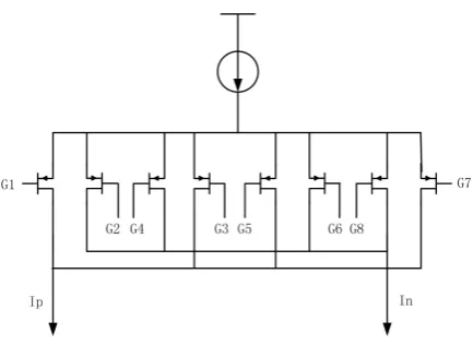
Fig. 1. The structure of octuple switching
wide variety of different electronic device use a system that both converts internal digital signals to analog signals, and then shift the frequency of the resultant analog signal. For example, conventional cell phones often have a digital to analog chip converter chip that converts a digitally processed voice signal into an analog baseband signal for transmission. Before transmission, however, a mixer chip shifts the fre-quency of the baseband signal to a frefre-quency that facilitates transmission.
An effective switching structure, called differential-octuple switching (DOS) is proposed for the oversampling DAC to meet the requirements for direct digital modulation and data independent. Fig.1 is the circuit based on DOS. Section II gives the structure of octuple switching. Section III discusses the theory of switching. Section IV describes the control circuit of switching. Section V contains some conclusions plus some ideas for code independent of glitch. Section VI presents the primary experimental results of the paper and the section VII is the conclusion.
II. DIFFERENTIAL OCTUPLE SWITCH
Fig. 2. General wave of DAC output
separately and the DAC output change only when either of them changes. As a multi-bit DAC, the switchs changed state will produce glitch through the capacitor between gate and drain but those not changed will not impact on output, then the output glitch depend on data patten.
If, however, the switchs act every clock edge or half a clock cycle or a quarter clock cycle, the frequency of this noise will not be in the band of signal but have a certain relationship with the conversion clock frequency. The noise frequency either is as same as the carrier band frequency or twice or four times as high as the carrier band frequency.
This switching is DOC. Fig.1 is the simplified circuit based on DOC. Each switch is controlled by one signal that is come from the logic operation of input data and clock, the switch apparatus has a current source that transmit a current to either one of two differential output nodes Ip and In via one of the eight switches G1-G8. To the end, no more than one of eight switches G1-G8 can be in an “on” state at any single time. For each quarter DAC clock cycle, one of the eight transistors changes their state while the others remain off. The data input to the segment determines whether the current for this segment is re-routed by this switching, thereby changing the differential output current levels, or only routed through a different transistor for an unchanged output.
III. SWITCHING THEORY
According to the sample theorem, as long as we sample fast enough, digital signal x(n) contains all information of analog signal x(t). If we hope to reconstruct x(t) from x(n) perfectly, we can let
g(t) =sin(π∗fs∗t) π∗fs∗t
, x(t) =
∞
X
n=−∞
x(n)∗g(t−nTS)
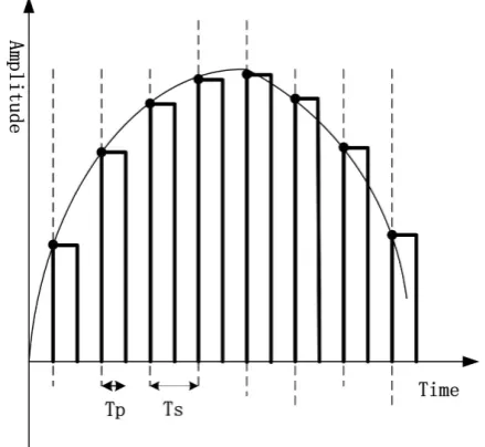
But it is very hard to build an analog circuit that does this. The most practical way of reconstructing the continuous time signal is to simply “hold” the discrete time values that is continued either for full period Ts or a fraction Tp. It is illustrated in Fig.2.
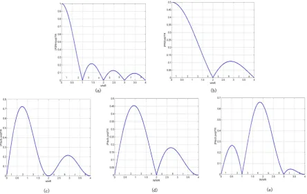
Fig. 3. The time domain wave of switching function (a)zero-order hold pulse. (b)RZ hold pulse. (c)2p2L hold pulse. (d)4p3L hold pulse. (e)4p2L hold pulse
The process of “hold” can be realized through an analog circuit that we can call it switch whose function is the recon-structing. Consider the general case with a rectangular pulse
0 < T p < T s, let the rectangular unit pulse is h(t)=u(t)-u(t-Tp), the time domain signal follows from convolving the Dirac sequence with it. Because of
x(t) =
∞
X
n=−∞
x(n)∗h(t−nTS)
Hp(f) =T psin(π∗f∗Tp) π∗f∗Tp
e−jπ∗f∗Tp then
Xp(f) = T p T s
sin(π∗f∗Tp)
π∗f∗Tp
e−jπ∗f∗Tp ∞
X
n=−∞
X(f− n
T s)
As to a discrete signal x(n), the spectrum Xd(f) is Period-ically spread of spectrum X(f) which is Fourier transform of x(t). So, when we reconstruct the x(t) from x(n), in frequency domain the reconstruction function Hp(f) which we select filters the Xd(f). As follow, we will design the reconstructed function which is realized by DOC and fulfills the reconstruction and upconversion of DAC.
A. Zero-Order Hold Pulse
In the normal DAC mode, the reconstruction function of switch is zero-order hold pulse in Fig.3.(a) We let
PZRH(t) =
1
Y
(0,TR)
(t) =
1 0< t < TR
0 t <0or t > TR
then
PZRH(t) =
1
Y
(0,TR)
(t) =u(t)−u(t−TR)
Laplase transform
L{
1
Y
(0,TR)
(t)}=L{u(t)−u(t−TR)}=
1 s−
1 se
−sTR= 1−e −sTR
s
Fourier transform
F{
1
Y
(0,TR)
(t)}=1−e
−sTR
s |s=jw
F{
1
Y
(0,TR)
(t)}=TR
ejwTR2 −e−jw
TR
2
2jwTR
2
[image:2.595.60.280.55.257.2]Fig. 4. The wave of switching function in frequency domain (a)zero-order hold pulse. (b)RZ hold pulse. (c)2p2L hold pulse. (d)4p3L hold pulse. (e)4p2L hold pulse
PZRH(w) =TR
sin(wTR
2 ) wTR
2
e−jwTR2 =TRSa(wTR 2 )e
−jwTR2
From the figure, we can get whenw=nwr(n∈z, n6= 0),
the sample function have zero point and the envelope of function drop at the speed of -20dB/Decade or -6dB/Octant. In Fig.4.(a), number 1 to 8 is the Nyquist zone, the Nyquist frequency is wR/2 and the spectrum is the most strong at 1 Nyquist zone at which the normal DAC work and is the baseband zone. the amplitude of other zones spectrum is force to get more decreased.
B. Return to Zero Pulse
We can call the return to zero pulse double phase single polar level(RZ) in Fig.3.(b)
PZRH(t) =
1
Y
(0,TR2 ) (t) =
1 0< t < TR
2 0 t <0 or t > TR
2
then
PZRH(t) =
1
Y
(0,TR2 )
(t) =u(t)−u(t−TR
2 )
F{
1
Y
(0,TR2 )
(t)}= 1−e
−sTR2
s |s=jw
F{
1
Y
(0,TR2 )
(t)}=TR 2
ejwTR4 −e−jwTR4
2jwTR
4
e−jwTR4 =PZRH(w)
PZRH(w) =
TR
2
sin(wTR
4 ) wTR
4
e−jwTR4 =TR 2 Sa(w
TR
4 )e
−jwTR4
From the spectrum of the return to zero in Fig.4.(b), we can see that the width of it increases to double times more than the spectrum of zero-order hold PRZ(w) meanwhile the amplitude decrease to one half. So the spectrum amplitude of first Nyquist zone is restrained but the second and third zone is strengthened relative to the PZRH(w).
C. Biphase Bipolar Level Pulse(2p2L)
P2p2L(t) =
1
Y
(0,TR2 ) (t)−
1
Y
(TR2 ,TR)
(t) =
1 0< t < TR
2
−1 TR
2 < t < TR 0 others
then
P2p2L(t) =u(t)−2u(t−
TR
2 ) +u(t−TR)
the wave of time domain is Fig.3.(c), Fourier transform
F{P2p2L(t)} = 1−2e
−sTR2 +e−sTR
s |s=jw=P2p2L(w)
P2p2L(w) = 1−2e
−jwTR2 +e−jwTR
jw =
(1−e−jwTR2 )2
jw
=TR
sin2(wTR4 )
wTR4 e jπ
2−jwTR4
=TRSa(π2wwR)sin(π2wwR)ej
π
2−jw
TR
4
here, letθ=π2ww
R,
d(sin2(θ))
θ |θ=θ0 then we can get when
θ0=π w 2wR
≈1.1655,|P2p2L(w0)|= 0.7264TR
So the spectrum in Fig.4.(c) absolutely restrains the DC signal and restrains the first Nyquist zone spectrum in a large degree, but strengthens the second and third Nyquist zone spectrum especially the second Nyquist zone spectrum is strengthened smoothly. To DAC, the realization can be called upconversion.
D. Quadphase Triple Level Pulse(4p3L) The wave of time domain is Fig.3.(d)
P4p3L(t) =Q
1
(0,TR4 )(t)−
Q1
(0,TR4 )(t−
TR
2 )
=u(t)−u(t−TR
4 )−u(t−
TR
2 )−u(t−3
TR
4 )
F{P4p3L(t)} =1−e
−sTR2 −e−sTR4 +e−3sTR4
s |s=jw
=(es
TR
8 −e−sTR8 )(esTR4 −e−sTR4 )
s e
−3sTR8 | s=jw
=P4p3L(w)
then
P4p3L(w) = T2R
sin(wTR8 )
wTR8 sin(w TR
4 )e
jπ
2−3jwTR8
= TR
2 Sa(π
w
4wR)sin(π
w
2wR)e
jπ
2−3jw
TR
8
The spectrum of Quad-phase triple level pulse in Fig.4.(d) strengthens the second and third Nyquist zone amplitude smoothly more than Biphase Bipolar level pulse. So it can realize the function of upconversion better.
E. Quad-Phase Bipolar Level Pulse(4p2L) The wave of time domain is Fig.3.(e)
P4p2L(t) =u(t)−2u(t−T4R) + 2u(t−T2R)
−2u(t−3TR
4 ) +u(t−TR)
Fourier transform
F{P4p2L(t)} =1+2e
−sTR2 −2e−sTR4 −2e−3sTR4 +e−sTR
s |s=jw
=(e
sTR8
−e−sTR8 )2(esTR4 +e−sTR4 )
s e
−sTR3 | s=jw
=P4p2L(w)
then
P4p2L(w) =TR
sin(wTR8 )
wTR8 sin(w TR
8 )cos(w
TR
4 )e
jπ
2−jw
TR
2
=TRSa(π4ww
R)sin(π
w
4wR)cos(π
w
2wR)e
jπ
[image:4.595.318.535.51.284.2]2−jwTR2 the spectrum of Quad-phase Biphase level is Fig.4.(e) and strengths the fourth and fifth Nyquist zone amplitude spec-trum. So it can realize the function of upconversion higher.
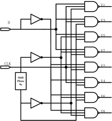
[image:4.595.49.296.198.425.2]Fig. 5. The control circuit of the switching input signal
Fig. 6. The control circuit of the switching input signal
IV. THE CONTROL CIRCUIT OF SWITCHING
The control circuit of switching decides which switch is “on” stale. Because no more than one of eight switches can be “on” state at any single time, for example, if switch G1 is on, and G2-G8 is off. In that case, the current flows to output Ip and the current on output node In is zero. The differential output signal (Ip-In) therefore is +1, when switch G2 is on and others are off. The current therefore flows to the output node In, which produces a differential output signal of -1.
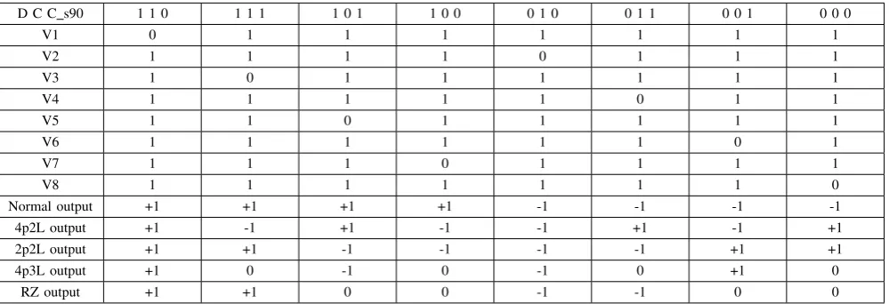
From section III, in this paper, we will introduce five worked modes of DAC. That are separately zero-order hold mode(Normal), return to zero mode(RZ), Biphase Bipo-lar level mode(2p2L), Quad-phase triple level mode(4p3L), Quad-phase Bipolar level mode(4p2L). D is the input data, C is clock and theC s90 is the result that the clock shifts 90 degree. As to the five modes of zero-order normal, 2p2L, 4p2L, RZ and 4p3L. V1-V8 are the result of operation of C,C s90and D, the arithmetic operators is NAND, see the Fig.5.
TABLE I
=THE RESULT OF FIVE DAC MODES
D C C s90 1 1 0 1 1 1 1 0 1 1 0 0 0 1 0 0 1 1 0 0 1 0 0 0
V1 0 1 1 1 1 1 1 1
V2 1 1 1 1 0 1 1 1
V3 1 0 1 1 1 1 1 1
V4 1 1 1 1 1 0 1 1
V5 1 1 0 1 1 1 1 1
V6 1 1 1 1 1 1 0 1
V7 1 1 1 0 1 1 1 1
V8 1 1 1 1 1 1 1 0
Normal output +1 +1 +1 +1 -1 -1 -1 -1
4p2L output +1 -1 +1 -1 -1 +1 -1 +1
2p2L output +1 +1 -1 -1 -1 -1 +1 +1
4p3L output +1 0 -1 0 -1 0 +1 0
RZ output +1 +1 0 0 -1 -1 0 0
and the output result of five modes. Because the operation mode we design is programmable, we select a 3 to 8 encode to produce five control signals which control separately five DAC modes. The output D1 represents Normal mode. D2 represents the 2p2L mode that we only need to let V5 to G6, V6 to G5, V7 to G8, V8 to G7. D3 represents 4p2L mode that we only need to let V3 to G4, V4 to G3, V7 to G8, V8 to G7. D4 represents 4p3L mode that we only need to link V3 and V4, V7 and V8, let V5 to G6, V6 to G5. D5 represents return to zero mode that we only need to link V5 and V6, V7 and V8. See the Fig.6.
V. CODE INDEPENDENT OF GLITCH
While the data do not change in two successive clock cycle, the operation will produce the variational data on the switchs, but do not bring the change on the output. While the data change in two successive clock cycle, the switchs that change accord with data will bring the change on the output.
From this no matter whether the input data change, the output signal complemental change all the way and do not have any relation with the input data. So the glitch which is correlated to the input data is transformed the glitch at a fixed frequency that is four times of the clock, far from the baseband and be filter.
With this scheme, the disturbances to the circuits of this segment (most particularly to the source node of the switches) or adjacent circuits are data-independent, since one transistor turns on and others turns off each quarter clock cycle. This prevents data dependent pumping of any nodes.
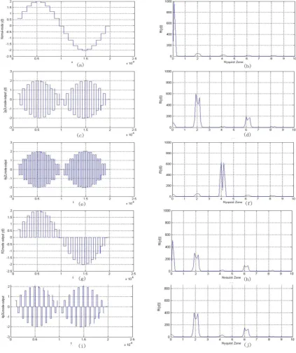
VI. EXPERIMENTAL RESULT
The Matlab simulation result of DOC is illustrated in Fig.7. The input signal is the digital sinusoidal
f(n) =sin(π∗105∗n) + 2
whose frequency is 100Khz and the resolution is 10 bit. A 2048 point FFT is calculated based on the output signal. In Fig.7, the normal mode, (a) is wave of the time domain and we can see that the first Nyquist zone spectrum is strengthened from frequency spectrum (b). In the Fig.7, the Biphase Bipolar level mode(2p2L), (c) is wave of the time
domain and we can see that the spectrum (d) is restrained the first Nyquist zone spectrum in a large degree, but strengthed the second and third Nyquist zone spectrum, so the spectrum is modulated the second and third Nyquist zone. In Fig.7, Quad-phase Bipolar level mode (4p2L), (e) is wave of the time domain and we can see that the spectrum (f) mainly strengthens the fourth and fifth Nyquist zone thus can realize the more high upconversion. In Fig.7, return to zero mode, (g) is wave of the time domain and we can see that the second and third Nyquist zone spectrum is strengthened from frequency spectrum (h) meanwhile the first Nyquist zone spectrum is decrease one half, so the spectrum is modulated the second and third Nyquist zone. In the Fig.7, Quad-phase triple level mode, (i) is wave of the time domain and we can get the second and third Nyquist zone spectrum (j) which is compared with the 2p2L mode is more strengthened, so it can be realization of upconversion.
VII. CONCLUSION
A novel switching structure called differential octuple switch able to overcome the output nonlinearities depend on input data and realized to upconversion is proposed. Through the designed control circuit, it can make the DAC worked at five modes whose functions are modulator and we can select anyone to achieve the upconversion of the output signal.
REFERENCES
[1] A. V. den Bosch, M. A. F. Borremans, M. S. J. Steyaert, and W. Sansen, “A 10-bit 1-GSample/s Nyquist Current-Steering CMOS D/A Con-verter,”IEEE J. Solid-State Circuits, vol. 36, no. 3, pp. 315–324, 2001. [2] G. A. M. V. der Plas, J. Vandenbussche, W. Sansen, M. S. J. Steyaert, and G. G. E. Gielen, “A 14-bit Intrinsic Accuracy Q2 Random Walk CMOS DAC,”IEEE J. Solid-State Circuits, vol. 34, no. 12, pp. 1708– 1718, 1999.
[3] C.-H. Lin, F. M. der Goes, J. R. Westra, J. Mulder, Y. Lin, E. Arslan, E. Ayranci, X. dong Liu, and K. Bult, “A 12 bit 2.9GS/s DAC With IM3¡-60dBc Beyond 1 GHz in 65nm CMOS,” IEEE J. Solid-State Circuits, vol. 44, no. 12, pp. 3285–3293, 2009.
[4] D. A. Mercer, “LOW POWER APPROACHES TO HIGH SPEED CMOS CURRENT STEERING DACS,” IEEE Custom Intergrated Circuits Conference., pp. 153–160, 2006.