A Thesis Submitted for the Degree of PhD at the University of Warwick
http://go.warwick.ac.uk/wrap/35790
This thesis is made available online and is protected by original copyright. Please scroll down to view the document itself.
Capacitive Imaging Technique For
Non-destructive Evaluation (NDE)
By
Xiaokang Yin B.Eng. M.Sc.
Submitted for the degree of
Ph.D. in Engineering
to the
University of Warwick
Describing research conducted in the
School of Engineering
i
Table of Contents
List of Figures ... vi
List of Tables ... xviii
Acknowledgements ... xix
Declaration ... xx
Summary ... xxi
Chapter 1 Introduction ... 1
1.1 Introduction ... 1
1.2 Electrical and magnetic methods of NDE ... 2
1.2.1 Eddy current methods ... 2
1.2.2 Potential drop methods ... 4
1.2.3 Magnetic methods ... 5
1.2.4 Capacitive methods ... 6
1.2.5 Other electromagnetic methods... 8
1.3 A general review on capacitive sensors ... 10
1.4 Objectives of the research and outline of the thesis ... 12
1.5 References ... 16
Chapter 2 The Capacitive Imaging (CI) technique ... 22
2.1 Introduction ... 22
2.2 Capacitive imaging fundamentals ... 22
2.3 General theoretical background ... 25
2.3.1 Maxwell equations ... 25
ii
2.3.3 Electrical properties of specimens under test ... 27
2.3.4 Capacitance ... 29
2.3.5 Calculating capacitance ... 29
2.4 Modes of operation ... 31
2.4.1 The CI probe with a non-conducting specimen under test ... 31
2.4.2 A non-conducting specimen between the CI probe and a grounded substrate ... 32
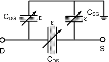
2.4.3 The CI probe with a grounded conducting specimen under test ... 33
2.4.4 The CI probe with a floating conducting specimen under test... 34
2.4.5 Discussions on the modes of operation ... 35
2.5 Measurement method ... 35
2.6 Instrumentation ... 38
2.6.1 Instrumentation description ... 38
2.6.2 Explanatory notes on the instrumentation ... 40
2.7 Preliminary results ... 42
2.8 Discussion and conclusions ... 43
2.8.1 Comparison with eddy current techniques ... 44
2.8.2 Comparison with other capacitive sensors ... 45
2.8.3 Conclusions ... 46
2.9 References ... 47
Chapter 3 General design principles for CI probes ... 51
3.1 Introduction ... 51
3.2 Measures for the evaluation of CI probe performance ... 52
3.2.1 Depth of penetration ... 52
3.2.2 Imaging resolution ... 55
3.2.3 Signal to noise ratio (SNR) ... 55
iii
3.4 Examples of CI probe designs ... 57
3.4.1 Symmetric probes ... 57
3.4.2 Concentric probes... 69
3.5 Discussion and conclusions ... 74
3.6 References ... 75
Chapter 4 Finite element modelling of the CI probes ... 79
4.1 Introduction ... 79
4.2 Finite element modelling applied to capacitive imaging probes ... 79
4.3 2D FE models ... 83
4.3.1 Field interaction with non-conducting materials... 84
4.3.2 Field interaction with conducting materials ... 84
4.3.3 Non-dimensional modelling for the CI probe response ... 86
4.3.4 Discussion on the 2D model predictions ... 96
4.4 3D modelling for probe design and performance evaluation ... 97
4.4.1 Setting up the 3D models ... 97
4.4.2 Sample results ... 101
4.4.3 Discussion on the 3D models ... 103
4.5 Sensitivity Distribution ... 104
4.5.1 Obtaining the sensitivity distribution using the perturbation method .. 104
4.5.2 Obtaining the Sensitivity distribution from a mathematical model ... 106
4.5.3 Sensitivity distributions of CI probes ... 114
4.5.4 Sensitivity distributions with specimens ... 120
4.6 Conclusions ... 123
4.7 References ... 125
Chapter 5 Experimental validation of the CI technique ... 129
iv
5.2 Instrumentation related issues ... 129
5.3 Typical results ... 131
5.3.1 Dielectric specimen ... 132
5.3.2 Conducting specimens ... 133
5.3.3 Preliminary conclusions ... 137
5.4 Imaging hidden defects in dielectric specimens ... 137
5.5 The effects of grounded substrate under dielectric specimens ... 140
5.6 The effects of electrical conditions of conducting specimens ... 143
5.7 The effects of CI probe geometries ... 145
5.8 The effects of lift-off distance ... 148
5.9 Imaging surface features on metal through insulation ... 152
5.10 Imaging defects of smaller size compared to the CI probe ... 154
5.11 Discussions and conclusions ... 161
5.12 References ... 163
Chapter 6 Applications of the CI technique to NDE ... 164
6.1 Summary ... 164
6.2 Inspection of laminated glass fibre composites ... 164
6.3 Inspection of glass fibre sandwich structures ... 167
6.4 Inspection of carbon fibre composites ... 177
6.5 Detection of Corrosion Under Insulation (CUI) ... 180
6.6 Inspection of pipe samples ... 182
6.7 Detection of buried objects ... 183
6.8 Conclusions ... 186
6.9 References ... 187
v
7.2 Background to the inspection of concrete ... 192
7.3 Two-dimensional Finite Element (FE) modelling ... 195
7.4 Experimental results ... 198
7.5 Discussion ... 206
7.6 Conclusions ... 207
7.7 References ... 209
Chapter 8 Further measurements using modified CI Probes ... 213
8.1 Background ... 213
8.2 High resolution surface imaging ... 213
8.3 A combined CI/eddy current technique ... 215
8.4 Using an oscilloscope probe as the sensing electrode ... 221
8.5 Conclusions ... 226
8.6 References ... 227
Chapter 9 Conclusions and future work ... 228
9.1 Conclusions ... 228
9.1.1 The Capacitive Imaging (CI) technique ... 228
9.1.2 Theoretical formulations of the CI technique and the quasi-static approximation ... 229
9.1.3 Measurement method and practical implementation ... 230
9.1.4 Applications ... 232
9.2 Main contributions ... 233
9.2.1 CI experiments and Probe design ... 233
9.2.2 Modelling ... 234
9.2.3 New areas of application ... 234
9.3 Future work ... 235
Publications arising from the research ... 237
vi
List of Figures
Chapter 1
Figure 1.1: The induction of eddy current.
Figure 1.2: Arrangement for potential drop measurements.
Figure 1.3: Magnetic flux leakage at a slot cut into a magnetized specimen.
Figure 1.4: Diagram of a three-wavelength interdigital sensor with spatial
periodicities of 2.5 mm, 5.0 mm, and 1.0 mm [25] ( the term wavelength refers to the spatial periodicity of the interdigital structure that equals to the distance between neighbouring fingers of the same electrode).
Figure 1.5: Capacitive sensor with single driving and multi sensing electrodes
[29].
Figure 1.6: Schematic diagram for EPS in (a) voltage mode and (b) current mode. Figure 1.7: Schematic diagram for (a) the DC resistivity method and (b) the
capacitive resistivity method[32].
Figure 1.8: (a) Cross-sectional view and (b) 3D schematic diagram of a typical
ECT sensor with 12 electrodes[53].
Chapter 2
Figure 2.1: Schematic diagram of the electric field distribution as electrodes
change from being in a conventional parallel-plate capacitor geometry (a) to become co-planar (c).
Figure 2.2: The schematic diagram of the capacitive imaging approach.
Figure 2.3: The schematic diagrams of the sensing mechanisms for (a) a
non-conducting specimen and (b) a non-conducting specimen with insulation coating.
Figure 2.4: Photograph of a pair of triangular electrodes, mounted in a shielded
metallic container.
Figure 2.5: Schematic diagram of the CI probe with a non-conducting specimen
under test.
Figure 2.6: Equivalent circuit of the CI probe with a non-conducting specimen
vii
Figure 2.7: Schematic diagram of a non-conducting specimen between the CI
probe a grounded substrate.
Figure 2.8: Equivalent circuit of a non-conducting specimen between the CI probe
a grounded substrate.
Figure 2.9: Schematic diagram of the CI probe with a grounded conducting
specimen under test.
Figure 2.10: Equivalent circuit of the CI probe with a grounded conducting
specimen under test.
Figure 2.11: Schematic diagram of the CI probe with a floating conducting
specimen under test.
Figure 2.12: Equivalent circuit of the CI probe with a floating conducting specimen
under test.
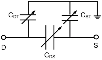
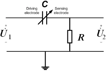
Figure 2.13: Equivalent circuit of the measurement circuit.
Figure 2.14: The Bode diagram of the measurement circuit described by Equation
(2.22)
Figure 2.15: System block diagram of capacitive imaging system. Figure 2.16: Block diagram of the lock-in amplifier.
Figure 2.17: Capacitive images of a Perspex plate with four flat bottomed holes. (a)
Amplitude plot and (b) phase difference plot.
Figure 2.18: Capacitive images of a steel plate with four flat bottomed holes. (a)
Amplitude plot and (b) phase difference plot.
Chapter 3
Figure 3.1: Evaluation of the penetration depth of a planar capacitive sensor,
where γ3% is the effective penetration depth[1].
Figure 3.2: Schematic diagram of the volume of influence (VOI) of the CI probe. Figure 3.3: Schematic diagrams for CI probes with different electrode separations.
(a) Separation d1, (b) Separation d2, (c)Cross-section of the probe with
d1 separation and (d) Cross-section of the probe with d2 separation.
Figure 3.4: Electrode array with each electrode numbered. Figure 3.5: Inducted voltages of different electrode pairs.
viii
array to a grounded steel rod.
Figure 3.7: Measured voltage with grounded rod moving away from array surface.
(a) Electrode pair 1-2 and (b) electrode pair 1-3.
Figure 3.8: Schematic diagrams for CI probes with and without guard electrodes.
(a) Top view of the CI probe without guard electrodes, (b) Top view of the CI probe with guard electrodes, (c) Cross-section of the CI probe without guard electrodes and (d) Cross-section of the CI probe with guard electrodes.
Figure 3.9: Experimental arrangement for electric field mapping.
Figure 3.10: Photograph of a CI probe with rectangular electrodes and guard
electrodes.
Figure 3.11: Experimentally measured electric field maps below the square
electrode pair shown in Figure 10, in a plane parallel to the electrodes and at a distance of 1 mm. Scans are shown for the guard electrode (a) electrically isolated and (b) grounded.
Figure 3.12: Diagram for triangular pair probe (a) back-ot- back (b) poin-to-point. Figure 3.13: Electric field plots along the dotted lines in each probe (a)
back-to-back triangular electrodes (b) point-to-point triangular electrodes.
Figure 3.14: Electric field plots along the dotted lines in each probe (a) with
grounded backplane (b) without backplane.
Figure 3.15: Photograph of concentric electrode design. The outer annular
electrode had inner and outer diameters of 32 mm and 48 mm respectively, and was separated from the inner disc electrode of 16 mm diameter by a thin grounded guard ring. An experimental scan was performed along the direction shown by the dotted line.
Figure 3.16: Field plots of electric field distributions from concentric electrodes
when (a) the outer annulus is excited, and (b) when the central disc is excited.
Figure 3.17: Decay of electric field amplitude as a measurement probe is scanned in
a perpendicular direction away from the PCB surface, starting from (a) the centre of the inner disc and (b) from within the outer electrode.
Figure 3.18: Diagram for concentric probes. (a) Without inner guard electrode and
(b) with an inner guard electrode.
ix
(right column).
Chapter 4
Figure 4.1: 2D Model geometry with elements.
Figure 4.2: The electric field distribution (equipotential lines) inside an insulating
specimen for (a) a uniform sample and (b) a sample containing an air-filled defect. The source electrode is on the right.
Figure 4.3: Schematic diagram for models to simulate corrosion under insulation
(CUI).
Figure 4.4: Simulations of the electric field distribution for a metal sample covered
with an insulator coating. Shown are results for (a) a uniform metal surface, (b) a metal surface containing a notch, and Non-dimensional models.
Figure 4.5: Schematic diagram for 2D non-dimensional models.
Figure 4.6: Schematic diagram for models with specimens of different thickness. Figure 4.7: Normalized capacitance against specimen thickness.
Figure 4.8: Schematic diagram for models with different lift-offs. Figure 4.9: Normalized capacitance against lift-off.
Figure 4.10: Normalized capacitance against permittivity for (a) a dielectric
specimen without grounded substrate and (b) a dielectric specimen with a grounded substrate.
Figure 4.11: Geometry of the probe and the specimen with a step.
Figure 4.12: Response for the conducting specimen with a step. (a) Electric
potential distribution for step of height 1.5B (b) change in capacitance.
Figure 4.13: Response for a dielectric specimen (step) (a) electric potential for step
of height 1.5B (b) change in capacitance.
Figure 4.14: Geometry of probe and specimen with a 7B groove.
Figure 4.15: Response for a conducting specimen (7B groove) (a) electric potential
for 7B groove (b) change in capacitance.
Figure 4.16: Response for a dielectric specimen (7B groove) (a) electric potential
for 7B groove (b) change in capacitance.
x
Figure 4.18: Response for a conducting specimen (3B groove) (a) electric potential
for 3B groove (b) change in capacitance.
Figure 4.19: Response for a dielectric specimen (3B groove) (a) electric potential
for 3B groove (b) Change in capacitance.
Figure 4.20: 3D model: (a) the computational domain (60 mm x 60 mm x 60 mm)
with a CI probe; (b) An example of FE meshing of the CI probe with the coordinate system used hereafter (axes have units of ‘cm’).
Figure 4.21: Plane coordinate systems for the 3 kinds of cross sections. Figure 4.22: Geometries of the probes.
Figure 4.23: Calculated electric field (presented in the form of electric potential) for
the (a) y=0 plane, (b) x=0 plane, (c) z=-0.2 plane, (d) z=-0.5 plane, (e) z=-1 plane, and (f) the planes that the plots were taken.
Figure 4.24: 3D model: A back-to-back triangular probe with a grounded steel
sphere.
Figure 4.25: Calculated electric field for the model with perturbation (presented in
the form of electric potential) for the (a) y=0 plane, (b) x=0 plane, (c) z=-0.2 plane, (d) z=-0.5 plane, (e) z=-1 plane, and (f) the planes that the plots were taken.
Figure 4.26: Model for evaluation the sensitivity distribution with 64 perturbations.
(a) 3D view and (b) 2D view with the coordinate system.
Figure 4.27: Sensitivity distribution in the z=-0.2 plane.
Figure 4.28: Schematic diagram for the model to obtain the sensitivity distribution. Figure 4.29: Distribution of positive, zero and negative sensitivity values.
Figure 4.30: Sensitivity distribution of Probe A. (a) x=0 plane, (b) y=0 plane, (c)
3D representation of y=0 plot and (d) 3D representation of the z=-0.2 plane plot.
Figure 4.31: Sensitivity distribution of Probe G. (a) x=0 plane, (b) y=0 plane, (c)
3D representation of y=0 plot and (d) 3D representation of the z=-0.2 plane plot.
Figure 4.32: Comparison between the sensitivity distributions of Probe C and Probe
xi
Figure 4.33: Comparison between the sensitivity distributions of Probe C and Probe
F (in the same colour scale). (a) and (b) the y=0 plane plots, (c) and (d) the z = -0.2 plane plots, (e) and (f) the z = -0.5 plane plots and (g) and (h) the z=-1.0 plane plots.
Figure 4.34: Comparison between the sensitivity distributions of Probe A and Probe
D (in the same colour scale). (a) and (b) the x = 0 plane plots, (c) and (d) the y = 0 plane plots, (e) and (f) the z = -0.2 plane plots, (g) and (h) the z = -0.5 plane plots and (i) and (j) the z = -1.0 plane plots.
Figure 4.35: Comparison among the sensitivity distributions of Probe A, Probe B
and Probe E (in the same colour scale). (a),(b) and (c) the y = 0 plane plots, (d),(e) and (f) the z = -0.2 plane plots, (g),(h) and (i) the z = -0.5 plane plots and (j),(k) and (l) the z = -1.0 plane plots.
Figure 4.36: Comparison of the sensitivity distributions of Probe A without and with
a dielectric sample. (a) and (b) the y = 0 plane plots, and (c) and (d) the z = -0.5 plane plots.
Figure 4.37: Comparison of the sensitivity distributions of Probe D without and with
a dielectric sample. (a) and (b) the y = 0 plane plots, and (c) and (d) the z=-0.5 plane plots.
Figure 4.38: Comparison of the sensitivity distributions of Probe A and Probe D for
(a) and (b) the plots of z = -0.5 plane with a dielectric specimen, and (c) and (d) the plots of z = -0.1 plane with a grounded conducting specimen.
Chapter 5
Figure 5.1: Electric field leakage.
Figure 5.2: PCB with metal enclosure and insulator protection. This layer was
typically made from polyester and was 0.1 mm thick.
Figure 5.3: (a) Uneven Surface and (b) lack of parallelism.
Figure 5.4: Schematic diagram of a 21mm thick Perspex plate containing flat
bottomed holes of depth (from left to right) 3 mm, 7 mm, 11 mm and 15 mm.
Figure 5.5: (a) Scan image from the surface containing the flat-bottomed holes. (b)
Scan image from the far (flat) surface. The depths of the holes are 15 mm, 11 mm, 7 mm and 3 mm from left to right.
Figure 5.6: Schematic diagram of a 9 mm thick aluminium plate containing flat
xii
mm.
Figure 5.7: Capacitive image of the aluminium plate containing flat bottomed
holes of depth (from left to right) 2 mm, 4 mm, 6 mm and 8 mm.
Figure 5.8: Schematic diagram of a 10mm thick steel plate containing flat
bottomed holes of depth (from left to right) 2 mm, 4 mm, 6 mm and 8 mm.
Figure 5.9: Capacitive image of the steel plate containing flat bottomed holes of
depth (from left to right) 2 mm, 4 mm, 6 mm and 8 mm.
Figure 5.10: Schematic diagram of a 5 mm laminated carbon fibre composite plate
containing two flat bottomed holes of depth 2 mm(left) and 4 mm(right).
Figure 5.11: Capacitive image of the laminated carbon fibre composite plate
containing two flat bottomed holes of depth 2 mm(left) and 4 mm(right).
Figure 5.12: Illustrations of the critical distance for (a) without specimen (in air)
and (b) with dielectric specimen.
Figure 5.13: Capacitive images of the Perspex plate, taken with the holes covered
by another Perspex plate with thickness (a) 2 mm, (b) 3 mm, (c) 4 mm and (d) 5 mm. The depths of the holes are 15 mm, 11 mm, 7 mm and 3 mm from top to bottom.
Figure 5.14: Capacitive images of the Perspex plate taken from the side with the
cone-type hole (a) without and (b) with the grounded substrate, and taken from the flat side(c) without and (d) with the grounded substrate.
Figure 5.15: Capacitive images of the Perspex plate containing four flat bottomed
holes, taken from the flat side (a) without and (b) with the grounded substrate. The depths of the holes are 15 mm, 11 mm, 7 mm and 3 mm from left to right.
Figure 5.16: Capacitive images of the steel plate containing flat bottomed circular
holes with the specimen (a) floating (b) connected to a second floating conductor and (c) grounded .The of depth of the holes are 2 mm, 4 mm, 6 mm and 8 mm from left to right.
Figure 5.17: Line plots of the 78th column of the capacitive images with the
xiii
Figure 5.18: Capacitive image of the steel plate containing flat bottomed circular
holes obtained by the point-to-point triangular probe with the specimen floating. The of depth of the holes are 2 mm, 4 mm, 6 mm and 8 mm from left to right.
Figure 5.19: Capacitive images of the Perspex plate, obtained from (a) the
back-to-back triangular CI probe (b) the point-to-point triangular CI probe and (c) the concentric CI probe. The depths of the holes are 15 mm, 11 mm, 7 mm and 3 mm from right to left.
Figure 5.20: Capacitive images of the aluminium plate, obtained from (a) the
back-to-back triangular CI probe (b) the point-to-point triangular CI probe and (c) the concentric CI probe. The depths of the holes are 2 mm, 4 mm, 6 mm and 8 mm from left to right.
Figure 5.21: Capacitive scan images obtained of the Perspex sample from
back-to-back triangular electrodes of size (a) 40 mm by 20 mm and (b) 20 mm by 10mm. The depths of the holes are 15 mm, 11 mm, 7 mm and 3 mm from left to right.
Figure 5.22: Capacitive images of the Perspex plate, taken at stand-off distances of
(a) 1 mm, (b) 3 mm, (c) 5 mm and (d) 7 mm. The scan was performed at the surface containing the flat-bottomed holes.
Figure 5.23: Capacitive images of the steel plate(grounded), taken at stand-off
distances of (a) 1 mm, (b) 3 mm, (c) 5 mm, (d) 7 mm, (e) 9 mm, (f) 11 mm, and (g) 13 mm. The scan was performed at the surface containing the flat-bottomed holes.
Figure 5.24: Capacitive images of the steel plate(floating), taken at stand-off
distances of (a) 1 mm, (b) 3 mm, (c) 5 mm, (d) 7 mm, (e) 9 mm, (f) 11 mm, and (g) 13 mm. The scan was performed at the surface containing the flat-bottomed holes.
Figure 5.25: Capacitive images of the aluminium plate containing flat bottomed
holes of depth (from left to right) 8 mm, 6 mm, 4 mm and 2 mm. (a) Image obtained for a 6 mm air gap between electrodes and the surface, and (b) result with a 5mm layer of insulating foam between the electrodes and the metal surface.
Figure 5.26: Schematic diagram of (a) a high density extruded polystyrene plate
with stepped thickness and (b) sample assembly and scan direction (cross-section view).
xiv
of the polystyrene plate (a) 10mm (b) 15mm (c) 20 mm and (d) 25 mm.
Figure 5.28: Capacitive scan images obtained of the Perspex sample with thin holes
from back-to-back triangular probe of size (a) 40 mm by 20 mm and (b) 20 mm by 10mm.
Figure 5.29: (a) The capacitive image of a hole (3 mm in diameter) on a Perspex
plate and (b) the calculated sensitivity distribution.
Figure 5.30: Capacitive images of a hole (3 mm in diameter) on an aluminium plate
with the plate (a) floating (b) connected to a second floating conductor and (c) grounded.
Figure 5.31: The capacitive image of a Perspex rod. (a) Intensity plot and (b)
contour plot.
Figure 5.32: Capacitive image of a Steel rod with the rod: (a) grounded and (b)
floating.
Figure 5.33: Capacitive images of the aluminium plate containing four narrow
cracks. (a) Intensity plot and (b) 3D plot.
Chapter 6
Figure 6.1: Photographs of the AIRBUS glass fibre sample. (a) Face A, (b) Face B. Figure 6.2: Two representations of the capacitive imaging scan of the Airbus glass
fibre sample. (a) Intensity plot and (b) contour plot.
Figure 6.3: Photographs of the pultruded glass-fibre reinforced polymer composite
with impact damage. (a) Face A and (b) Face B.
Figure 6.4: Two representations of the capacitive imaging scan of the glass fibre
sample with impact damage. (a) Intensity plot and (b) contour plot.
Figure 6.5: Photographs of the HEXCEL foam core sandwich structure. (a) Top
view-Face A, (b) side view, and (c) bottom view-Face B.
Figure 6.6: Schematic diagrams of the relative positions of the defects. (a) Top
view and (b) projection view from the cross section.
Figure 6.7: Two representations of the capacitive imaging scan of the form core
sandwich structure. (a) Intensity plot and (b) contour plot.
Figure 6.8: (a) Photograph of the aluminium honeycomb structure and (b)
xv
Figure 6.9: Two representations of the capacitive imaging of the aluminium
honeycomb structure. (a) Intensity plot and (b) contour plot.
Figure 6.10: Photograph of the aluminium honeycomb with folding failure covered
by glass fibre composite.
Figure 6.11: Two representations of the capacitive imaging scan of the simulated
sandwich structure with folding structure in the aluminium core. (a) Intensity plot and (b) contour plot.
Figure 6.12: Photograph of the aluminium honeycomb with some of the cells filled
with oil and water.
Figure 6.13: Two representations of the capacitive imaging scan of the simulated
sandwich structure with oil and water in the aluminium core. (a) Intensity plot and (b) contour plot.
Figure 6.14: Photograph of the AIRBUS panel.
Figure 6.15: Materials and lay up of the AIRBUS panel.
Figure 6.16: Schematic diagram of the distributions of defects in the AIRBUS panel. Figure 6.17: Two representations of the capacitive imaging scan of the AIRBUS
panel with defects. (a) Intensity plot and (b) contour plot.
Figure 6.18: Replot of the capacitive imaging scan along file C on the AIRBUS
panel in two representations. (a) Intensity plot and (b) contour plot.
Figure 6.19: Photographs of the carbon fibre composite with impact damage. (a)
Front face (Face A) with the impact and (b) reverse face (Face B).
Figure 6.20: Two representations of the capacitive imaging scan of the carbon fibre
composite with impact damage. (a) Intensity plot and (b) contour plot.
Figure 6.21: Amplitude plot of the carbon fibre composite with impact damage
obtained from air-coupled ultrasound scan.
Figure 6.22: (a) Photograph of the carbon fibre composite panel with superficial
burn damage and (b) the intensity plot of the capacitive image.
Figure 6.23: Photographs of the carbon fibre woven sample with the area to be
scanned highlighted.
Figure 6.24: Two representations of the capacitive imaging scan of the carbon fibre
xvi
Figure 6.25: (a) Photograph of a steel plate, immersed in brine for 10 days to cause
accelerated rusting in the lower section shown. (b) Capacitive image taken in air, highlighting the main areas of rusting, and (c) a similar image taken through a 5 mm thick insulating polymer foam coating.
Figure 6.26: Experiment setup for pipe inspection.
Figure 6.27: Comparison between the pipe cross-session profile (a) and CI result
(b).
Figure 6.28: Photographs of (a) the sandbox and (b) the metal objects (a steel ball
and a screw) to be buried.
Figure 6.29: Two representations of the capacitive imaging scan of the sandbox
with buried objects (a steel ball and a screw). (a) Intensity plot and (b) contour plot.
Figure 6.30: Photographs of (a) the sandbox and (b) the non-conducting object
(plastic pen cap) to be buried.
Figure 6.31: Two representations of the capacitive imaging scan of the sandbox
with buried objects (plastic pen cap). (a) Intensity plot and (b) contour plot.
Chapter 7
Figure 7.1: Model used for FE simulation of CI for concrete sample.
Figure 7.2: Simulations of the electric field distribution for a concrete sample.
Results are shown for (a) a uniform sample (b) a sample with a narrow crack on the surface, (c) a simulated void under the surface and (d) a steel rebar in the location shown.
Figure 7.3: Concrete specimen with a crack on the surface. (a) Photograph of top
surface containing the crack, and (b) schematic diagram of the crack geometry.
Figure 7.4: Capacitive imaging results for concrete sample with a crack on the
surface.
Figure 7.5: (a) Photograph and (b) schematic diagram of a concrete sample with a
hidden channel of two different depths (30 mm and 60 mm).
Figure 7.6: Capacitive imaging results for concrete sample with a hidden stepped
xvii
Figure 7.7: Concrete sample with a single rebar of 10 mm diameter placed
symmetrically within the thickness of a 30 mm thick concrete sample. (a) Photograph of sample, and (b) schematic diagram.
Figure 7.8: Capacitive imaging results for the concrete sample of Figure 9,
containing a single rebar. (a) Grounded rebar and (b) electrically-floating rebar.
Figure 7.9: Concrete sample with rebars (a) Photograph of sample, and (b)
schematic diagram.
Figure 7.10: Capacitive imaging results for the concrete sample shown in Figure
7.9.
Chapter 8
Figure 8.1: Photograph of the CI probe comprises two pins as active electrodes. Figure 8.2: (a) Photograph of a two pence coin and (b) the capacitive imge of the
coin shown in gray scale.
Figure 8.3: (a) Photograph of the coils and (b) the cross-sectional view. Figure 8.4: Equivalent circuit of the eddy current mode.
Figure 8.5: Results of the flat bottomed hole on a steel plate obtained from the
eddy current mode.(a)The intensity plot and (b)the contour plot.
Figure 8.6: Schematic diagram of the system using coils in the capacitive image
mode.
Figure 8.7: Results of the flat bottomed hole on a steel plate obtained from the
capacitive imaging mode.(a)The intensity plot and (b) the contour plot.
Figure 8.8: Line plots from images obtained from (a) the capacitive imaging mode
and (b )the eddy current mode
Figure 8.9: Combinting the images obtained from the eddy current mode and the
capacitive imaging mode.(a)The intensity plot and (b)the contour plot.
Figure 8.10: Line plot from the combined image.
Figure 8.11: Results of the flat bottomed hole on a Perspex plate obtained from the
capacitive imaging mode.(a) The intensity plot and (b) the contour plot.
Figure 8.12: Photograph of modified concentric electrode design. The outer annular
xviii
respectively, and the inner disc electrode (before the hole was drilled) was 16 mm in diameter.
Figure 8.13: Schematic diagram of the system using the modified concentric CI
probe.
Figure 8.14: Results for (a) the Perspex plate and (b) the aluminium plate.
Figure 8.15: Capacitive images of the Perspex plate, taken at lift-off distances of (a)
1 mm, (b) 3 mm, (c) 5 mm and (d) 7 mm. The scan was performed at the surface containing the flat-bottomed holes.
Figure 8.16: Capacitive images of the aluminium plate (grounded), taken at
xix
List of Tables
Chapter 2
Table 2-1: Capacitances for some typical capacitors. Chapter 3
Table 3-1: Measured induced voltage for selected electrode pairs. Chapter 4
Table 4-1: Specifications of probes shown in Figure 4.22. Chapter 7
xx
Acknowledgements
First of all, I am infinitely grateful to my supervisor, Professor David Hutchins, who has endlessly supported me in the development and writing of this thesis with his patience, excellent supervision and seemingly limitless knowledge. He also significantly contributed to all my publications that originated at Warwick and supplied the much needed encouragement and optimism at the tough times. One simply could not wish for a better supervisor. I also greatly appreciate his financial support throughout my Ph.D. course. I would also like to thank Dr. Duncan Billson for his caring discussions and advice on this research.
I would like to thank Dr. Geoff Diamond for his timely advice, discussions and novel ideas at the early stage of this research. My thanks also go to Dr. Lee Davis for his assistance with computers, printers, experimental setups, and numerous devices, apparatus that had to be brought to life over the years in the lab. I would like to express my thanks to the team of technicians of the School of Engineering, especially Mr. Huw Edwards, Mr. Frank Courtney, Mr. Ian Griffith and Mr. Colin Banks, for manufacturing some of the components or specimens used during this research. I would also like to thank former members of the AIM Lab and my fellow PhD students: Dr. Chuan Li, Dr. Eddie Ho, Dr. Prakash Pallav, Mrs. Celine Canal, Mr. Aamer Saleem and Mr. Vipin Seetohul for their companionship and cooperation.
xxi
Declaration
The work described in this thesis was conducted by the author, except where stated otherwise, in the School of Engineering, University of Warwick between the dates of March 2007 and February 2011. No part of this work has been previously submitted to the University of Warwick or any other academic institution for admission to a higher degree. All publications to date arising from this thesis are listed after the bibliography.
xxii
Summary
This thesis describes the development and characterization of a novel NDE method-the Capacitive Imaging (CI) technique. The CI technique employs a pair of (or multiple) electrodes to form a co-planar capacitor, and uses the fringing quasi-static electric field established across the electrodes to investigate specimens of interest. In general, the CI probe is sensitive to surface and hidden defects in insulating materials, and surface features on conducting materials. The CI technique is advantageous for its non-contact and non-invasive nature, and the capacitive coupling allows the CI technique to work on a wide variety of material properties.
The theoretical background to the CI technique has been developed. It is shown that in the frequency range of operation (10 kHz to 1 MHz), the quasi-static approximation is valid and the Maxwell’s Equations describing the general electromagnetic phenomena can be simplified. The practical implementation of the CI system is based on this analysis, and it is shown that the CI technique has features that can complement techniques such as eddy current methods that are already established in NDE.
The design principles of the CI probes that are required for an optimum imaging performance have been determined, by considering the key measures of the performance including the depth of penetration, the measurement sensitivity, the imaging resolution and the signal to noise ratio (SNR). It has been shown that the operation frequency is not an influential factor - the performance of the CI probe is determined primarily by the geometry of the probe (e.g. size/shape of the electrodes, separation between electrodes, guard electrodes etc.). Symmetric CI probes with triangular-shaped electrodes were identified as a good general purpose design. Finite Element (FE) models were constructed both in 2D and 3D in COMSOLTM to predict the electric field distributions from CI probes. Effects of thickness of specimen, lift-off distance and relative permittivity value etc were examined using the 2D models. The sensitivity distributions of different CI probes were obtained from the 3D models and were used to characterize the imaging ability of the given CI probes.
1
Chapter 1
Introduction
1.1 Introduction
destructive Evaluation (NDE), which is also sometimes referred to as Non-destructive testing (NDT) or Non-Non-destructive Inspection (NDI), has been defined as comprising those test methods used to evaluate the properties of a material, component or system without causing damage. NDE techniques has found numerous industrial applications such as the inspection of pipelines, rails, pressure tanks, aircraft, bridges and many other components, where the risks are high and precautions are required. The main functions of NDE are [1]:
• To ensure the system freedom from defects likely to cause failure.
• To ascertain the dimensions of a component or structure.
• To determine the physical and structural properties of materials of interest.
NDE techniques have developed rapidly in recent years. A variety of physical principles are used, and there is no single method around which a “black box” may be built to satisfy all requirements in all circumstances. Some examples include dye penetrant testing, ultrasonic testing, and acoustic emission. Electromagnetic techniques cover almost all the frequency spectrum, starting from DC (potential drop methods and magnetic leakage detection), through the radio frequency (RF) region (eddy current) and microwave region (ground penetrating radar), also covering the THz (THz or millimetre-wave imaging) and the infrared region (IR imaging and
themorgraphy). Ionizng techniques occur at even higher frequencies (X-ray and γ-ray
radiography). This thesis is primarily concerned with the radio frequency region, as the capacitive imaging (CI) technique to be discussed mainly operates at frequencies of up to 1 MHz.
capacitive sensors. The final section gives the objectives of the research and an overview of the remaining chapters of this thesis.
1.2 Electrical and magnetic methods of NDE
The physical and structural properties of a specimen can be related to the electrical and magnetic properties (including electrical conductivity, electrical permittivity and magnetic permeability) of the material. By assessing the electrical and magnetic property variations, defects within the specimen can be detected. In this section, a brief review of these electrical and magnetic methods is presented.
1.2.1 Eddy current methods
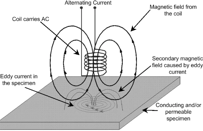
The eddy current method works on the principles of electromagnetic induction and can be applied to electrically conducting and/or magnetically permeable materials. In the eddy current technique, a current carrying coil (typically sinusoidal AC) is used to excite a time varying magnetic field in the material under test. The time varying magnetic field will induce conduction currents (if the material is conducting) and magnetization currents (if the material is permeable) in the specimen. According to Lenz’s Law, both kinds of currents can generate a secondary magnetic field in the opposite direction and contribute to the total magnetic field, as shown in Figure 1.1.
Figure 1.1: The induction of eddy current.
[image:26.595.155.485.496.708.2]The total magnetic field, which contains the effects of the specimen, is then sensed by either the excitation coil or a separate sensing coil. If there is a defect, the coil impedance will be changed, which can be measured and correlated with the defect. As a vector quantity, the impedance change has both amplitude and phase angle. The amplitude provides information about the severity of the defect (e.g. the size). For the phase angle, as the generation of eddy currents can be considered as a time dependent process, meaning that the eddy currents below the surface take a little longer to form than those at the surface. This provides information about the defect location or depth if comparison is made to a known reference (lift-off).
The density of the eddy current is non-uniform and decays through the thickness of the specimen, due to the skin effect. To characterize the penetration depth, the term “standard depth of penetration” is defined as the depth at which the eddy current density is 37% of its value at the surface and commonly used in eddy current
inspections. The standard depth of penetration δ can be calculated from the following
equation:
1
f δ
π μσ
= , (1.1)
where f is the excitation frequency of the current, μis the magnetic permeability
and σ is the electrical conductivity. It can be seen from Equation (1.1) that for a given
material the depth of penetration is inversely proportional to the square root of the frequency. Therefore, high frequencies can be to used to detect very shallow defects (cracks, flaws) in a material, and low frequencies can be used to detect sub-surface buried defects and to test highly conductive materials [2].
In the past few decades, the basic eddy current sensors have evolved into many more sophisticated types, such as sensors with planar coils [3], sensors using giant magnetoresistive (GMR) magnetometers to detect the secondary magnetic field [4], and sensors using pulsed excitation [5].
Although widely used in various NDE applications, the limitations of the eddy current methods have been recognized [6]. A few key limitations are:
• It works only on conducting materials.
• Penetration thickness for complete volumetric eddy-current inspection is
limited.
• Inspection of ferromagnetic materials is difficult if the saturation method is not
applicable.
• Operator skill is necessary for meaningful testing and evaluation.
1.2.2 Potential drop methods
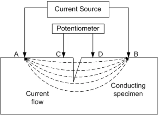
The basic principle for the potential drop method is the use a pair of electrodes to inject a steady current through a conducting specimen, and another pair to measure the resultant potential difference across a small distance (a few millimeters) [7]. There are two basic types of potential drop methods, namely the DC potential drop (DCPD) and AC potential drop (ACPD). Figure 1.2 shows the arrangement for both the DCPD and the ACPD measurements. Four electrodes (A, B, C and D) are in contact with the
conducting specimen. A current I (DC or AC) is passed through the specimen
between electrode A and B, the potential difference between electrodes C and D, V, is measured.
Figure 1.2: Arrangement for potential drop measurements.
[image:28.595.183.461.477.681.2]The ratio V/I contains information on the specimen and can be used to determine wall thickness or size and position of cracks [8]. The DCPD methods are usually used to measure depth of surface breaking cracks after they have been detected by other techniques, by comparing the measured potentials from both a normal area and the area surrounding the crack. For ACDP methods, unlike the DCPD where a large uniform direct current is throughout the whole volume of the material, the alternating current can only be carried near the conducting surface due to the “skin effect”.
In both DCPD and ACPD methods, intimate contact is needed between the electrodes and the specimen to establish good electrical contact, and sometimes the current will heat the specimen and cause safety problems.
1.2.3 Magnetic methods
For magnetic methods, a magnetic field is applied to the specimen under test and the resultant changes of magnetic flux associated with defects in the targeting region are observed. A review of the magnetic methods can be found in [9, 10]. Figure 1.3 shows how discontinuities of magnetic permeability (e.g. a surface slot) affect the lines of induced magnetic flux.
Figure 1.3: Magnetic flux leakage at a slot cut into a magnetized specimen.
It can be seen from Figure 1.3 that there is magnetic flux leakage normal to the surface due to the presence of the slot. North and south magnetic poles will appear on the opposite sides of the slot [1]. Flux leakage also takes place at the opposite surface with a lower density, but over a wider region.
6
The magnetic field in the specimen can be generated by placing a magnetized yoke in contact with the specimen, passing a current through the specimen, or using magnetic induction using a coil or a threading bar. The flux leakage associated with possible defects can then be detected by magnetic particles, magnetic tape (magnetography) or sensing coils and other sensors (e.g. Hall sensors, magnetoresistive sensors or the superconducting quantum interface device (SQUID). Magnetic methods are confined to ferromagnetic materials and sometimes contact with specimen is required (e.g. metal clamps for the current injection).
1.2.4 Capacitive methods
Traditional capacitive methods rely on the capacitive coupling between the active electrode pairs, and utilize the electric field as the probing field to interrogate specimens. Capacitive techniques have not been widely used for NDE, in contrast to say eddy current methods. This is partially due to the historic use of conducting materials (which are suitable for eddy current inspections) in critical components. Secondly, for some capacitive methods, the specimen is often sandwiched between two electrodes so that the specimen is exposed to a uniform electric field, which is only practical for specimens in a relatively thin plate shape and requires access to both sides of the specimen. However, in recent years with the ever increasing use of non-conducting materials (i.e. polymers and glass fibre composites) in manufacturing and the development of co-planar capacitive sensors, the number of NDE applications for which the capacitive methods may be appropriate has been expanding.
thermal conductivity [20], etc. In most of the cases, such a measurement is taken by an LCR meter or a basic impedance measurement circuit with a single frequency excitation, and the measured capacitance is then correlated to the measured property via models [21] or databases [22] generated prior to the measurement. However sometimes, the measurement is taken over a range of frequencies and the frequency dependent effective permittivity can be determined via an impedance analysis. Inter-digital fringing field sensors (see Figure 1.4) are the most commonly-seen design, because of the increased output capacitance between the electrodes due to the spatially periodic structure [23] [24].
Figure 1.4: Diagram of a three-wavelength interdigital sensor with spatial
periodicities of 2.5 mm, 5.0 mm, and 1.0 mm [25] ( the term wavelength refers to the spatial periodicity of the interdigital structure that equals to the distance between
neighbouring fingers of the same electrode).
Other types of capacitive sensor have been used for the detection of inhomogeneities. For example, capacitive array sensors with differential output have been used to precisely define the edges of surface and subsurface slots in dielectrics and surface slots in conductors [21], rectangular capacitive sensors are used for the detection of water intrusion [26] and voids [27] in composite structures, and concentric capacitive sensors are used for the detection of a localized anomaly in a multi-layered structure, such as an aircraft radome [28]. In addition, capacitive sensor arrays with multi
[image:31.595.201.441.270.514.2]sensing electrodes (shown in Figure 1.5) have also been used to image buried objects, such as landmines and unexploded ordnance (UXO) [29].
Figure 1.5: Capacitive sensor with single driving and multi sensing electrodes [29].
In this thesis, the above methods are extended by using capacitive techniques for a wide-ranging investigation into possible NDE applications.
1.2.5 Other electromagnetic methods
There are also techniques that operate in the RF region but do not fall into any of the categories mentioned in Section 1.2.1 to Section 1.2.4.
The first one is called the electric potential (displacement current) sensor (EPS) [30], which can be used for the inspection of conducting specimens. These sensors have
ultra-high input impedance (1017Ω) and can detect small electric potentials with high
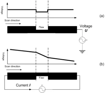
sensitivity. Basically, by scanning the EPS over the surface of a specimen, the electric potential map of the scanned plane (in the vicinity of the surface) can be obtained. EPS was initially designed for the non-invasive detection of the weak electrical signals generated by the human body, for example, the electrocardiogram (ECG) and the electroencephalogram (EEG), and the feasibility for NDE has been demonstrated by the inspection of carbon fibre composite [30] and stainless steel [31]. The EPS approach can be used in both voltage and current mode. In the voltage mode, the conducting specimen is connected to an AC voltage via an electrode attached to the specimen. This creates an equipotential surface on the sample. If there is any flaw on
the surface, there will be a drop of the measured potential in the plane parallel to the surface of the specimen, as shown in Figure 1.6(a). The voltage mode only works for surface features, as the equipotential surface blankets everything underneath it. For hidden flaws, the current mode is need. In the current mode, a finite current is injected through the specimen by two electrodes at both ends of the specimen. This creates a voltage gradient along the length of the sample which should be uniform in the absence of defects. If a flaw exists in the path of the current (on the surface or within the skin depth), it will be reflected as local changes in conductivity (resistivity) and will be made manifest through the surface electric potential map above the sample (e.g. registered (locally) as relatively steep gradients, as shown in Figure 1.6(b)).
Figure 1.6: Schematic diagram for EPS in (a) voltage mode and (b) current mode.
The second technique is called capacitive resistivity (CR) technique [32], which is a geographical technique for the non-intrusive characterization of the shallow subsurface of the earth’s surface. Fundamentally, the CR technique has evolved from the DC resistivity (potential drop) method (shown in Figure 1.7(a)) by changing the resistive coupling (direct contact between the electrodes and ground) into capacitive
[image:33.595.153.496.305.605.2]coupling (non-contact), as shown in Figure 1.7(b). In a similar way to the DC resistivity method, the measurement circuit of the CR technique can be divided into two parts: a transmitter circuit used to energise the ground, and a receiver part to measure a potential. In practice, the sensors are usually in the form of “line-antenna” or “plate-wire combination”. Recently, the CR sensor with an inductive source has also been reported [33].
Figure 1.7: Schematic diagram for (a) the DC resistivity method and (b) the
capacitive resistivity method[32].
1.3 A general review on capacitive sensors
In addition to the above, many other different kinds of capacitive sensors have been designed, which are all based on the same physical phenomenon. A review of these capacitive sensors will help to understand the CI technique presented in this thesis.
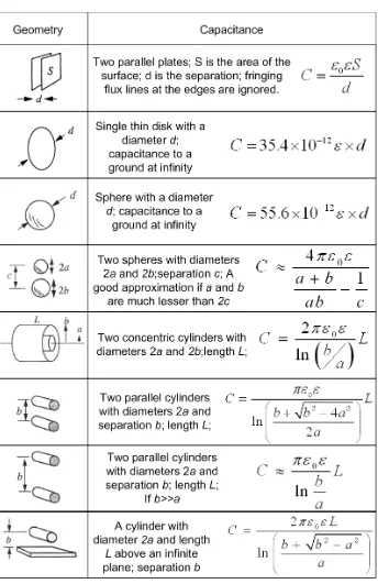
The first reference to capacitive sensors is found in Nature,1907 [34], and the capacitive sensors have been developing since then. Fundamentally, most of the capacitive sensors are based on extremely simple physical concepts-the simple parallel capacitor model [35]. In this model, the capacitance, C, is related to other parameters by a simple relationship:
/
C=εA d , (1.2)
11
where d is the plate separation, A is the plate area and ε is the dielectric constant of the
material sandwiched between the plates. Nowadays, capacitive sensors have a wide variety of uses. Typical applications of capacitive sensors can be loosely placed into the following categories:
Proximity sensing- Capacitive proximity sensors sense distances to nearby targets without requiring contact. There are basically two types. In the first, the sensor itself forms one plate and the object to be measured forms the other. For theses sensors, the target object has to be conducting. The second type uses the principle of fringing capacitance, and the target object could either be a conductor or an insulator. The application of proximity sensors includes personnel protection (alarm will be triggered if the operator’s hand is too close to the machine) [36, 37], light switches (light will be switched on for an approaching person) and vehicle detection.
Measurement - Capacitive coupling between electrodes can be used to measure
physical quantities such as displacement [38], thickness [39], rotation [40], movement [41], pressure [42], humidity [43], properties of substance [44], etc. The measured
physical quantity can change one (or some) of the three parameters (ε, A and d)
mentioned in Equation (1.2) and hence a measurable capacitance change. For example, in a capacitive humidity sensor, it is the change in the dielectric constant of the
material (humidity in air), ε, that changes the capacitance. There are many examples
in the literature [45-47], e.g. for multi-interface detection between air/liquid.
Fingerprinting - Capacitive sensor arrays with extremely small (~ 0.05 mm) sensing pair are used to acquire tiny surface features (such as ridges and valleys on human skin), and prototypes of fingerprint acquisition systems [48, 49] have been reported in the literature.
Flow Tomography - Electrical Capacitance Tomography (ECT) offers a method for measuring the physical properties of solids, liquids and gasses [32]. ECT systems usually operate under the 2D assumption and image the material properties across the cross-section area (e.g. a section of pipeline). The cross-section to be imaged (say of flow in a pipe) is surrounded by a set of capacitive electrodes which are mounted inside (conducting walls) or outside (insulating walls) of the vessels, as shown in Figure 1.8. The changes in capacitance between all possible combinations of electrode pair (for a 12 electrodes system, as shown in Figure 1.8, the number is 66) which occur when material with different electrical properties is introduced to the imaging cross-section are measured. The image of the cross-section is then reconstructed with these measured capacitances via various reconstruction algorithms. It is an excellent method for analyzing multi-phase flow in oil and gas pipelines.
Figure 1.8: (a) Cross-sectional view and (b) 3D schematic diagram of a typical ECT
sensor with 12 electrodes[53].
1.4 Objectives of the research and outline of the thesis
The thesis describes the work conducted on the development and characterisation of the capacitive imaging (CI) technique, which has the potential to overcome some of the problems that may be encountered by other electrical and magnetic NDE approaches. Although the idea of using the capacitive coupling between active electrodes to measure physical quantities has existed for some time, the imaging ability of capacitive sensors for NDE purposes has yet to be studied in any great detail. As a general aim, this thesis seeks to investigate this aspect by presenting a full
13
appraisal of all aspects of the proposed CI technique. The scope of the research and the main objectives are:
• To investigate the fundamental concepts of CI, and to provide a unified
description of the physical principles that dictate its practical implementation.
• To study the design principles of CI probes, and provide recommendations for
probe design and selection.
• To characterize fabricated CI probes and evaluate their imaging ability.
• To identify influential system parameters, and to study the effects of variations
in these parameters on the results obtained in an NDE measurement.
• To prove the practical validity of the CI technique by experimentation, and to
evaluate the use of CI in a range of different applications.
These objectives are reflected in the following thesis structure:
Chapter 2 gives a detailed introduction of the proposed CI technique, beginning with a description of the CI concept and fundamentals. This is followed with a brief review of the theoretical background, including the Maxwell equations, the quasi-static approximation, the electrical properties of the specimens under test and the calculation of capacitance. The modes of operation are then classified depending on the electrical conditions of the specimens along with the corresponding equivalent circuits. The instrumentation of the CI system is subsequently presented followed with some preliminary results - images formed by amplitude variation and phase difference from scans conducted on Perspex and steel plate. Finally, the proposed CI technique is compared with the widely used eddy current technique and conventional capacitive sensors.
14
geometries. Design factors, such as separation between electrodes, guard electrodes, and electrode shapes are also discussed and examined experimentally.
In Chapter 4, Finite Element (FE) models are constructed in COMSOLTM and used to
model the CI technique. Firstly, the 2D models are used to demonstrate how the electric fields from a CI probe interact with different specimens. Effects of specimen thickness, lift-off distance and relative permittivity values on the CI probe response are carried out, together with simulations of flaw detection. Subsequently, 3D models were constructed, to provide a more accurate prediction of the probe performance. The measurement sensitivity of CI is then studied based on the 3D models. Firstly, the perturbation method is used and a rather coarse sensitivity map is obtained from the 3D model. A detailed derivation of the sensitivity distribution function is then presented, based on which a more refined sensitivity map can be obtained. Finally, the sensitivity maps of probes with different geometries are obtained and compared, providing an overview of the CI probe performance and an assessment for the influences of the sensor design parameters.
In Chapter 5, a series of basic experiments to validate the concept of the CI technique is described. The results of these experiments are used to verify the predictions of the probe performances discussed in Chapters 3 and 4. Firstly, some instrumentation- related issues are considered. Secondly, typical results including the detection of surface and hidden defects in non-conducting specimens, and surface features on conducting specimens, are presented. Thirdly, practical CI measurements are undertaken with various samples under different situations and using different probes, through which the defect detection ability of the CI technique is assessed. Subsequently, surface features on metals are successfully detected through a relatively thick insulation layer, indicating a possible application for the detection of the Corrosion under Insulation (CUI). Finally, the responses of the CI probes to features smaller in size comparing to the probe sensing area are examined.
15
preliminary experiments to image buried objects (both conducting and non-conducting) using the CI technique is also presented.
Chapter 7 examines how the CI technique can be used on the inspection of concrete specimens. The introductory part of this chapter provides a brief review of the commonly used methods for concrete inspection. 2D FE models are then used to predict how the electric field interacts with concrete structures. The results of experiments conducted on different concrete specimens are also presented, including samples with surface cracks, hidden air voids and rebars. Finally, the limitations encountered in the concrete inspection using the CI technique are discussed.
In Chapter 8, modified CI probes, including probes using two pins or two coils as active electrodes and using a high impedance oscilloscope probe as sensing electrode, are proposed and investigated. It is shown that this extends the range of applications of CI methods.
16
1.5 References
[1] J. Blitz, "Electrical and Magnetic Methods og Non-destructive Testing
(Second Edition)," Chapman and Hall, 1997, p. 44.
[2] H. Yamada, T. Hasegawa, Y. Ishihara, T. Kiwa, and K. Tsukada, "Difference
in the detection limits of flaws in the depths of multi-layered and continuous aluminum plates using low-frequency eddy current testing," NDT & E International, vol. 41, pp. 108-111, 2008.
[3] R. J. Ditchburn and S. K. Burke, "Planar rectangular spiral coils in
eddy-current non-destructive inspection," NDT & E International, vol. 38, pp. 690-700, 2005.
[4] J.-T. Jeng, G.-S. Lee, W.-C. Liao, and C.-L. Shu, "Depth-resolved
eddy-current detection with GMR magnetometer," Journal of Magnetism and Magnetic Materials, vol. 304, pp. e470-e473, 2006.
[5] G. Y. Tian and A. Sophian, "Reduction of lift-off effects for pulsed eddy
current NDT," NDT & E International, vol. 38, pp. 319-324, 2005.
[6] G. Van Drunen and V. S. Cecco, "Recognizing limitations in eddy-current
testing," NDT International, vol. 17, pp. 9-17, 1984.
[7] R. Ghajar, "An alternative method for crack interaction in NDE of multiple
cracks by means of potential drop technique," NDT & E International, vol. 37, pp. 539-544, 2004.
[8] H. Sun, "Electromagnetic methods for measuring material properties of
cylindrical rods and array probes for rapid flaw inspection," PhD Thesis, Iowa State University, 2005.
[9] D. C. Jiles, "Review of magnetic methods for nondestructive evaluation:
17
[10] D. C. Jiles, "Review of magnetic methods for nondestructive evaluation (Part 2)," NDT International, vol. 23, pp. 83-92, 1990.
[11] A. V. Mamishev, "Interdigital dielectrometry sensor design and parameter estimation algorithms for non-destructive materials evaluation," in Electrical Engineering and Computer Science Cambridge: PhD thesis, Massachusetts Institute of Technology, 1999.
[12] E. Bozzi and M. Bramanti, "A planar applicator for measuring surface dielectric constant of materials," Instrumentation and Measurement, IEEE Transactions on, vol. 49, pp. 773-775, 2000.
[13] P. A. von Guggenberg and M. C. Zaretsky, "Estimation of one-dimensional complex-permittivity profiles: a feasibility study," Journal of Electrostatics, vol. 34, pp. 263-277, 1995.
[14] A. V. Mamishev, A. R. Takahashi, Y. Du, B. C. Lesieutre, and M. Zahn, "Parameter estimation in dielectrometry measurements," Journal of Electrostatics, vol. 56, pp. 465-492, 2002.
[15] D. S. Schlicker, Yanko; Washabaugh, Andrew and Goldfine, Neil "Capacitive Sensing Dielectrometers for Noncontact Characterization of Adhesives and Epoxies," in Society Plastics Engineers (SPE) ANTEC, 2002.
[16] K. G. Bang, J. W. Kwon, D. G. Lee, and J. W. Lee, "Measurement of the degree of cure of glass fiber-epoxy composites using dielectrometry," Journal of Materials Processing Technology, vol. 113, pp. 209-214, 2001.
[17] X. Li, A.S.Zyuzin, and A. V. Mamishev, "Measuring moisture content in cookies using dielectric spectroscopy," Electrical Insulation and Dielectric Phenomena, 2003. Annual Report. Conference on , vol., no., pp. 459- 462, 19-22 Oct. 2003
18
[19] M. C. Zaretsky, P. Li, and J. R. Melcher, "Estimation of thickness, complex bulk permittivity and surface conductivity using interdigital dielectrometry," Electrical Insulation, IEEE Transactions on, vol. 24, pp. 1159-1166, 1989.
[20] J. T. L. Neil J. Goldfine, Yanko Sheiretov, Paul J. Zombo, "Dielecirometers and magnetometers, suitable for in-situ inspection of Ceramic and Matellic Coated Components," SPIE proc, vol. 2459, pp. 164-174, 1995.
[21] M. Gimple and B. A. Auld, "Variable geometry capacitive probes for multipurpose sensing," Research in Nondestructive Evaluation, vol. 1, pp. 111-132, 1989.
[22] D. E. Schlicker, "Imaging of absolute electrical properties using electroquasistatic and magnetoquasistatic sensor arrays," PhD thesis, Massachusetts Institute of Technology 2005.
[23] Y. Sheiretov and M. Zahn, "Modeling of spatially periodic dielectric sensors in the presence of a top ground plane bounding the test dielectric," Dielectrics and Electrical Insulation, IEEE Transactions on, vol. 12, pp. 993-1004, 2005.
[24] A. V. Mamishev, K. Sundara-Rajan, Y. Fumin, D. Yanqing, and M. Zahn, "Interdigital sensors and transducers," Proceedings of the IEEE, vol. 92, pp. 808-845, 2004.
[25] A. V. Mamishev, S. R. Cantrell, Y. Du, B. C. Lesieutre, and M. Zahn, "Uncertainty in multiple penetration depth fringing electric field sensor measurements," Instrumentation and Measurement, IEEE Transactions on, vol. 51, pp. 1192-1199, 2002.
[26] A. A. Nassr, W. H. Ahmed, and W. W. El-Dakhakhni, "Coplanar capacitance sensors for detecting water intrusion in composite structures," Measurement Science and Technology, vol. 19, p. 075702, 2008.
19
[28] T. Chen and N. Bowler, "Analysis of a concentric coplanar capacitive sensor for nondestructive evaluation of multi-layered dielectric structures," Dielectrics and Electrical Insulation, IEEE Transactions on, vol. 17, pp. 1307-1318, 2010.
[29] D. Schlicker, A. Washabaugh, I. Shay, and N. Goldfine, "Inductive and capacitive array imaging of buried objects," Bindt Insight, vol. 48, pp. 02-306, 2006.
[30] W. Gebrial, R. J. Prance, C. J. Harland, P. B. Stiffell, H. Prance, and T. D. Clark, "Non-contact imaging of carbon composite structures using electric potential (displacement current) sensors," Measurement Science and Technology, vol. 17, pp. 1470-1476, 2006.
[31] R. Prance, W. Gebrial, and C. Antrobus, "Depth profiling of defects in stainless steel using electric potential sensors and a non-contact AC potential drop method," Insight, vol. 50, pp. 95-97, 2008.
[32] O. Kuras, "The capacitive resistivity technique for electrical imaging of the shallow subsurface," PhD thesis, The university of Nottingham, 2002.
[33] C. H. Adams, "Capacitive Array Resistivity with an Inductive Source," in School of Applied Science: PhD thesis, RMIT University, 2008.
[34] L. K. Baxter, Capacitive Sensors: Design and Applications: Wiley-IEEE Press, 1996.
[35] A. Stuart and J. A. Allocca, "Transducers: Theory and Applications," Reston Publishing, 1984, p. 89.
[36] P. Malcovati, A. Baschirotto, A. d'Amico, C. Natale, M. Norgia, and C. Svelto, "Capacitive Proximity Sensor for Chainsaw Safety," in Sensors and Microsystems. vol. 54: Springer Netherlands, 2010, pp. 433-436.
20
[38] F. Zhu, J. W. Spronck, and W. C. Heerens, "A simple capacitive displacement sensor," Sensors and Actuators A: Physical, vol. 26, pp. 265-269, 1991.
[39] H. Carr and C. Wykes, "Diagnostic measurements in capacitive transducers," Ultrasonics, vol. 31, pp. 13-20, 1993.
[40] Y. Xu, T. Zhang, H. Wang, and D. Chen, "Smart floating element flowmeter based on a capacitive angular displacement transducer," Flow Measurement and Instrumentation, vol. 16, pp. 1-6, 2005.
[41] J. C. Lotters, W. Olthuis, P. H. Veltink, and P. Bergveld, "Design, realization and characterization of a symmetrical triaxial capacitive accelerometer for medical applications," Sensors and Actuators A: Physical, vol. 61, pp. 303-308, 1997.
[42] W. H. Ko and Q. Wang, "Touch mode capacitive pressure sensors," Sensors and Actuators A: Physical, vol. 75, pp. 242-251, 1999.
[43] Y. Kim, B. Jung, H. Lee, H. Kim, K. Lee, and H. Park, "Capacitive humidity sensor design based on anodic aluminum oxide," Sensors and Actuators B: Chemical, vol. 141, pp. 441-446, 2009.
[44] N. Kirchner, D. Hordern, D. Liu, and G. Dissanayake, "Capacitive sensor for object ranging and material type identification," Sensors and Actuators A: Physical, vol. 148, pp. 96-104, 2008.
[45] H. Caniere and et al., "Horizontal two-phase flow characterization for small diameter tubes with a capacitance sensor," Measurement Science and Technology, vol. 18, p. 2898, 2007.
![Figure 1.4: Diagram of a three-wavelength interdigital sensor with spatial periodicities of 2.5 mm, 5.0 mm, and 1.0 mm [25] ( the term wavelength refers to the spatial periodicity of the interdigital structure that equals to the distance between neighbouri](https://thumb-us.123doks.com/thumbv2/123dok_us/9686181.470033/31.595.201.441.270.514/wavelength-interdigital-periodicities-wavelength-periodicity-interdigital-structure-neighbouri.webp)