Operation and Maintenance
Manual
Data Streamer™
Emulates IBM 8809
FCC CERTIFIED COMPUTER EQUIPMENT
This equipment, freestanding with shielded Data and Control Cables,
complies with Part
15,
Subpart
J
of FCC Rules Governing Class
A
Computing Devices Operated In
A
Commercial Environment. However,
the equipment generates radio frequency energy and, when operated in
a residential area, the user must take adequate precautions against
interference to radio communications.
Copywrite
01987 by Kennedy Company
All
rights reserved.
No part of this work covered by the copyright
106-6809-001B
SECTION I
APPLICATION DATA
1.1
INTRODUCTIONThe Model 6809 is a low cost, streaming tape drive whose main application is as a backup to disk drives. The 6809 has two data transfer modes - the streaming mode and the start/stop mode. In the streaming mode the drive moves tape at 100 inches per second, transferring data at the rate of 160 kilobytes per second. In this mode gaps are generated on the ny, and starts and stops require repositioning cycles. In the start/stop mode the Model 6809 moves tape at 12.5 inches per second, transferring data at the rate of 20 kilobytes per second. In this mode the drive starts and stops in the gaps, and generally functions as a standard synchronous tape drive.
The Model 6809 contains the electronics required to generate and recover phase encoded, 1600 cpi data, complying with ANSI specifications and compatible with IBM standards. The formatting functions include the generation and detection of the PE ID burst, end-of-file tape marks, the detection of errors and the correction of single track errors, among others. The transport responds to commands such as read one block, read one file, in either forward or reverse directions, in high or low speeds. For ease of service and maintenance, front panel controlled diagnostics are provided to exercise the tape drive while off line ..
1-1
The diagnostics initiate tape motion in high or low speeds, forward or reverse directions.
The high performance of the Model 6809 and its low cost have been achieved by the replacement of the capstan, its associated servo electronics and the tape buffering system (either the mechanical tension arms or the vacuum columns) with a single 8049 microprocessor and a single short travel tension arm. The microprocessor controls the servo performance, ramp duration, repositioning cycles, diagnostics and command interpretation as required for the operation of the Model 6809.
While every effort has been made to keep the interfacing of the Model 6809 as compatible as possible with the standard formatter interface, some minor differences do exist due to the additional functions of the 6809, and these must be accounted for when incorporating the 6809 into an existing system. These differences are described in section
1.3.
Figure 1-1 shows the outline and installation drawing of the Model 6809. Figure 1-2 shows the control panel functions during normal operation while figure 1-3 shows the control panel during Test Mode operation. Table 1-1 summarizes the electrical and mechanical specifications of the Model 6809.
Tytle-
'fJll. (/(;(
.
r i INTERFACE CONNECTORS
I ~
\ J2
~=r
I~
I
I
=
,
=
[!J
,
0
~
...
BACk VIEW
~~rT
Jl
..r
0
i0
f---1
I
f----L.. , i
lrT <;'ID£ vtEW
:0
1
I
!
i!
I
I
I
II
! '
'I
;
106-6809-0038
FRONT vnw
""1---
1~::;:1
---l°l
26.50 (51.31)
Z2.11
(57.68)
v
,.. -
--,
20.12 (52.38)
/
I 310.3050 - - ' ' - - _ - ' - - ' - ____ J
TOP VIEW
1-3
. . . :!
.-... j!;.~
0
0 -0 _
0
-~-:
~.-
Bo:-
B-:-1
8.50
(21. 59)
Rgure 1-1
Outline and Installation Drawing
106-6809-005B
1.2' ELECTRICAL AND MECHANICAL SPECIFICATIONS
Tape (computer grade)
Width •••••••••••••••••••••••••• 0.5 inch (1.27 cm) Thickness ••••••••••••••••••••• 1.5 mil (0.038 mm) Tension. • • • • • • • • • • • • • • • • • • • •• 8.0 ounces (227 gm) Reel diameter ••••••••••••• to 10.5 inches (26.6 cm) Capacity. • • • • • • • • • • • • • • •• 2400 feet (531.5 meters) Reel hub •••••••••••• 3.69 inches (9.37 cm) diameter Reel braking •••••••••••••••••••• '. • • • • • •• dynamic Recording mode (IBM compatible) •••• phase encoded Tape drive •••••••••••••• microprocessor controlled Tape speed
Start/stop mode ••••••••••• 12.5 ips (31.75 cm/sec) Streaming mo~e ••••••••••••• 100 ips (254 em/sec) InstantaneoUs speed variation •••••••••••••••••• 596 Long term speed variation ••••••••••••••••••••• 196 Start/stop displacement, 12.5 ips
•••••••••••••••••••••••••• 0.19 inch (0.476 cm) Start/stop time, 12.5 ips ••••••••••••••••••• 30 ms Interrecord gap, short •••••••••••• 0.6 inch (1.52 cm) Interrecord gap, long ••••••••••• 1.2 inches (3.05 em) Access time at 12.5 ips
Read, short gap •••••••••••••• ' •••••••• 44 ms Read, long gap. • • • • • • • • • • • • •. .•••• • • •• 92 ms Write, short gap... • • • • • • • •• 40 ms Write, long gap. • • • • • • • • • • • •• .••••••••• 88 ms Read or write from BOT.... • •••••••• 325 ms Access time at 100 ips
Read or write, short gap. • • • • • • • • • • • •• 295 ms Read or write, long gap. • •• • ••••••••• 301 ms Read or write from BOT. • •. ••••••••• •• 625 ms Interrecord gap time
At 12.5 ips, short gap •••• , .•••••••••••• 48 ms At 12.5 ips, long gap • • • • • • • • • • • • • • • ••• 96 ms At 100 ips, short gap.. • • • •••••••••••••• 6 ms At 100 ips, long gap ••• • • • • • • • • • • • • •• 12 ms
..
Command reinstruct time (DDY false, 100 ips only) Short gap, write mode .••••••••••••••••••••• 4.0 ms Long gap, write mode ••••••••••••••••••.•• 10.0 ms Short gap, read mode •••••••••••••••••••••• 6.0 ms Long gap, read mode ••••••••••••••••••••• 10.0 ms
Repositioning time, 100 ips only
Nominal •••••••••••••••••••••••••••••••• 870 ms Maximum •••••••••••••••••••••••••••••• 1035 ms Rewind speed •••••••• 100 ips (254 cm/sec nominal)
Magnetic head assembly
Read to write gap •••••••••••••• 0.15 inch.(0.38 cm) Interchannel error ••••••••••••• 100 uinches (2.5 urn) Erase head ••• • • • • • • • • • • • • • • • • • • • • • • • •• full width Load point, end of tape detection. • • • • • • • •. infrared
Transport dimensions (see figure 1-1)
Mounting. • • • • • • • • • • •• standard 19" (48.26 cm) rack Height. ••••••••••••••••••• 22.71 inches (57.68 cm) Width •••••••••••••••••••••••• 19 inches (48.26 cm) Depth from mounting surface •• 5.88 inches (14.92 cm) Depth; overall •••••••••••••• 8.50 inches (21.59 cm) Weight ••••••••••••••••••••••• 65 pounds (29.48 kg) Shipping weight ••••••••••••••• 80 pounds (36.29 ~)
[image:7.612.67.551.58.723.2]Operating temperature •••••••••••••• +20 to +50 C Operating humidity (noncondensing) ••.••• 1596 to 9596 Power requirements •••••••••••••••• 115 vac, 60 Hz or single phase •••••••••••••• 220/240 vac, 50 Hz Maximum power used ••••••••••••••.•••• 240 watts
Table 1-1
Model 6809 Tape Transport
Electrical and Mechanical Speeifieations
NOTE
The normal functions of the control panels described below are shown in WHITE letters. The test mode functions are shown in RED letters.
_
...
... err
~
.•
~
TllIITMOOa ON !.INa•
o
POWER INDICATOR. llluminated when power is applied to unit by depressing black rocker arm switch.
LOAD POINT INDICATOR. llluminated when beginning of tape mark is detected.
SELECT INDICATOR. llluminated when tape unit is on line and selected.
FILE PROTECT INDICATOR. llluminated when a reel of tape without a write enabled ring is loaded.
REWIND (A). Depressing this pushbutton with unit off line causes it to rewind to load point. When depressed at load point this pushbutton initiates slow speed reverse tape motion, winding the tape onto the supply reel. During test mode this becomes pushbutton A.
ON LINE (B). Depressing this pushbutton once will place unit on line, enabling it to receive commands from the controller. Depressing the pushbutton again will take the unit off line. During test mode this becomes pushbutton B •
LOAD (C). Depressing this pushbutton will tension the tape and initiate a search for load point. This becomes pushbutton C dUring the test mode.
RESET (D). If unit is on line, depressing this pushbutton would cause it to go off line, and would reset all internal logic. If unit is in streaming mode depressing RESET would cause it to rewind to load point. This pushbutton clears any abnormal internal conditions. During the test mode this becomes pushbutton D.
ADDRESS SELECTION SWITCH (not shown). A thumbwheel switch, located on Servo/Control PC board at the rear of the unit, is used to assign the transport an address between 0 and 7, inclusively.
Figure 1-2.
[image:8.612.61.566.46.746.2]NOTE
Two Test Mode functions are accessible through the control panel: CALDAC, used to calibrate the D to A converters, and RUN, used to initiate off line tape motions. Only RED pushbutton designations apply during the Test Mode.
A. To enter Test Mode thread the tape and press pushbutton A. TEST MODE indicator will start blinking.
B. To enter RUN mode press pushbutton A again. Tape will advance to LOAD point and stop. The desired test may then be selected as tabulated below:
TEST
Low speed forward
Low speed reverse
High speed forward
High speed reverse
PUSHBUTTON SEQUENCE
AC
AA
CC
CA
PreSSing pushbutton D once will terminate the selected test and exit the RUN mode. To select another test press pushbutton A to reenter RUN, then the pushbutton sequence tabulated above. Pressing pushbutton D twice will exit the Test Mode. The transport will respond by performing a LOAD sequence, and will then be ready to perform normal streaming operations.
C. To enter CALDAC enter Test Mode as described in step A and press pushbutton C. To load tape following CALDAC press the LOAD pushbutton.
FlguTe 1-3.
ContTol Panel Test Mode InstTuctlons
1-7
106-6809-007B
+SV
I
~I(
)1
TTL
74~
I
I
OR EOUIVALENT
I
~1~(---4):~~'
~
I
1
TAPE
TRANSPORT
14
20 FT MAX ... 1 TAPE COrlTPOLlE RI
I
220
I
I
~~~I~(---_~---~)I~
1
I
TTL 7438I (
I
OR EQIl I VALENT-
I
)I~
TTL 7404 OR EQUIVALENT
0.1 USE~C:::I l l - - 0 . l USEC
TYPICAL I~TYPICAL
IjlFALSE ---'TRIJE
IIU-UOI~
TYPICAL WAVEFORM 08SERVED AT LINE TERMINATION END OF TRANSMISSION LINE
TYPICAL TRANSMISSION DELAY = 30 "SEC
Figure 1-4.
Typical Interface Configuration
1.3 INTERFACE CHARACTERISTICS
The Model 6809 interface has been kept as consistent as possible with the previously used standard formatter interface. Due to inherent differences in the streaming mode, however, and the added functional nexibility of the Model 6809, some interface lines were modified. In particular, a High Speed line has been added to select high speed
(loa
ips) when true, low speed (12.5 ips) when false. Read Threshold 2 line has been redefined to select long gap (1.2") when true, short gap (0.6") when false. Modifying these lines and providing for the required software changes should allow the connection of the Model 6809 to any standard interface. It should also be noted that when the Command Reinstruct time (see section 1.8) is exceeded, Formatter Busy (FBY) will go true while Data Busy (DBY) will remain false, and the transport will automatically enter a repositioning cycle.Two previously Wlavailable functions,> Data Security Erase, and File Dump, were added to the Model 6809. Data Security Erase initiates a high speed erase from the point of the command to 1 meter beyond EOT. File Dump command initiates a high speed read of one complete file. The implementation of these fWlctions is shown in table 1-3.
1.4 SIGNAL REQUIREMENTS
Signals from the controller to the Model 6809 must conform to the following specifications:
Levels: Low
=
true=
0 volt High=
false = +3 voltsPulses: Low
=
true=
0 volt High = false=
+3 volts Minimum pulse width: 1 microsecondEdge transmission delay: no greater than 200 nsec over 20 foot cable
[image:10.612.67.577.66.436.2]1.5 INTERFACE INPUT SIGNALS
(CONTROLLER TO TAPE TRANSPORT)·
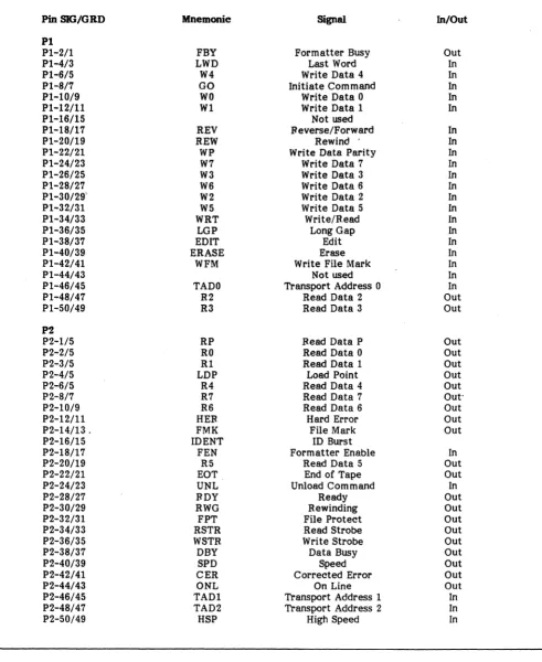
The following paragraphs describe the specifications and functions for each input signal required from the computer interface to the tape transport. Under the signal name are listed its mnemonic designation, the connector, active pin (and its associated ground pin) designations for its input signal line. Connector designations refer to the interface cable connector that mates with the corresponding card edge connector on the transport.
The pin numbers listed are for the two SO-pin "standard" ribbon cable connectors which will be provided with the unit. Table 1-3 summarizes the interface signals and pin numbers for the standard
connectors.·
-TRANSPORT ADDRESS
TADO, TAD1, TAD2 Level P1-46/4S
The status of these lines determines which of up to eight transports are selected by the controller. The transport address is set by means of a thumbwheel switch located on the Servo/Control PC board at the rear of the transport. The following list defines the tape transport addresses produced as a result of the various TADO, TADI, TAD2.
TADO TAD! TAD2 Address
0 0 0 SLTO
0 1 0 SLTI
1 0 0 SLT2
1 1 0 SLT3
0 0 1 SLT4
0 1 1 SLTS
1 0 I SLT6
1 1 1 SLT7
INITIATE COMMAND
GO Pulse PI-8/7
A pulse which initiates any command specified by the command lines described in the following paragraphs. Information on the command lines is copied in the corresponding formatter flip-nops on the trailing edge of the GO pulse. FBY is set true when the GO pulse is given with the selected transport ready.
COMMAND LINES
The levels on these lines issue a command to the formatter on the trailing edge of the GO pulse. The REV, WRT, WPM, HSP, ERASE, LGP and DEN levels must be held steady from O.S microsecond prior to the leading edge to O.S microsecond following the trailing edge of the GO pulse. See table 1-4 for Command Structure.
REVERSE-REV Level PI-18/17
A level which initiates reverse tape motion when true. When false, this level specifies forward tape motion.
1-9
WRITE
WRT Level
106-6809-009C
P1-34/33
Write mode is specified when this level is true; read mode is specified when this level is false.
WRITE FILE MARK
WFM Level PI-42/41
When this level and WRT are true, the transport will write a file mark on the tape.
ERASE
ERASE Level PI-40/39
Setting ERASE, WFM, WRT and EDIT true initiates a data security erase, erasing tape continuously from point of issue to about 1 meter beyond EOT. A fixed erase is issued by setting ERASE, WRT and WFM true, causing about 3.7S" of tape to be erased. A variable erase is initiated by setting ERASE and WBT true and is terminated by issuing LWD true. During variable erase the transport supplies Writes Strobes, to be used for distance measurement (each strobe is equivalent to 1 character space).
EDrr
EDIT Level P1-38/37
At present this line is used in conjunction with ERASE, WFM and WRT to initiate data security erase (see ERASE command).
mGHSPEED
HSP Level P2-S0/49
A level which causes the selected on line transport to operate in high speed mode.
REWIND
REW Pulse Pl-20/19
A pulse which causes the selected on line transport to rewind to load point. This pulse does not cause FBY to go true.
UNLOAD COMMAND
UNL Pulse P2-24/23
This pulse causes the selected transport to· go off line, rewind the tape, and when BOT is encountered, unload tape onto the supply reel.
LAST WORD
LWD Level P1-4/3
When this level is true during a write or erase command, it indicates that the next character to be strobed into the formatter is the last character of the record. LWD goes true when the last data character is placed on the interface lines.
FORMATTER ENABLE
FEN Level P2-18/17
LONG GAP
LOP Level PI-36/3S
A level which causes the selected (on line) transport to generate a 1.2" long IRG.
wam
DATA PABlTY AND WlUTE DATA UNDWP WO
WI W2
W3
W4
WS W6 W7
Levels PI-22/21
PI-I0/9 PI-12/l! PI-30/29 PI-26/2S PI-6/S PI-32/31 PI-28/27 PI-24/23
The 8 write data lines (9 in case of external parity option) are utilized to transmit write data from the controller to the formatter. WO corresponds to the most significant bit and W7 to the least significant bit of each character.
The first character of a record should be available on these lines per time defint!<1 in table 1-1 after DBY goes true and should remain until the trailing edge of the first WSTR is issued by the fQrmatter. The next :!haracter of information must then be placed on these lines within one-half a character period.
Subsequent characters of a record are processed in this manner until LWD is set true by the controller when the last character is transmitted.
1.6 INTERFACE OUTPUTS
(TRANSPORT TO CONTROLLER)
The signals listed below are supplied from the transport to the controller interface and include decoded read data, formatting status and transport status indications.
FORMATl'ER BUSY
FBY Level PI-21l
This level goes true on the trailing edge of the GO pulse when a command is issued by the controller. FBY goes false upon the completion of a block after Data Busy (DSY) goes false. In high speed mode FBY going true while DBY remains false indicates that the drive has entered a Reposition Cycle. Note that omitting Strap 11 on Servo/Control PC board ungates the GO pulse from FBY, allowing a command to be accepted with FBY true, provided that Data Busy DBY is false. This allows the next command to be accepted during the Repositioning Cycle.
DATA BUSY
DBY Level P2-38/37
This level goes true after the unit has ramped up to speed and the gap has been completed; DBY remains true until data transfer and the appropriate post record delay are completed.
CORRECTED ERROR
CER Pulse P2-42/41
When true, this pulse indicates that a single track dropout has been detected and the formatter is performing an error correction:
HARD ERROR
HER Pulse P2-12/l!
When true, this pulse indicates that an uncorrectable read error has occurred and that the record should either be reread or rewritten.
IDENTIPICATION
IDENT Level P2-16/15
When true, this level identifies PE tapes. PE tapes are detectable in the read forward mode by the presence of an identification burst on the parity channel.
PILE MARK
FMK Pulse P2-14/13
File mark is pulsed when a file mark is detected on the tape during a reati operation or during a write file mark operation. The FMK line will be pulsed after a complete file mark record has been read.
ON LINE
ONL Level P2-44/43
A level that is true when the on line flip-flop is set. When true, the transport is under remote control. When false, the transport is under local control.
READY
RDY Level P2-28/27
A level that is true when the tape transport is on tape; that is, when the initial load sequence is complete ·and the transport is not rewinding. When true, the transport is ready to receive a remote command.
PILE PROTECT
FPT Level P2-32/31
A level that is true when a reel of tape without a write-enable ring is mounted on the transport supply (or file) hub.
LOAD POINT
LDP Level P2-4/5
END OF TAPE
EDT Level P2-22/21
- -A level that is true when the EOT marker is detected in the forward direction. Goes false when the EOT marker is detected in reverse (REWIND).
REWINDING
RWD Level P2-30/29
A level that is true when the transport is engaged in a rewind operation or returning to the load point at the end of the rewind operation.
WRITE STROBE
WSTR Pulse P2-36/35
This line pulses each time a data character is written onto tape. WSTR samples the write data lines WP, WO-W7 from the controller and copies this information character by char~cter into the formatter write logic. The first character should be available prior to the first wri te strobe pulse and succeeding characters should be set up within half a character period after the trailing edge of each write strobe pulse.
READ STROBE
. RSTR Pulse P2-34/33
This line consists of a pulse for each character of read information to be transmitted to the controller. This signal should be used to sample the read data lines RDP, RDO-RD7.
COMMAND READ FORWARD *READ REVERSE
READ REVERSE EDIT WRITE
WRITE FILE MARK ERASE VARIABLE ERASE (FILE LENGTH) DATA SECURITY ERASE SPACE FORWARD (1 BLOCK) SPACE REVERSE (1 BLOCK) SEARCH FILE FORWARD SEARCH FILE REVERSE SEARCH FILE FORW ARD (IGNORE DATA)
SEARCH FILE REVERSE (IGNORE DATA)
REV H L L H H H H H H L H
L
H
L
READ DATA LINES
RP Levels
RO Rl R2 R3 R4 R5 R6 R7
106-6809-0110
P2-1/5 P2-2/5 P2-3/5 PI-48/47 PI-50/49 P2-6/5 P2-20/19 P2-10/9 P2-8/7
Each character read from tape is made available by parallel sampling the read lines with READ STROBE. Since the data- remains on the read data lines for a full character period, the corresponding RSTR pulses are timed to occur at approximately the center of the character period.
SPEED
SPD Level P2-40/39
A level which, when true, indicates that selected transport is in high speed streaming mode.
1.7 INTERFACE SUMMARY
Table 1-2 lists the states of the command lines required to implement the different transport functionS. Table 1-3 lists a sum mary of the 6809 standard two 50 pin connectors. The tatle includes the signal names, mnemonics and in/out designations. Figure 1-5 shows read-after-write timing relations for the normal start/stop mode.
WRT WFM ERASE EDIT
H H H H
H H H H
H H H L
L H H H
L L H H
L H L H
L L L H
L L L L
H H L H
H H L H
H L H H
H L H H
H L L H
H L L H
*Read Reverse applies to low speed mode only.
Table
1-2
Model
8809
Functional Command Structure
[image:13.612.326.562.66.171.2] [image:13.612.60.570.408.693.2]STOP RUN
TAPE VELOCITY
DATA ON TAPE
WRITE DATA STROBE
READ STROBE
PREAMBLE 1 POSTAMBLE
DATA BVTEllAST DATA BVTEj
1st
S=SPEED 1 PS T=TIME IN SECONDS TpD=PREAMB'LE DELAY • •
O~5
POSTAMBLE
TR=RAMP TIME=
.3~5
TRD=READ DELAY-
4i
TT=TOTAL WRITE DELAY • •
4~5
TWS=WRITE START DELAY=
.0~5
Figure 1-5.
Read Alter Write Timing
[image:14.612.62.561.71.712.2]106-6809-0130
Pin SIG/GRD Mnemonic Signal InIOut
PI
PI-2/1 FBY Formatter Busy Out
PI-4/3 LWD Last Word In
PI-6/5 W4 Write Data 4 In
PI-8/7 GO Initiate Command In
PI-IO/9 WO Write Data 0 In
PI-12/11 WI Write Data 1 In
PI-16/15 Not used
PI-18/17 REV Reverse/Forward In
PI-20/19 REW Rewind - In
PI-22/21 WP Write Data Parity In
PI-24/23 W7 Write Data 7 In
PI-26/25 W3 Write Data 3 In
PI-28/27 W6 Write Data 6 In
Pl-30/29' W2 Write Data 2 In
PI-32/31 W5 Write Data 5 In
PI-34/33 WRT Write/Read In
PI-36/35 LGP Long Gap In
PI-38/37 EDIT Edit In
PI-40/39 ERASE Erase In
PI-42/41 WFM Write File Mark In
PI-44/43 Not used In
PI-46/45 TADO Transport Address 0 In
PI-48/47 R2 Read Data 2 Out
PI-50/49 R3 Read Data 3 Out
P2
P2-1/5 RP Read Data P Out
P2-2/5 RO Read Data 0 Out
P2-3/5 RI Read Data 1 Out
P2-4/5 LOP Load Point Out
P2-6/5 R4 Read Data 4 Out
P2-8/7 R7 Read Data 7
Out-P2-10/9 R6 Read Data 6 Out
P2-l2/11 HER Hard Error Out
P2-14/13 _ FMK File Mark Out
P2-16/15 IDENT ID Burst
P2-18/17 FEN Formatter Enable In
P2-20/19 R5 Read Data 5 Out
P2-22/21 EOT End of Tape Out
P2-24/23 UNL Unload Command In
P2-28/27 ROY Ready Out
P2-30/29 RWG Rewinding Out
P2-32/31 EPT File Protect Out
P2-34/33 RSTR Read Strobe Out
P2-36/35 WSTR Write Strobe Out
P2-38/37 DBY Data Busy Out
P2-40/39 SPD Speed Out
P2-42/41 CER Corrected Error Out
P2-44/43 ONL On Line Out
P2-46/45 TADI Transport Address 1 In
P2-48/47 TAD2 Transport Address 2 In
P2-50/49 HSP High Speed In
Table 1-3
Model 6809 Interface Summary
[image:15.613.60.551.92.692.2]-.-
...
"......
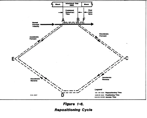
-~FIgure 1-6.
ReposItIonIng
Cycle
1.8 STREAMING MODE
TIMING CONSIDERATIONS
When in the streaming mode the Model 6809 requires approximately 300 msec to ramp to speed from a stopped state, moving about 15 inches of tape in the ' process. The prolonged ramp necessitates a repositioning cycle each time a command is not received during ~he allotted 4.0 msec period in the interrecord gap, called the Command Reinstruct Time. The Command Reinstruct Time and the repositioning cycle are illustrated in figure 1-6. The Command Reinstruct period starts when Formatter Busy (FBUS) goes false at the end of a block, shown as point A in the figure, and ends 4.0 msec later, when FBUS goes true again (point B). Note that the 4.0 msec Command Reinstruct Time can be extended to 10.0 msec by using the long gap mode. If a command is received between points A and B (GO pulse issued) the transport will acknowledge it by setting Formatter Busy (FBY) true and will continue streaming, provided the command is the same as the previous command. If no new command is received by point B, the transport will automatically reposition by first decelerating to a stop (point C on figure 1-6),
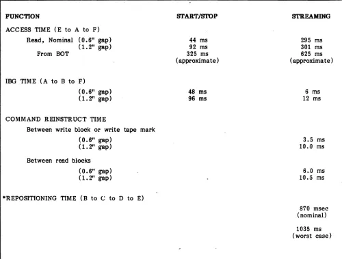
accelerating backwards and passing over the interreCOl"d gap 0, then ramping down to a stop at E. At this point FBUS goes false and the transport waits for a command to be issued. When the next command is issued, the transport accelerates from point E to attain normal velocity and executes the command. The time between the stopped state (E) and the transfer of the first data byte (F) is defined as the Access Time. Access Times for both the streaming and start/stop modes are listed in table 1-5. The table also lists the interrecord gap times, the Command Reinstruct Time, and the Repositioning Time, defined as the time between the end of the Command Reinstruct Time (B) and the stopped state (E).
FUNCTION
ACCESS TIME (E to A to F)
Read, Nominal (0.6" gap) (1.2" gap) From BOT
IBG TIME (A to B to F)
(0.6" gap) (1. 2" gap)
COMMAND REINSTRUCT TIME
Between write block or write tape mark
(0.6" gap) (1. 2" gap)
Between read blocks
(0.6" gap) (1.2" gap)
*REPOSITIONING TIME (B to C to D to E)
START/STOP
44 ms 92 ms 325 ms (approxima te )
48 ms 96 ms
108-8809-015B
STREAMING
295 ms 301 ms 625 ms (approximate)
6 ms 12 ms
3.5 ms 10.0 ms
6.0 ms 10.5 ms
870 msec (nominal)
1035 ms (worst case)
*Repositioning time for error recovery is somewhat greater depending on length of record being read in reverse.
Table 1-6.
Streaming and Start/Stop Timing Specifications
..
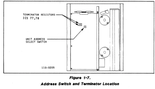
[image:17.612.56.556.73.452.2]TERMINATOR RESISTORS
Ies 77 .18
UNIT ADDRESS
SELECT swnCH
110-0205
o
o
'I
[image:18.612.54.572.64.362.2] [image:18.612.56.573.560.726.2]1
Figure
1-7.
Addre •• Switch and Terminator Location
1.9 TRANSPORT DAISYCHAIN CONNECTION
Up to 8 transports may be connected in a daisychain configuration. To connect the transports. in this fashion 2 daisychain cables, Kennedy Part Number 190-6999-xxx should be ordered. The first digit of the dash number indicates the number of transports to be connected by the cable. The last two digits of the dash number indicate the total length of the cable in feet. Thus cable part number 190-6999-420 would specify a 4 transport daisychain cable, 20 feet long with 4 feet between each transport and 4 feet between the first transport in the chain and the controller. The first connector on the cable, to be plugged to the controller, is a 50 pin connector Kennedy Part Number 121-0166-001. The connectors
CONTROLLER
1
.n
..12110-0206
STREAMER
ttto
to be plugged to the transports are 50 pin connectors Kennedy Part Number 121-0162-002.
When a daisychain connection is used it is necessary to assign each transport with a different address number using the address selection switch located on the Servo/Control PC board at the rear of the unit, as shown in figure 1-7. The address assigned to the transport should be between 0 and 7. Single transports should always be assigned address O. In addition the terminator resistors, located on ICs 77 . and
1S
on the Servo/Control board, as shown in. figure 1-7, should be removed from all but the last transport in the daisychain. A daisychain configuration is shown in figure I-S. Note that if the total cable length exceeds 20 feet, active repeaters must be used.r--DAIS'«:HAIN CABLE
/ , ICENNEDY PH 190-e999-XXX
---I.
-.1
- - ]
..II ..12 ..I • ..12 UP TO.,...
STREAMER .... ' STREAMER TERMINATED 7
Figure
1-8.
206-6809-001B
SECTION II
INSTALLATION AND OPERATION
2.1 INSTALLATION
2.1.1 INSPECTION
Prior to installation, inspect thoroughly for foreign material that may have become lodged in the reel hubs and other moving parts.
2.1.2 MOUNTING
Physical dimensions and outline of the tape transport are shown in figure 1-1. The transport requires 22.7 inches vertical mounting space on the standard 19 inch rack. Transports in a system configuration should be arranged to require less than 20 feet of cabling between the tape controller and the furthest tape unit.
2.1.3 SERVICE ACCESS
Access to the transport electronics is available from the rear and sides of the unit when the unit is extended on its slides. To gain access to the PE Read and the Read Amplifier PC boards first remove the interconnect board, then the Servo/Control PC board retaining screws and standoffs, and swing the Servo/Control PC board open on its hinge. The PE Read is the top of the two exposed boards, the Read Amplifier is the lower of the two. Access to the Tape Tension PC board is gained by removing .the PE Read and the Read Amplifier retaining nuts, and swinging the boards open, exposing the tape sensor assembly. The Voltage Regulator PC board is located between the two reel motors. The Power Amplifier PC board is attached to the heatsink assembly, to the left of the unit (when facing the unit from the rear). For servicing electronics test points are provided by standoff pins on the circuit boards, and are identified by upper case letters near each test point.
2.1.4 INTERCABLING
Installation of the unit requires two 50 line ribbon cables and connectors, matching the two edge connectors on the Interconnect PC board. Connector pin assignments are listed in table 1-3.
2.1.5 POWER CONNECTIONS
CAUTION
Before connecting the unit to the power source, make certain the line voltage is the correct voltage (115 or 230 vac) and that the proper fuse has been installed.
A power line module, including the power connector, voltage selector and the fuse, is accessible from the
top of the unit. Voltage selection is accomplished by the insertion of the selector PC board in such a manner as to show the selected voltage designation through the plastic window. Note that the fuse must be removed prior to changing the voltage selection, and the properly rated fuse for the new voltage must then be installed.
A detachable power cord is supplied with the tape unit. The power cord is 9 feet long and has a NEMA three-prong (two power, one chassis ground) plug for connection to the power source.
2.2 OPERATION
2.2.1 INTERFACE
Before placing the unit in operation, make certain that the interface connection procedures outlined in Section I have been performed.
2.2.2 CONTROLS AND INDICATORS
Figure 1-2 lists the controls and indicators for the tape transport and describes the functions of each. The test panel controls are described in paragraph 4.7.
2.2.3 PRELIMINARY:ElROCEDURES
Before placing the unit in operation, proceed as follows:
a. Check the tape transport read/write head, erase head, capstan and idlers for any foreign
material.
b. Check for correct line voltage and make sure that correct fuses are installed (paragraph 2.1.5).
c. Push primary power switch on.
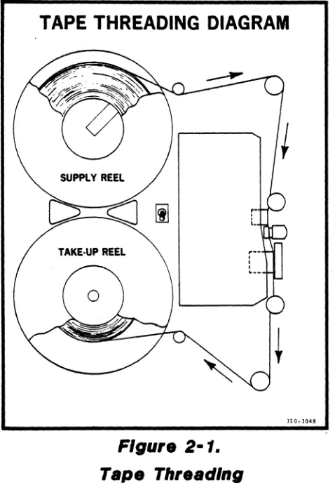
2.2.4 TAPE THREADING
To thread the tape on the transport, proceed as follows:
2-1 .
a. Raise the latch of the quick-release hub and place the tape file reel to be used on the supply hub (figure 2-1) with the write-enable ring side next to the transport deck.
b. Hold the reel flush against the hub flange and secure it by pressing hub latch down.
d. Holding the end of the tape with a finger, wrap a tew turns clockwise around the takeup reel
hub.
2.2.5 TAPE LOADING
Pressing and holding the LOAD pushbutton for approximately 0.5 second energizes the reel servos and initiates a load sequence. Tape advances to the load point marker and stops.
If tor some reason the load point marker is already past the sensor as, for example, in restoring power after a shutdown, tape continues to move tor approximately 6 seconds and then automatically initiates rewind.
Once pressed, the LOAD switch is inactive until power has been turned otf or tape is removed from the machine.
2.2.6 PLACING TAPE UNIT ON UNE
After the tape is properly threaded and has been loaded and brought to the load point, press the ON LINE pushbutton and check that ON LINE indicator illuminates. (The REWIND pushbutton is disabled when the tape unit is on line.) On line status enables the tape unit to be remotely selected and to perform all normal operations under remote control.
TAPE THREADING DIAGRAM
llO~ )048
Figure 2-1.
Tape Threading
2.2.7 TAPE UNLOADING AND REWIND
Provision is made in the 6000 series transports for rewinding a tape to the load point under remote control. However, this operation may also be performed manually. Proceed as follows.
a. If the ON LINE indicator is illuminated, press the ON LINE pushbutton. Check that the indicator extinguishes when pressure is removed.
b. Press the REWIND PUShbutton. The tape will now rewind to the load point marker.
c. After the tape has been positioned at the load point under remote or local control, press the REWIND pUShbutton to unload the tape past the load point to the physical beginning ot the tape.
NOTE
The rewind sequence cannot be stopped until the tape has rewound either to the load point or until tape is rewound onto the supply reel after an unload sequence.
2.2.8 POWER SHUTDOWN
A tape transport should not be turned oft when tape is loaded and is past the load point marker. Kennedy transports are designed to prevent physical damage to the tape in the event of power failure, and to minimize operator error which could destroy recorded data. In the event of power failure during tape unit operation, manually wind the tape forward several feet before restoring power. When power has been restored, press the LOAD pushbutton. If load point is not reached within 6 seconds the tape will rewind, searching for load point. If desired, the tape can then be advanced to the data block nearest the point at which the power failure occurred, by initiating the appropriate control commands.
[image:20.612.72.311.374.723.2]306-6809-001B
SECTION III
THEORY OF OPERATION
3.1
INTRODUCTIONThe Model 6809 is a microprocessor controlled tape drive that produces formatted phase encoded data. The microprocessor plays an important part in all aspects of transport operations, from command interpretation to reel motor control. The overall flow chart of the microprocessor program is shown in figure 3-1. Type 8039 microprocessor and its associated 4-K ROM are located on an Emulator board which produces the equivalent interconnection to the 8049 chip and plugs into the Servo/Control board. The Servo/Control board, the large board at the rear of the unit, includes the microprocessor network, the command interface, the entire write electronics and additional functions. Outputs from the Servo/Control board are supplied directly to the controller interface through the Interconnect board, and to the power amp, which provides the power inputs to the reel motors. Located below the Servo/Control board are two connected boards. The lower of the two is the Read Amplifier, containing the analog circuitry which amplifies the signals from the read head. The upper of the two boards is the PE Read, which processes the analog data, converts it to logic levels, performs error correction and supplies the decoded data to the controller. Additional electronic modules of the 6809 include the Voltage Regwator, the Tape Tension Sensor, the Control Panel and the Reel Sensor boards.
3.2
SERVO/CONTROL BOARD3.2.1 INTRODUCTION
The Servo/Control board performs all control functions associated with the tape transport operation. Included on the board are the microprocessor network, which decodes the controller commands and initiates the required transport motions, and the PE data generation circuitry. Listed below are the functions performed by the board and the schematic page on which they appear.
Servo/Control
Page Number Functions Performed
1 Front panel control Power failure detection Tape motion counter File protect circuitry Write/erase current drivers
2 Reel size sensor circuitry Data I/O
Microprocessor network Bus addressing
Takeup servo circuitry and DACO
3-1
Servo/Control
Page Number FtDlctions Performed
3
4
5
6
BOT/EOT, on line interrupt generator
Takeup and supply reel DACS Crystal clock and dividing network Tension sensor circuitry
Supply servo control
Interrupt and I/O control Inputs from controller Outputs to controller Address selection circuitry Command decoding
Write data inputs Phase encoding circuits Formatting circuits Write head drivers
Tape motion detection Tape direction detection Repositioning counter Velocity counter
3.2.2 MICROPROCeSSOR INPUT/OUTPUT
Inputs and outputs to the microprocessor are supplied on two 8-bit wide ports, PI and P2, and an 8-bit data bus. The ports are quasi-bidirectional while the bus is truly bidirectional. The bus is used for transmission of both external address and data. As an example assume that the microprocessor is given an instruction to monitor the transport control panel status lines, which are presented to bus buffer IC56 (page 2-A2, type 5426). In this case the address of ICS6 (buffer 7) is presented on the data bus, is passed through bidirectional buffer IC85 (since READ/ is false), and is latched into IC47 on the trailing edge of Address Latch Enable ALE. The outputs of IC47 are decoded by IC31, a 3 to 8 decoder whose outputs are gated with the READ/ signal output by the microprocessor. READ7/ true at IC14-11 is used to enable buffer IC56, providing the control panel status information to the data bus, back to the microprocessor through IC8S, which now operates in the read mode with data flowing toward the 8049 - chip.
3.2.3 POWER UP SEQUENCE
[image:21.612.315.542.144.395.2]310-3034
Figure 3-1.
NOTE I
NOTES:
I I
I
I I I
I
I
I I
I
I I
I
I
I
I I I
I
I
I
... Ulll_'.
,...---,
I
I
I
I
I
IIOTE Z I
I I I I
IOTE 3 I
I t
I
I I
I I I
I 'rES I
1..---...1
1. PRESUN' MASTlR RESET ON COITROL PAIlL INITIALIZES MICROPIOCESSOR.
Z. POI'U UP/LOAO SEQUENCE IIITIALIZU TAP! LEN'TN RIiISTUI, WAITS FOR TAlEUP; SU»U REU MOYOIS TO STO'.
3. THIS LaO' COIII'ENSATES FOI OVERSHOOTlN' LP IN HIIN S'UD REYERSE MODE.
4. STATUS REQUEST liT ON UNE 07 GOES LOW FALSE ON TRAIUN. EDIE OF GO/PULSE FROII CO.TlILLE~.
5. TAPE LENITH IS MEASURED IT COUNTlN' 'OST PULSES FRail CAPSTAN CIRCUIT.
&. TA,E REPOSITION SEQUEl": TAPE ~ OATA ILK
I'm;:i
dCll
... I. .. ~~1.
"::rto
L ~':-tl~~~~a"""" 'O~~~:.f't
DICt... ,~\
Iftvt.'"t.-;,;- - - - --~t\\.\ .. -:.t.
~$t " .. I.~
_ _ _ _ _ _ _ _ _ _ _ POSITIOwr., TIllE - - - REPOSlTlONIN' TIME
(A"ROI. 30 IN. TAPE IEWOUNO) 7. liT 07 IS A STATUS REQUEST liT AT TMIS .. OINT II 'R06IAN.
[image:22.612.70.573.47.702.2]prior to the start of program execution. When PRESET/ goes false the MPU will test its Tl input (Tl low indicates stable power). If power is not stable the microprocessor jumps to a subroutine which performs an orderly power down sequence. Note that switch S2, located on the board, can also be used to issue a M RESET/in case of an abnormal condition that arises while testing the unit. Warning of an imminent power failure is provided by the POWER DROPOUT signal, supplied by the Voltage Regulator board. The processor will then check for power stability and take appropriate action.
Crystal Oscillator and Divider Network (Schematic Type 5426, page 3 of 6)
The master clock frequency of 10.24 MHz is supplied by a crystal oscillator consisting of IC6 and its associated circuitry. The master frequency is
supplied to the microprocessor as XTLI. Additionally, it is divided by counters IC4, IC11, ICI2, and IC13 to provide the other frequencies required by the unit. CLKl, used to clock the tape position counter, is 853 KC in high speed, 106.6 KC in low speed, and 2.0 KC during the ramp. Frequency 2F, used by the data encoding and decoding sections,
is 320 KC during high speed operation and 40 KC during low speed operation.
3.2.4 MICROPROCESSOR SERVO CONTROL
The microprocessor receives reel size data, tape position data and tape speed data from the transport, synthesizes those and compares the derived information with a table stored in memory. It then outputs the required current information to the reel servos through a set of D to A converters.
The reel size is determined by a pair of LED/ photosensors located under the supply reel which detect reflections from the reel surface, determining whether a 10.5", an 8.5" or a 7" reel is mounted. The reel size plays an important function in determining the inertia factors.
The tape speed is determined by an optical tach rotated by the takeup tape roiler. The optical 'tach output is picked up by two detectors, one of which is
adjustable so that the signals at test points 11 and 12 are square waves that are 90 degrees out of phase with respect to each other. Direction of motion is
determined by which of the two signals leads the other as shown by the output of flip-flop IC112-9 (low in forward direction). The tach outputs are digitized by a circuit consisting of ICs 113, 118, 87, 112 and 103 (page 6 of 6, type 5426 schematic). The stop bit
is generated by a circuit consisting of a differentiator, a rectifier and an adder. The sinwt and coswt waveforms output by the optical encoder are differentiated by the input capacitors and two sections of ICI04, producing a waveform proportional in amplitude to the angular frequency, and hence to tape velocity. The output of the differentiator stages are then rectified by the four sections of IC125, are added and supplied to an integrator stage which
3-3
306-6809-003B
produces a DC level proportional to the tape velocity. The velocity profile can be monitored at Test Point 7. When the velocity profile approaches zero the circuit generates STOPPED/ true.
The circuit consisting of ICs 102, 124 and 100 forms the POST pulse on the leading edge of the POST square wave. Elapsed time between POST pulses is counted by the counter consisting of ICs 32 and 48. Upon the arrival of each POST signal the counters output is latched into IC49 and the counters are cleared. The POST pulse also sets flip-flop IC30, informing the CPU at PI-6 that the speed counter is ready to be read by the processor. The CPU then supplies READ6/ true to monitor the count, resetting IC30 and IC49.
A repositioning counter is used to identify the precise starting point of a high speed repositioning cycle. The counter consists of three 4-bit up/down counters in succession, ICs 121, 122 and 123 (see 5426 schematic, page 6-83). The repositioning counter is clocked by POSTS and counts UP when the tape is moving forward and DOWN when the tape is moving in reverse. Recall that the repositioning cycle starts when a command is not received during the command reinstruct time at the end of a block. Whenever Data Detect goes low at the end of the block the output of IC97-11 goes low, setting IC32-6 low. The pulse generating network consisting of ICs 102-12, 1.02-15, 124 and 10.0 supplies a loading pulse one CLK1 wide to load the repositioning counter with all Os. If repositioning is initiated during an erased segment of tape the loading pulse is generated by Data Busy DBY going false and that point would be identified as the starting point of the repositioning cycle. Once a repositioning cycle is started the tape ramps down to a stop while the counter is counting UP the number of elapsed POSTS. The tape then reverses direction and ramps backwards as the counter counts DOWN. When the counter returns to aliOs it outputs ZERO high to the microcomputer, indicating it has reached the starting point of the repositioning cycle.
The POST pulse is also used to clock the tape length counter. The counter is a 21 bit counter, whose least significant 5 bits consist of IC68 and IC54 (5426 schematic, page I-D1). The remaining 16 bits of the up/down counter are internal to the processor. Each POST count is equivalent to 3/160 inches of tape, or 0.48 mm. The length counter is reset at load point or when the processor supplies DISABLE/ true, disabling the servos.
extra constant, provided by the processor, to ensure proper acceleration.
Tape tension information is supplied by the Position sensor Type 5764 board, located beneath the PE Read. The position sensing circuit consists of an oscillator, including comparator ICl, whose frequency varies according to the position of the tension arm, which in turn varies the effective capacitance of the dashpot. The oscillator output is divided by decade counter IC2 and supplied to integrator IC3. The integrator output is averaged by the network consisting of R4, R5 and CS. The DC average is summed with an offset provided by R15, R17, is amplified and output to the Servo/Control board. Potentiometer R9 is adjusted to provide Ov output
w~en the tension arm is centered in its arc. 3.2.5 INTERRUPTS
The MPU will be interrupted from its normal program now whenever, a loadpoint or end-of-tape marker is encountered. The Interrupt (INT /) is generated by circuitry that includes ICs 81, 92, 82, 45 and 69 (5426 schematic, page 3-A). If both LP and EOT indicators are activated, it signals broken tape and the MPU disables the servos and sets both reel motor brakes.
An interrupt is also generated whenever the ONLINE pushbutton is pressed while tha tape unit is selected and tape is loaded. In that case the MPU will output the transport status to the tape controller via buffer IC36 (page 4-C4). Pressing the control panel RESET pushbutton also causes an interrupt, stopping tape motion in the Test Mode and allowing a changing of test function.
3.2.6 CONTROLLER INTERFACE
When the tape unit is addressed, on line and selected, IC3S (page 4-C3) is constantly scanned by the MPU, looking for a command from the tape controller. New commands are latched into ICs 73 and 75 by the GO pulse, and are encoded by ROM IC74 (page 4:-D3). The encoded commands are placed on the MPU bus by buffer IC3S. FBUSY and RWDG are latched by the incoming control command and are subsequently reset by software control.
3.2.7 PHASE ENCODED DATA GENERATION
The 5426 board also includes the entire PE data generation circuitry. Write data in the form of logic levels, supplied from the controller interface, is converted into phase encoded data by the PE write circuits, using the crystal generated 2F frequency. The PE formatting circuits generate the writing of the preamble and postamble, and the ID burst on channel P.
During power up, IC93, IC52 and IC44 are pulsed low by MRESET /. This ensures that the syncronous logic in the write circuitry is properly initialized. Signal 2F is twice the write frequency: 40 kHz at 12.5 ips and 320 kHz at 100 ips. The write frequency is available at IC67 pin 8.
Upon reception of a write command the MPU will set DATA and WRITE ENABLE true; thereby putting a low on the 5/ input of IC26 pins 2 and 3. The Q
output of IC26 will then go high, enabling counters IC94 and IC9S to count up to 40 beginning with the next available clock pulse. At the same time the clear inputs of IC50 and IC52 will go high allowing the transfer of 40 0 characters per channel to the write head drivers.
On the count of 40, IC9S pin 12 will be true, thereby resetting IC26 pin 9. With the arrival of the next clock pulse IClO pin 8 will go high, thus writing a 1 character on all channels.
The next clock pulse will force ICI0 pin 8 low and IC92 pin 8 high. This allows transfer of data from the controller to the PE write electronics by means of the write strobe generated by IC43, IC2 and IC3. Write parity can be internal or external; this is made possible by IC8 and jumper straps 7 and 8.
When the controller has written the desired amount of data it will issue a signal (LWD/) along with the last byte of data. The write control will then inhibit any further transfer of data by setting the clear inputs of IC40 and IC43 low. A 1 character is then written followed by 40 Os; at which point QD of IC98 will go true and place a low on IC26 pin 4. This results in loading the counters with zero and Q output of IC52 will go false on the next clock pulse, thereby clearing IC50 and IC52 pin 5. This completes the write cycle and the tape unit is now ready for the next command from the controller.
Jurnper straps 1 through 6 are provided so that the user may choose which of the three optional channels will be written on during a filemark.
ID burst is written on channel P only. This is performed by IC42, IC25 and IC52.
The network consisting of nip-nop ICs 67. 2 and 43 is used to generate the two write clocks. One clock is used to strobe the write data into the write buffer consisting of ICs 23 and 40. The other is supplied to the controller as Write Strobe WSTR to synchronize the write data transfer to the transport.
3.3 READ AMPLIFICATION STAGES
The read signal output by the head is in the order of 2 to 3 millivolts. It is·amplified by a preamplifier stage located on a mini PC board soldered directly to the head, eliminating any noise problems caused by wire leads. The preamp stage amplifies the read signal by a factor of 10 to 15, and the amplified signal is supplied to Read Amplifier type 6470, the lower of the two boards located below the Servo/Control board.
The Read Amplifier. board amplifies the signal, peak detects, digitizes it and provides the Data Detect output. The Read Amplifier consists of nine identical channels; consequently only channel 3 will be described (see Read Amplifier type 6470, sheet 1 of 3). The signal from the preamplifier is supplied to an amplifier stage, IC38, whose output at test point 3 is adjusted by potentiometer R6 to 4v peak to peak. FET switch Ql is used to adjust the gain for high and low speeds. At high speed the output of comparator IC2'3 swings to +15v, turning Ql on and reducing the output gain to compensate for the higher head output. The amplifier output is differentiated by the network consisting of C8 and R11 (also R12 in high speed) and supplied to zero crossover detector ICI2, providing
pea~ detection for the input signal. The output of the crossover detector is filtered by Schmitt trigger ICA and associated components, and is output to the PE Read board through connector Jl, provided that Channel 3 Data Detect is true. Data Detect is generated by supplying the amplifier stage output to a pair of IC27 comparators. One input of each comparator is tied to a clipping level, normally 1096 of the signal level. Th~ clipping levels prevent base line noise from being interpreted as data, generating Data Detect true only when the signal exceeds the clipping levels.
3.4 PHASE ENCODED DATA RECOVERY
3.4.1 INTRODUCTION
The phase encoded data is located on PE Read type 5326. Phase encoded data is read using a single phase locking oscillator, nine parallel read channels, and a read envelope detection network. The phase locking oscillator tracks one of the data channels and provides the nine read channels with the clock used to synchronize data decoding. The read channels, in addition to decoding the data, deskew the data, detect single track errors and perform single track error correction. The data envelope network monitors the number of valid channels, inhibiting data recovery unless eight of the nine channels contain valid data. These functions are described in the following paragraphs.
3.4.2 PHASELOCK LOOP
THE CONCEPT
The phase lock loop generates the DATACLK, a clock at 32 times the input data rate, used to synchronize
3-5
306-6809-005B
the data recovery functions. This frequency is derived using a voltage controlled oscillator whose center frequency is 32 times the data rate. The oscillator output is divided by 32 and its phase is compared with the phase of a reference data channel (channel 2 or channel P) during the data and a crystal derived frequency during the gaps. The output of the phase comparator is supplied to an integrating operational amplifier that supplies a corrective voltage to the input of the VCO. If the reference channel and the VCO output are in phase, no change in the corrective voltage will occur at the VCO input.
If the VCO output lags the input reference channel, the op amp will provide increased output voltage which will increase the ~rrective voltage to the VCO until the phase lag is corrected. Similarly, if the VCO output leads the input data, the operational amplifier will reduce the corrective voltage input to the VCO until the oscillator slows down enough to match the input reference phase.
THE DETAILS
(Reference 5326 schematic, sheet 4 of 6)
Voltage Controlled Oscillator and Dividing Network
The main component of the tracking oscillator is the voltage controlled multivibrator IC3. The multi-vibrator center frequency is selected by capacitor C8 to be 32 times the high speed data rate. The output of IC3 is routed through ECL-TTL conversion network including Q2, and through IC10 NOR gate. In high speed HIILO/ high passes the VCO output through ICI09-5 and ICI09-8 to become the DATACLK at 32 times the high speed data rate. In low speed the VCO output is divided by 8 through ICI08 and is gated through IC109-3 by LOIHII high to become DATACLK at 32 times the low speed data rate. DATACLK is supplied to a dividing network consisting of D flip-flop IC14 and 4 bit counter IC7 in tandem. The frequency is divided by 2 to supply SCLK (16 x data), divided by 8 to supply RCLK (4 x data) and divided by 32 to supply the data rate frequency as one input to the phase comparator· at IC9-H.
Reference Frequency Selector
The reference input of the phase comparator accepts one of three reference frequencies, 2F/2, DETP/, or'· DET2/, depending on the status of the DATA DET and SLT2/lines. During the interrecord gap Data Detect DAT ADET, supplied from the control board at pin
JI-ll, is low, setting the B input of 4 to 1 multiplexed IC80 lOW, supplying the 2F frequency divided by 2 to the phase comparator.
selecting channel 2 as the reference channel to the phase comparator. SLT2/ will go high omy if channel 2 has been dropped and channel P is valid, in which case SLT2/ high will select channel P as the reference channel input to the phase comparator.
The Phase Comparator
The phase comparator consists of 2 D nip-flops on IC9, and associated gating. The reference frequency, usually DET2/ during the data block, is supplied to the clock input of the upper ICg flip-flop. The output of the YCO is divided by 32 and supplied to the clock input of the lower IC9 nip-flop. If the YCO output frequency and the reference channel are in phase, both flip-flops are toggled to the set state simultaneously and are immediately reset following a propagation delay by NAND gate IC8-S.
When both flip-flops are reset, the Q output of the upper flip-flop sets the output of NAND gate IC8-3 high, the Q output of the lower flip-flop sets the output of IC8-8 low. Consequently the voltage divider network including resistors R3, R5, R6 and R4 provides about S volts at the summing point of the operational amplifier IC2. The noninverting input is supplied with 6.1 volts by the dividing network including R7, Rll and R12. In this case the output of
the op amp supplies minimum current to summing transistor Ql and no correction voltage change occurs across load resistors R14 and Rll.
When the phase of the YCO output leads that of the reference channel, the lower IC9 flip-flop is set first, causing the output of nand gate Ica to swing high for the duration of the phase delay, supplying 12 volts across the resistors at the inverting input of the op amp. This increases the positive feedback current of the op amp and reduces the output current to summing transistor Q1. As a result, the corrective voltage of the YCO is reduced until the output frequency slows down sufficiently for the phases to match. When the YCO output lags the reference channel, the upper D nip-flop will be set first and the output of NAND gates IC8-3, ICa-8 will be grounded for the duration of the phase delay. This will produce a negative feedback current, increasing the positive output current to summing transistor Q1. As a result the corrective voltage to the VCO will be increased until the YCO frequency speeds up sufficiently for the phases to match.
3.4.3 DROPOUT RESYNCHRONIZATION
THE CONCEPT
Either channel P or channel 2 are used as the reference channels for the tracking oscillator. Should a dropout occur in the reference channel, tracking is automatically switched to the alternate channel. Since a phase difference may exist between the tracking channel and its alternate due to skew, there may be a gap during the switching which could be interpreted by the phase comparator as a drastic slow down or speed up of data, and synchronization could
be lost during the attempted correction. This. condition is averted by a detection network t~!
preloads the data counter during the switchover
in
reference channels, maintaining synchronization of tracking.THE DETAILS
(reference schematic 5326, sheet 4 of 6)
DROP P and DROP 2 are connected to a flip-flop consisting of two segments of IC37. Normally, when both channels are read properly, the flip-flop output at IC37-10 would be low, generating SLT2/ true. SLT2/, supplied to multiplexer IC18, causes channel 2 data to be input to the tracking oscillator network. When a dropout occurs on channel 2, DROP 2 high clears flip-flop IC37 generating SLT2/ high. For one DATACLK period the inputs to exclusive OR gate IC11 would be ~pposite in polarity, generating a positive pulse. This pUlse, indicating a switch over in tracking channels, clocks J-K flip-flop ICI9 to the set state. The Q/ output of the flip-flop preloads the tracking oscillator dividing network (IC7, ICI4) to maximum count minus one. The switchover pulse output by IC17-11 is also gated through IC5-8,
ICl09-11 (provided LOCK/ is false) and clears the phase-comparator flip-flops IC9, preventing excessive correction voltage from drastically altering the tracking osciL.ator frequency.
3.4.4 DATA DECODING, DESKEWING AND SINGLE TRACK ERROR DETECTION
Read data from the transport read amplifiers is supplied to nine parallel decoding channels, each consisting of a latch, a ROM, and a state counter. Using the counter outputs, the ROM distinguishes between data transitions and interphase transitions, and determines whether the data transitions occur within the required time frame. The ROM supplies three latched outputs: Shift In <SI), Error in Channel (EIN), and Transition Detect (TDET). SI is used to shift the data and ElN into the deskew register. EIN is also supplied to plurality check circuitry used to generate the data envelope. TDET is used to reset the state counter after each data transition.
This is accomplished by delaying the Shift Out pulse of a channel that contains a 1 bit at the deskew register output until all channels contain a 1 bit at their outputs. At this time Shift Out is generated to shift the deskewed data of all nine channels to eight bit delay registers, used for postamble recognition. After eight clock periods the data is output to the interface, accompanied by a Read Data Strobe.
THE DETAILS
(schematic 5326 sheet 6 of 6)
Read Decoding and Error Detection
Since the nine decoding and deskewing networks are practically identical, only channel P will be described in detail. It will remain to the reader to translate IC reference numbers to the particular channel examined.
The PE decoding network consists of a hex D flip-flop latch (IC28), a ROM (lC29) and a six bit counter (lC30, IC3l). Channel P read data is supplied from the read amplifiers at pin Jl-12, is inverted (twice in read reverse mode) and is supplied to one latch input. One DATACLK pulse later (DATACLK is 32 x data rate) the read data is supplied to a ROM address input and is supplied to another latch input. The second latch supplies the data to another ROM address following a 1 DATACLK delay. The outputs of the two latches will be in the same state when no transition has occurred, and will be in the opposite state for 1 DATACLK period following each transition. The counter, also clocked by DATACLK, supplies the ROM with the count reference necessary to idenUfy the time of occurrence of each data transition. This is accomplished by dividing each character frame into six states. Five states are a quarter of a character frame wide, and the sixth is one DATACLK period wide. When a transition occurs, the ROM identifies the transition as either valid data, an interphase transition, or an error transition, according to the time of its occur.rence. Interphase transitions occur in states 2 and 3,
between 25% or 75% of the character frame. Error transitions are defined as transitions 'occurring too early (during state one, within 25% of a character frame since the last data transition), . or too late (when no transition has occurred withi